PCB assembly overview

The complete PCB generally contains two parts, One is the production of bare PCB boards, and the other is the assembly and packaging of electronic components. After the bare circuit board is made, it is the assembly and packaging of the PCB.

directory

What is PCB Assembly?

We have talked about how PCBs are made through PCB mechanics which include several processing steps. However, further processing is required before the circuit board can be used, that is, assembly PCB. The bare board will be made with fiberglass, copper lines and other metal parts, held together with epoxy resin and insulated with a solder mask. The solder mask turns the bottom surface into green.

After a PCB is prepared, electronic components and parts can be assembled on it. And some electronic components are going to be mounted on the PCB. Then this board is called PCBA and can be used for electronic products. Therefore, PCB Assembly refers to the manufacturing procedure of connecting electronic components to the printed circuit boards by using soldering, PCBA for short. The upgrade of electronic products has led to an increasing demand for PCB assembly prototypes.
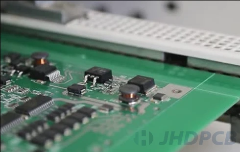
PCB-assembly-overview

How to Assemble PCB?

PCB assembly process consist of adding solder paste to the board, picking and placing components, soldering, inspection and testing. The whole assembly process need to be monitored to ensure highest quality of the products are produced. (PCB prototype assemblies are early samples of products built with the sole purpose of testing design ideas to see if they work)

What Are the PCB Assembly Process?

The PCB assembly process is not complex, including several automatic and manual steps. The PCBA process always starts out with the most basic unit of the PCB:

Use mechanical fixture to place a thin stainless steel template on the plate. The solder paste should be spread evenly on the exact locations needed of the circuit board.
Solder paste ingredients: The solder paste itself is a gray substance composed of tiny metal balls, also known as solder. These tiny metal balls are made up of 96.5% tin, 3% silver and 0.5% copper. Solder paste mixes solder with flux. (Flux:A chemical designed to help solder melt and bond to surfaces) Solder paste, a gray paste, must be applied to in the right amount the board in the correct place.

In a professional PCBA production line, mechanical grippers hold the PCB and soldering template in place. The applicator then places the solder paste in the exact amount on the desired area. The machine then applies the slurry to the template, spreading it evenly over each open area. After the template is removed, the solder paste remains in the intended position.

After applying the solder paste to the PCB board, the placement machine is carried out. The robotic device places the surface mount assembly or SMD on the prepared PCB. SMDs account for most non-connector components on today’s PCBs.
Traditionally, this is a manual process done with forceps, where the assembler has to pick up and place the components manually. Today PCB manufacturers have automated this step. This shift occurs mainly because machines are more accurate than humans and there is no such thing as fatigue.

Surface mount technology: The device begins the pick-and-place process by using a vacuum clamp to pick up the PCB board and move it to the pick-and-place station. The robot then directs the PCB to the workstation and begins applying SMT to the PCB surface. These components are held on top of the solder paste in a pre-programmed position.

In order for the components to adhere to the PCB, the solder paste needs to be reflowed and kept in place for a long time.
After picking and placing, the PCB board is transferred to a conveyor belt. The conveyor belt is passed through a large reflow furnace. The reflow furnace consists of a series of heaters. These heaters gradually heat the circuit board to about 250 degrees Celsius (or 480 degrees Fahrenheit), allowing the solder in the solder paste to melt.

Reflow soldering: Once the solder melts, the PCB continues through the oven. It allows the molten solder to cool and cure in a controlled manner through a series of cooling heaters. This creates a permanent solder joint that is used to connect the SMD to the PCB.
Many PCBAs require special consideration during reflow soldering, especially for double-sided PCB assembly. Double-sided PCB assembly requires templated and reflow soldering of each side separately. The side with fewer parts is templated, placed and reflowed first, and then the other side.

After the step 3 is complete and the mounted components are soldered in place, it comes to a PCB inspection. The assembled board should perform a series of functional test and check.
Methods of inspecting PCBAs for quality control contain:

  • Manual inspection:A visual inspection performed by the designer himself to ensure the quality of the PCB.
  • Automatic optical inspection:A detection method that is more suitable for large-volume PCBAs. Automated optical detectors or AOI machines use high-power cameras that are set at different angles to view welded connections.
  • X-ray inspection: Inspection of more complex PCBs by going through the layers of the PCB and spotting potential problems.

The choice of soldering method depends on the type of board. The circuit board may include components other than the common SMD, possibly plated through-hole assemblies or PTH assemblies.
A plated through hole is a hole in the PCB that is plated all the way to the circuit board. The signal is passed through these holes from one side of the board to the other. In this case, the solder paste method is not suitable, because the solder paste will pass directly through the hole and there is no chance of adhesion. And PTH components require a more specialized method of welding, nor solder paste.

  • Manual soldering:Manual, through-hole insertion.
  • Wave soldering:The automated version on manual soldering where a wave of molten solders all the holes in the bottom of the board at once. 

After the soldering is complete, a final inspection and functional test are carried out. Run power and analog signals is to test PCB electrical characteristics. A PCB showing fluctuations in electrical signals during testing is a fault. If the final inspection of the PCB fails, it can only be started from scratch.
Testing is the most critical step in the PCB assembly process because this step tests whether the PCB you made will work or not. That’s the whole process of assembling PCB. Please click to read the complete PCB test content.

PCB Assembly inspection checklist.

In the assembly process of PCB SMT, BGA, etc., a comprehensive inspection is required. Includes bare board inspection and electrical inspection during component assembly. Real-time inspection can ensure the smooth progress of the subsequent assembly process. Commonly used main inspections and tests include visual inspection, AOI (Automated Optical Inspection), X-ray inspection and ICT (In-Line Inspection). Here are some basic check items:

  • Size and Appearance check: Bare board size check items include aspect ratio, space and tolerance, pcb edge dimensions. Its appearance can be detected by PCB inspectors, the detection object is the inner/outer layer of multilayer PCB, single/double-sided PCB and the detection of defects such as open circuit, short circuit, abrasion, line width, tracking and so on.
  • Warpage check: The manual measurement method of PCB warpage is to measure the distance from the fourth corner to the tabletop while pressing the rest of the circuit board tightly against the tabletop.
  • Solderability check: SMT solderability inspection focuses on pad and plating through-hole inspection, including edge immersion testing, rotational immersion testing, wave immersion testing, and solder ball testing.
  • Internal defect check: Microsection technology is commonly used for defect detection inside PCBs, including the thickness of tin-lead alloy copper, alignment between conductive layers, lamination, etc.
  • Incoming inspection of parts: First of all, the components should be inspected in accordance with the corresponding standards and regulations. Component inspection items include the following aspects: component performance, specifications and packaging in line with order requirements, product reliability requirements, assembly technology and assembly equipment requirements, storage requirements. In addition to the general inspections described above, lead coplanarity and lead plating thickness should be checked to ensure compliance with process requirements and withstand 10 heating cycles.
  • Solder paste incoming check: Qualified solder paste should have a metal percentage of 85% to 92%, a qualified solder joint curing strength, adhesion in the range of 200Pa. s to 800Pa. s and so on.
  • Circuit Inspection: PCB inspection should be to check the short circuit, pits, dirt, open circuit and other defects on the surface of the circuit and the actual circuit carrying capacity of the circuit, circuit impedance and other circuit signal transmission.
    Short circuits: short circuit of base copper plate, short circuit of electroplating, short circuit of thin traces, short circuit of dust, repetitive short circuit, short circuit of dirt, short circuit of insufficient etching strength, excessive coating, thick short circuit, scratch short circuit, etc.
    Open circuit: repetitive open circuit, scratch open circuit, gap open circuit, vacuum open circuit, etc.
    Other defects: electroplating burnt pinholes, excessive etching and others that will result in PCB scrap. For detailed PCB etching information, please click to view.
  • Abrasion Inspection: The relationship between etching and circuitry is as follows: There is a link in the board manufacturing process – a copper foil is fixed on the substrate, and then etching (chemical etching or dry etching) removes the excess copper, and the copper left behind is the circuit of the board.

What PCB assembly standards are there?

IPC standards are available at almost every stage of the PCB production process. The following are some examples of IPC standards that directly affect PCB assembly hoping to helping you.

  • IPC-2221 is a standard guide to the PCB design process. In the 2220 series, there is an IPC standard for flexible PCBs and another for rigid and MCM-L PCBs. IPC-2221 deals with topics such as design layout, materials, mechanical and physical properties, electrical properties, thermal management and so on. Standardizing all bare board standards will help smooth subsequent PCB assembly.
  • IPC J-STD-001 describes materials, methods and other standards for creating high-quality welded interconnects. It focuses on process control and lists requirements for a range of electronics types.
  • IPC-A-610, acceptability of electronic components, provides the criteria for the acceptance of the final product. It is the most widely used standard published by the IPC.
  • The IPC-A-620 provides a standard for the acceptability of cable, wire, and harness assemblies and can be used as a stand-alone document for purchasing products.
  • IPC-TM-650 provides guidance for evaluating various aspects of PCBs. For example, test method IPC-TM-650 2.6.14.1 describes a method for testing the tendency of electrochemical migration on the surface of a circuit board. This test measures the resistance of the current flowing through the surface of the PCB substrate. IPC-TM-650-2.3.25.1 describes a method for performing ionic cleanliness testing on bare printed circuit boards, which is important because ionic contamination can cause problems that make the PCB defective.

What are the different types of PCB assembly?

Electronic designers often encounter many challenges when preparing prototype boards for testing and use. Therefore, being familiar with PCB assembly services and technologies is necessary for them. With the right assembly and technology, high-quality PCBs that meet the requirements can be manufactured. At this point, we will briefly introduce several PCB assembly services and technologies.

A method of mounting electrical components directly onto the surface of a PCB. During this process, a tiny amount of molten solder paste is used to attach the component leads to a pad on the PCB surface. SMT assembly usually involves the use of automated equipment to locate and install components onto the PCB.

SMT-assembly

Ball grid arrays, also known as BGA, are another surface mount technology package. ICs, which have many pins, primarily use this type of technology. BGA is a low-cost packaging approach that is ideal for rolling out some of the best circuit boards due to the precision component placement.

BGA assembly3

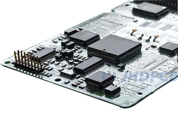
Today’s increasingly complex electronics require more complex, more integrated, and smaller PCB boards, and PCBAs with only one type of component can no longer perform such complex tasks. Therefore, a mixed technology board with both SMD and through-hole components is now required. This type of board comes with through-hole assemblies and SMD assemblies, which requires the collaboration of through-hole technology and surface mount technology. However, soldering is a complex process and tends to be influenced by too many elements. Therefore, it becomes important to better arrange the order of through-hole technology and surface mount technology. There are several type of mixed technologies: Single Side Mixed Assembly, One Side SMT & One Side and THT Double Side Mixed Assembly.

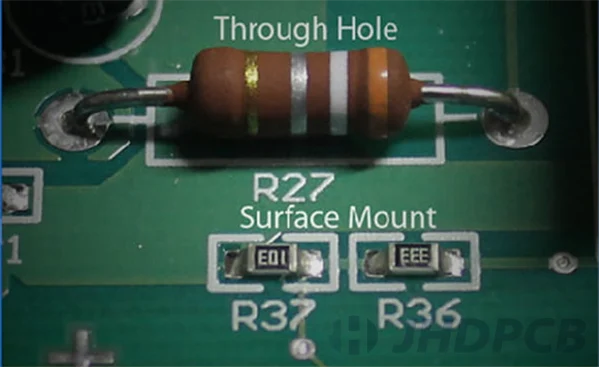
Through-hole Assembly refers to the installation of leads in detail, which are inserted into the holes of the printed circuit board, drilled and soldered on the other side of the pad. This process can be achieved mechanically or manually.

Through-hole assembly2

Mechanical assembly of PCBs including assembling PCB components together in an assembly line. Also, it refers to an assembled part or product made in this way. It combines products to perform specific functions.

Box-build assembly is also known as system integration. A box is a PCB component in a cabinet that is filled with wires, a small enclosure, or a fully integrated electromechanical system with electronic and pneumatic devices.
Adequate package is essential. If you want your PCB to work properly, make sure your manufacturer is using the correct package.

Cable assembly is a group of wires or cables arranged into a single unit. Mostly, cable assembly can transmit power. Also, cable assemblies are used for sending informational signals and provide power to several cables while organizing them in a package that’s easier to maintain and replace.

How to Assemble Multiple PCB boards Together?

In PCB design, we are in a situation where we want to group multiple PCB boards together for various reasons to form a new PCB. There are usually two methods:

Method 1

  1. Open each PCB design you want to combine, one at a time. The schematic may be opened, but we do not process the schematic because the initial design is already complete. Please click to read the complete PCB schematic content.
  2. Go to the Eagle PCBs Layer Settings section and select all layers of the PCB. Select the entire PCB layout and group the entire board design.
  3. Create a new PCB board document.
  4. Copy the PCB design you want to combine (some older versions can’t use the copy option well, just choose Cut), and then paste (or cut) into the new PCB board document you just created, and place the PCB the way you want.
    When merging multiple circuits into a single PCB, the biggest problem can be conflicts between indicators. So: You can look at the hierarchy and channels, and there may be a way to put multiple different circuits into the schematic so that component codes don’t conflict and the PCB can be simply reused.
  5. Generate the document after numbering the boards.
    When assembling boards, you need to be familiar with the manufacturer’s capabilities and capacity, and following the manufacturer’s PCB rules will ensure that your board will be manufactured illegally.

Method 2

Re-annotate the schematic and PCB with a prefix (to get a unique reference indicator between the different circuits), then copy and paste everything into one project.

How to Calculate PCB Assembly cost?

When you first enter the PCB assembly industry, you may find yourself very confused about how to estimate PCB assembly costs. Understanding the total costs involved in PCB assembly can help you complete the budgeting process for your PCB project. Once you know how much it might cost to build a single printed circuit board, you can always look for ways to reduce costs. Also, the total cost of PCB assembly is helpful for you to determine the price of the final product.

Send the document to a reputable PCB manufacturer–
One of the best ways to estimate the cost of PCB assembly is to contact a PCB manufacturer with sufficient industry experience and request a board assembly quote. Ensure that manufacturers have sufficient resources and use the latest technology in SMT. This will make it easy to pick and place components on the PCB with the pick and place machine.
PCB component quotes, manufacturers will usually ask you to provide detailed information about the following areas:

  1. Number of boards;
  2. Bill of materials;
  3. Gerber documents in RS-274X;
  4. Assemble the documentation;
  5. Centroid data;
  6. Any unique specifications;

Make sure to include all required columns when sending the BOM to the manufacturer. Some of the details in the column include indicator, manufacturer name and part number, part description, part quantity, packaging information, etc. If you want to exclude certain parts from the assembly or procurement process, highlight them in the BOM. JHD offers a free document checking service. If your PCB assembly is complex, it is recommended to submit the complete turnkey PCB assembly file for more detailed inspection and advice.

The following factors should also be considered:

  • The material required before assembly. 

    According to the customer’s BOM list, the purchasing department of the processing company will make an inquiry, including PCB bare board, electronic parts, etc. Sometimes, PCB assembly costs and engineering costs are included in the purchase quotation. Due to material losses, such as resistive capacitor disk loading materials and SMT chips, it is necessary to cover about 5% of the material loss when purchasing components. For small batches of PCBAs, the engineering costs are usually included in the quotation, including the costs of machining documents, steel mesh, replacement of SMT lines, etc.

  • Solder joint cost count. PCB assembly costs include post-solder SMT and DIP, etc., which are calculated separately according to the specific conditions and processing methods of the printed circuit board solder joints. Typically, the pad is counted as 1 point, and the number of feet of the IC is calculated. Solder pads with SMD accuracy above 1206 are calculated by 2 points per pad, except for the CD54 inductance count of 12 points, the other large inductor number is 24 points. In addition, one pad with a plug spacing of 3.96 acts as 2 solder joints. After calculating all solder joints, the cost is included in the solder joints between 0.008 and 0.03 yuan.

  • The PCBA test cost based on the test time of each PCBA board.
  • In terms of packaging logistics, special packaging materials and the cost of three anti-paint need to be counted.
  • According to the customer’s trading terms such as FOB, additional customs logistics costs need to be inventoried.
  • PCB assembly cost breakdown.
  • PCB Board Size and Number Layers.
  • PCB Board and Component Material.
  • PCB Board Design Complexity.
  • PCB Assembly Order Volume.
  • PCB Assembly Lead Time.

How to Create a PCB Assembly drawing?

Here are some guidelines to follow for generating PCB drawings that help standardize the process of generating PCB drawings. If you want to make PCB assembly drawings, here are some generic items you should include:

Some CAD PCB drawing systems prompt the user to use a drawing format from the system library. However, other systems automatically generate drawing formats for the user. In either case, the user will combine the drawing format and the PCB layout to generate the drawing.

The board outline represents only the PCB design outline in the layout database. In most cases, this will include:
1. Cutouts;                 2. Slots;
These two components appear on the manufacturing drawing, setting the dimensions. On the other hand, references to these components appear when the drawing reaches the PCB assembly drawing stage.

Within the board outline, you need to display all the part shapes that will be soldered to the board and their reference marks.

You will also need to show any mechanical parts that will be connected to the board through mounting hardware. Because these parts may not be regular PCB packages, you may have to add or draw these shapes separately. An example of such a mechanical component is the catapult handle. This is a non-electrical component that may not be represented in the schematic, but it needs to be included in the assembly drawing and BOM (Bill of materials).

These list of instructions includes basic assembly details, references to industry standards and specifications, and the location of special features.

Your drawing format should have some areas you should take advantage of:

  • Add the identification number of the sheet;
  • It’s revision level;
  • Name of the Board of Directors;
  • Business address;
  • Contact details;
  • Date created.

All of this information helps to uniquely identify your PCB, which is very critical.

1. Component outlines.
When making a PCB assembly drawing, you need to show:

  • shape of each component
  • A reference designator for components in your drawing, based on how soldered this particular board is.

2. Mechanical parts.
You should also include the mechanical parts that attach to the board using the mounting hardware. In some cases, you may need to put in more effort to include these parts in your drawing for the reason that CAD footprint libraries sometimes do not have an accurate representation of these parts. So you have to enter manually.

3. Additional views.
Double-sided boards require a rear view and a front view. As long as the board is not large, these two sides can be placed in one drawing. However, if the board is large, you may need to use additional drawings to cover the entire drawing.
You may also want to add expanded views with details about the mechanical part connections for clarity.

4. Manufacturing labels.
If you include any manufacturing labels such as:

  • Assembly label
  • barcode

Then you have to use the pointer to pinpoint it. Once identified, then cite it in your notes. Anyone looking for it can easily identify it without much effort.

5. Assembly Instructions.
Is a list containing manufacturing instructions, such as

  • Assembly Details
  • Industry Standards
  • Specifications
  • Featured Locations

Assembly instructions sometimes include a parts list, but only when requested by the manufacturer. All these elements can be modified to suit the customer’s specifications. If you think some of these elements don’t work for your client’s drawings, you can even omit them altogether. You should consult your contract manufacturer when selecting the correct elements to use in your drawings. They will tell you what is required to generate the PCB. By doing this, you can avoid duplicating the entire PCB assembly drawing.

What is Turnkey PCB Assembly?

Turnkey PCB assembly is an electronic assembly solution that provides an efficient and cost-effective way to build and test circuit boards for new products with minimal lead times. ‘Turnkey’ refers to a product or service that is ready for immediate use for the buyer. When applied to PCB assembly, this means that the supplier will handle all aspects of the PCB project, which includes the procurement of parts, components and the manufacturing of PCB.
Most entrepreneurs and manufacturers find that old methods of manufacturing electronics and printed circuit board components are slow, error-prone, and expensive. It is not designed for small batch runs and prototyping, nor is it designed to support large orders, and requires a long lead time. When assembling these PCBs, they face certain challenges, such as the need to carry a lot of inventory and have an in-house team to create it.

Turnkey PCB assembly

The turnkey service has become a mainstream trend in China. The turnkey service reduces the time for customers to contact multiple suppliers for each step in PCB assembly manufacturing. The scientific ordering system enables customers to obtain higher quality and lower cost PCB assembly products than traditional PCB assembly methods in a relatively short period of time. The turnkey service allows PCB prototype production to be completed within 12 hours and PCB assembly prototype to be completed within 24 hours to 72 hours, even if there is no minimum quantity requirement. Of course, PCB manufacturing and PCB assembly services can be selected individually or in combination.

How to Find a Reliable PCB Assembly Company?

Six Tips to Find the Best PCB Assembly Companies for You

  • Identify Your Unique Needs;
  • Follow an appropriate Timeline;
  • Weigh Experience;
  • Verify Quality Control;
  • Compare Costs;
  • Look for Synergistic Relationships.

Current status of PCB assembly

* It is difficult for European and American manufacturers to satisfy PCB assembly.

First of all, high cost and long delivery time have always been the concerns of European and American customers for PCB assembly prototypes. Because local PCB manufacturers are limited and cannot keep up with market demand, few manufacturers can provide one-stop PCB assembly services. If customers carry out PCB assembly in their own country, it may cost more money and time.
In addition, differences in language and culture make it difficult for customers to assemble PCBs abroad. For example, many foreign trade companies can provide PCB assembly services. But there are not many people who are good at foreign languages ​​and PCB manufacturing technology at the same time. Therefore, finding the right PCB manufacturer is not easy.

* The turnkey service of PCB assembly has become a mainstream trend in China.

In order to meet the increasing demand and improve market competition, many PCB assembly manufacturers provide turnkey services for domestic and foreign customers. For example, JHDPCB is a professional PCB manufacturer. With years of accumulated experience and excellent engineers, it can provide customers all over the world with one-stop service from PCB manufacturing to assembly.


If you are looking for a high-quality fast turnaround PCB assembly solutions provider, please choose us. We can meet your various needs.
With many years of accumulated experience and excellent engineers, JHDPCB can provide one-stop service from PCB manufacturing to assembly for customers around the world. For more PCBA production capabilities and the advantages of the CSA, please refer to the JHDPCB. Advanced equipment, high-quality materials, experienced engineers and punctual delivery are important factors for excellent one-stop PCB manufacturers. JHDPCB has complete and efficient assembly solution. We are able to deliver faster in the field of light PCB assembly special packaging. As an experienced PCB prototype manufacturer, providing turnkey PCB assembly services, JHDPCB can provide cost-effective solutions for different needs while ensuring quality. JHDPCB’s sales staff also received training in PCB manufacturing expertise to effectively solve technical communication problems with customers.

Get a PCB Quote Now

Open high-quality PCB manufacturing services in JHDPCB