Why choose JHDPCB?
- Real PCB and PCBA manufacturers;
- Meet industry certification and production standards;
- 99.48% delivery on time;
- 10+ years of industry experience;
- 150+ experienced R&D team;
- 3000+ orders/day;
contact us
Provide quality service for your PCB project. Tel: +86 755 2753 9533
PCB Quality Control
JHDPCB is definitely your trusted PCB & PCBA partner! We make every effort to improve our products, services and processes to meet or exceed customer expectations. To create the highest quality PCB products and services for customers, we pursue continuous innovation of products as the driving force, actively pursue quality and reliability, and improve the overall satisfaction of customers. Therefore, quality control is an important part of our production process.Quality assurance is implemented in all aspects, including:
Through Authoritative Certification--
JHDPCB has its own PCB manufacturing factory certified by UL, ISO 9001:2015. At the same time, all employees in the manufacturing process will pass IPC training, JHD will have a certified IPC trainer on site, which will enable our employees to keep up with the required biennial IPC certification. Ensuring the highest level of manufacturing quality for our customers, IPC certification ensures that all employees work to the same requirements and standards, always ensuring that all products are of exceptional quality, reliability and consistency. Products will have better performance and longer service life under the condition of lead-free regulations.
PCB Files Inspection Before Production --
For each order submitted on JHDPCB, the PCB file will be reviewed by our professional engineers before being sent to production. Engineers will confirm the feasibility of the design in terms of tolerance limits such as board edge clearance, drilling,pad spacing and wiring. When the engineer finds any problem in the file or there any places can be optimized ,they will issue an EQ and our sales will get in touch with you to avoid delays in production.
Raw Material Guarantee--
It is always known that the quality of raw materials determines the durability of the finished product. Ensuring the high quality of raw materials is one of the most basic principles of JHDPCB manufacturing products. JHDPCB has been cooperating with leading suppliers in the industry. We use top-level materials, such as Bergquist,Rogers,KB and Goldmax laminate; TAIYO high resist performance solder mask.
In addition to ensuring that high-quality materials are used in the circuit board itself, other component sourcing also requires good quality control. Because any delay in sourcing components can result in a stall in the PCB manufacturing process or a change in the intended production design. To minimize potential problems, JHDPCB takes the following QC steps:
BOM Verification – These checks ensure that the components in the BOM match the PCB design.
Component Reference Designator Validation – This is a unique identifier in the BOM. If this is incorrect, the number of components fetched may be wrong.
Manufacturer Part Number (MPN) Verification – The MPN may be incorrect and may result in obtaining the wrong component. An incorrect number may result in the wrong package type. This error results in lost time and additional costs.
Component Manufacturing Status Check – This ensures that components are in good condition for production.
Component Tolerance Check – This test ensures that the component actually meets the data sheet tolerance range.
Solderability Testing – This is an accelerated “aging” process applied to samples to determine solderability.
Kit Accuracy – Inaccurate kit components will result in significant delays and additional costs.
MPN – Package Matching – Avoids component and package mismatch where errors can violate solder relief and component spacing requirements.
Documentation Review – Review component shipping documentation for errors.
Visual Inspection – This helps ensure components match your order and documentation.
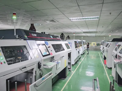
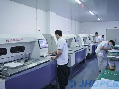
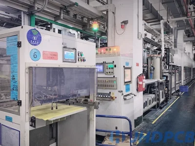
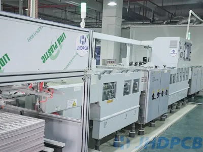
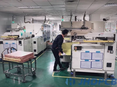
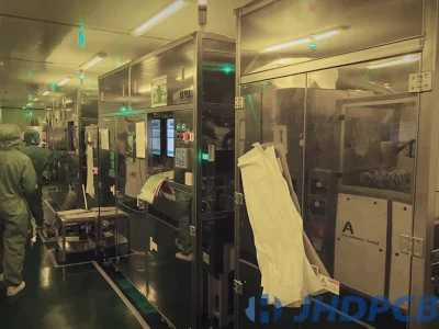
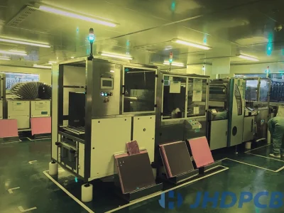
The World's Leading Production Equipment --
In order to ensure the best quality and reliability of PCB products, JHDPCB continues to invest in the introduction of advanced equipment, including but not limited to the following:
- Lamination machines from VIGOR Orbotech&HANS .
- LDI Machines from Orbotech&HANS
- Fully etching lines from UCE
- VCP Copper plating lines from UCE & Command
- Fully spray coating lines from FUJI
- Mechanical drilling machines from SCHMOLL,HITACHI&HANS
- Laser drilling machines from Mitsubishi
- AOI machines from Orbotech
- Automatical E-tester machine from Mason
Process Control--
All production processes comply with IPC standards. ISO regulations for quality control processes, risk management and traceability, detailing the step-by-step process of PCB assembly. In addition, we have well-documented process controls to control the quality of the manufacturing process by regulating soldering temperature, shelf life and cleanliness standards.
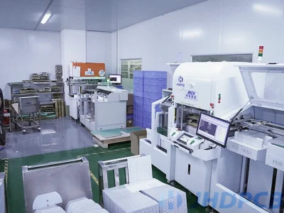
Quality Inspection Before Shipment--
AOI (Automatic Optical Inspection)
AOI test after pattern plating. AOI automatic optical inspection is based on the principle of optics, using a combination of image analysis, computer and automatic control technology, using a camera to scan the circuit board with extremely fine details, and compare the webcam PCB image with the image of the “perfect” circuit board to check Connections and soldering quality for defects or failures. In order to improve the accuracy of AOI testing, JHDPCB introduced advanced AOI from Orbotech to prevent bad PCB from flowing to the next process.However, AOI cannot check vias, so flying probe test or E-tester fixture is also necessary
Flying probe test
This kind of electrical testing uses electromechanical control probes to access the components on the circuit board, and the test probes move quickly point by point on the PCB circuit board to complete the test. The moving position of each test probe is controlled by a precision transmission system, and the position accuracy can reach 0.01mm. Although the flying probe test can accurately detect whether the PCB is short-circuited or non-conducting, the flying probe need to check the signal one by one, the test speed is relatively slow, the whole testing time usually takes 1-3 minutes. So flying probe only suitable for small-volume PCB orders.
The electrical test
The electrical test have become an irreplaceable test method for PCBs with blind vias and buried vias. Because AOI can not check the vias but E-test can check out the missing connections on the board.The electrical test needs a specific tool for fixture test, we called it E-tester. The E-tester is generally designed according to PCB panel, and it is covered with test pins, can test a complete panel within 1 minute, which greatly improves the test efficiency and is suitable for bulk order. JHDPCB has introduced the latest testing machine from MASON, as long as the E-tester is ready, the PCB can be tested without errors.
X-rays
X-rays provide a non-invasive but expensive way to check for proper PCB assembly, providing non-invasive high-quality imaging of the internal quality of the PCB.
Saw
Cutting a PCB with a saw can be destructive to individual boards, but can provide a valuable reference to the larger picture of the entire assembly process. This test is mainly used to check through holes. Recommended only for mass production runs.
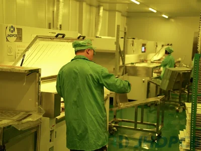
Manual inspection
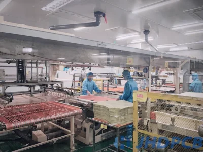
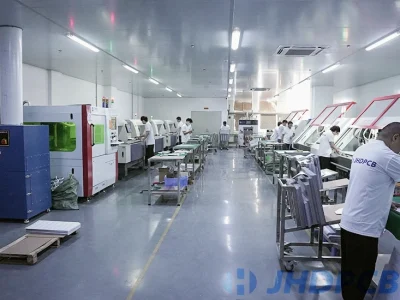
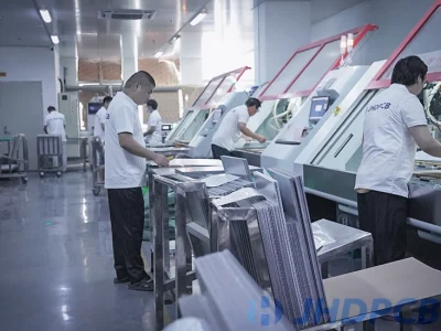
In addition to machine testing, we are also equipped with quality inspectors in each production link. We regularly train quality inspectors to make them understand the IPC-A-600 product acceptance standards.From IQC inspection of raw materials to OQC inspection of shipments, the cooperation of inspection equipment and labor can greatly reduce defects.At the same time, we also set up a special quality inspection department to inspect each PCB with the naked eye before shipment. In this way, some problems that cannot be found by the machine can be checked, such as some defects in the shape or solder mask.
Vision
For low volume production, have someone (usually the person performing the assembly) briefly observe it with their own eyes throughout the assembly process. It doesn’t just mean quick browsing. They must double-check every connection in a well-lit environment. to check for excess solder, unconnected components, and other issues that may require rework.
Microscope
To reduce stress on the eyes, inspectors can use hand-held optical tools such as magnifying glasses or microscopes to project PCB connections onto a large screen for detailed inspection for a closer look. Often used to improve visual inspection.
Functional Testing
This testing method is essentially a full commissioning after PCB fabrication. The operator powers up the PCB and programs it to perform a series of self-tests.
More information on PCB testing can be found in.
JHDPCB has passed IPC Class 3 standards, ISO9001:2015, UL, ROHS, REACH certification, and has developed a strict and complete quality management system. In addition to the basic visual inspection, all circuit boards undergo the most stringent functional tests. We use industry-renowned testing and inspection equipment, such as MASON flying probe tester, OXFORD X-ray inspection machine and Orbotech automatic optical inspection (AOI) machine. We guarantee that every PCB to your hand will be good, and you can safely carry out the next step of assembly. If you find any quality problems during use, please get in touch with sales@jhdpcb.com in time, we will solve your problem as soon as possible.


