Comprehensive Understanding Of Multi Layers PCB
The definition of a multi-layer PCB is a PCB made of three or more layers of conductive copper foil. It’s equivalent to the upgraded version of single-sided PCB.

What is Multi-Layer PCB?
In the case of a large number of interconnection and crossover requirements, if the PCB circuit board wants to achieve a satisfactory performance, it must expand the board layer to more than 2 layers. Therefore, the original intention of the multi layer circuit board has appeared. It provides more freedom for the routing path.
The multi-layer circuit board has a layer of core material, and the copper layers are sequentially laminated on both sides using insulating prepreg. Multilayer boards typically contain three or more copper conductive layers. The top and bottom layers look similar to a double-sided PCB, but have many circuit layers in the center. Internal layers with plated holes for interconnection (through, blind, buried). The copper layers are bonded together by a resin layer (prepreg, PP). Various IC electronic components are soldered on top or bottom layers of multilayer circuit boards by using different packaging techniques such as SMT and BGA.
The manufacturing process of multilayer circuit boards is more complicated and more expensive than single-sided and double-sided PCBs, and the cost of troubleshooting is high. But multilayer printed circuit boards support high-density wiring designs. There is no limit to the number of layers in a multi-layer PCB, which depends on the manufacturer’s production capacity. The thickness of the board will increase with the increase of the number of layers of the circuit board, so as to meet the diversified circuit design and packaging process for a wider range of applications. The number of layers of a multi-layer PCB is usually superimposed by an even number, and the manufacturing cost of the odd-numbered layers will increase significantly and problems such as rockers are prone to occur.

Our Advantages in multilayer PCBs
The world’s leading production equipments:We have introduced a variety of world-renowned production equipment, such as Orbotech LDI, VIGOR lamination machines, Mitsubishi laser drilling machines, Command plating lines, PTH Lines and etc.
Excellent procurement supply chain management: We reduce our material costs through centralized procurement and large-scale procurement.
Experienced team of experts: We have been deeply engaged in multilayer circuit board production for more than 12 years and grow into an industry-leading multilayer circuit board manufacturer, supported by an experienced team of experts that can provide our customers with reliable quality PCB.
Quick delivery: To shorten the delivery time. Everything is manufactured under one roof with our state-of-the-art equipment. We have many brands of laminate in stock, such as aluminum. Can deliver 3-5 days for sample order and 14-18 days for bulk order. More lead times can be found in “PCB Quick Turn”.
Rich experience in projects: Over the years, we have served various multi-layer projects in various industries, and manufactured the highest quality PCB projects for virtually every technology company, and we can do the same for you.
View information about JHD’s manufacturing plants.
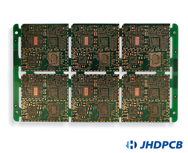
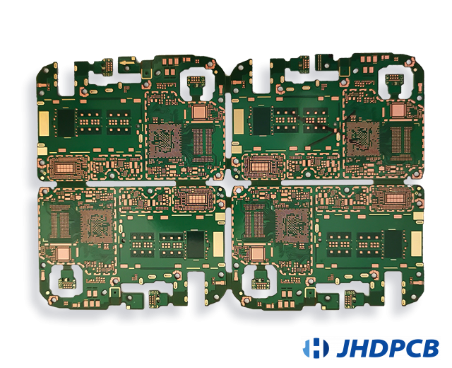
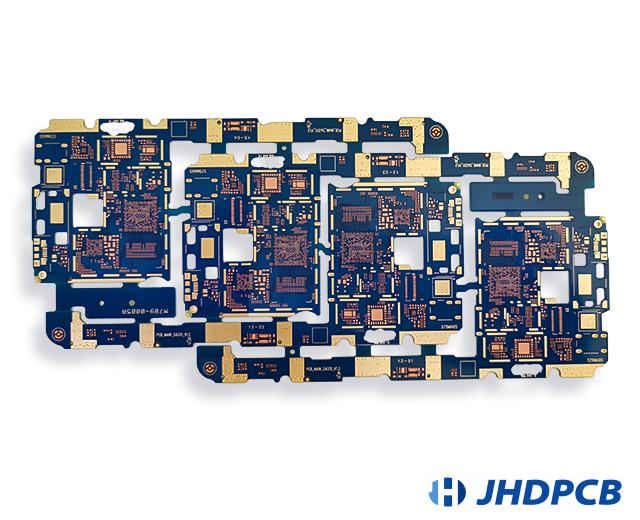
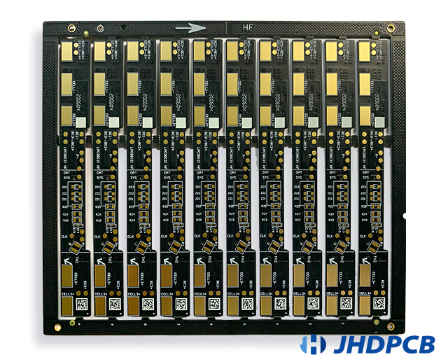
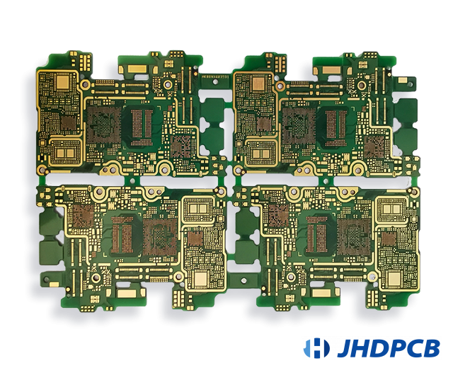
JHDPCB Related Multilayer PCB Board Product Case Display:
JHD's multilayer PCB manufacturing capabilities.
| Item Content | Description |
|---|---|
| Layer Counts: | Mass production: 30; Sample: 64; |
| Material type: | FR-1, FR-4,CEM-3,Copper base, Aluminum,Polyimide(PI) |
| Surface finish: | ENIG gold, HASL(LF),OSP, Immersion Silver,Immersion Tin, Electroplated nickel gold,,ENEPIG |
| Trace thickness: | T≤1.0 / 1.0 / 1.6 / 2.5 / T≥3.2 |
| Trace Thickness Tolerance: | ±0.10 / ±0.13 / ±0.18 / ±0.23 / ±8% |
| Minimum Core Thickness: | .001″ |
| Drill Aspect Ratio: | 35:1 |
| Minimum Drilled Hole: | .002″ |
| Min space/width: | 0.1mm |
| Warp and Twist: | ≤0.5%(board thickness:1.6mm,PCB size : 300mm*300mm) |
| Outline Tolerance: | ±0.15mm |
| V-CUT Precision: | ±0.1mm |
| Capacity: | 80000㎡/Month |
| PTH Dia tolerance: | ±0.076mm |
| Outline tolerance: | CNC :±0.1mm punch:±0.15mm |
| Min.Solder Mask Bridge: | 4mil |
| Min.Line/Track Width: | 3mil |
| MIN.Drilling Slot Size: | 0.6mm |
| Solder Mask Color: | Green, Black, Blue, White, Yellow, and Matt, etc. |
| Solder Mask Hardness: | 6H |
| Flammability: | 94v-0 |
| Turn hole: | Blind vias, buried vias, micro vias, through vias |
| Finished Copper Thickness: | 0.5 – 20 OZ |
| Other Technology: | Gold Finger, Peelable Mask, Non-across Blind-Buried vias, Characteristic Impedance Control, Rigid-Flex Board etc. |
Check Out The JHD Multi Layer PCB Production Line Video:
directory
How to make multi-layer pcb?
After the multi-layer PCB design is completed, it is first necessary to use a series of techniques such as UV exposure and etching to make the required inner core.
Then there’s lamination. The layers of prepreg and core material are alternately laminated together using a high temperature hydraulic press to create a multi-layer PCB. Prepreg and core are essentially the same material, but the prepreg is not fully cured, making it more ductile than the core. During the lamination process at high temperature and pressure, the prepreg is caused to “melt” and join the layers together. Multiple layers of prepreg and core material are laminated together under high temperature and pressure. After cooling, a very strong multilayer circuit board is obtained. This process ensures that there is no air between the inner layers. The circuit traces are completely encapsulated by resin. Material combinations range widely, from basic FR-4 to special ceramic or high TG materials.
Normally, electronic components would be assembled on the outer layers of a multilayer PCB. This facilitates soldering and disassembly/replacement of later components. However, in some complex medical, military, and aerospace applications, ICs may be placed in layers inside the PCB. In order to reasonably distribute the power supply layer and the signal layer, avoid electromagnetic interference.
Additional circuit traces can also be added to the top and bottom layers if necessary. Then it is to combine the packaging process requirements and application scenarios of the circuit board to do the surface treatment and the spraying of the conformal paint. So far, a complete multi-layer PCB bare board has been completed.
How to design multilayer PCB board?
Due to the circuit complexity of multilayer PCBs, we also need special attention during the design process. The copper traces on the PCB allow current to pass, and the width and height of the copper traces and the level of the prepreg will affect the signal transmission of the current. This is why impedance control is required. Avoid adverse effects such as undershoot, overshoot, crosstalk, coupling and electromagnetic interference for normal use. Good design can ensure smooth multi-layer PCB manufacturing and reduce costs. The following are JHD’s design recommendations based on past experience:
- The power plane is always in the middle of the board, and the ground wire is closer to the top layer. After the power supply of the inner layer is processed, the remaining space is available for the routing signal tracks. For example, in an eight-layer board stack, there will be six layers of signal circuits and two layers dedicated to power.
- Reasonable use of through holes, blind holes and buried holes for point connection of different layers. (Click to read the detailed knowledge of PCB hole types)
- Multilayer PCBs with more than 8 layers are usually rigid PCBs. Design formats for flexible PCBs should be avoided.
- Theoretically, the number of layers of a multilayer PCB is infinite, but in conventional use, in order to control the overall thickness of the circuit board. It is usually recommended to control below 30 layers.
- When the circuit in a multilayer PCB belongs to DC (low frequency), its design is very easy. And if it belongs to high frequency work, you need to consider the influence of electricity, physics and magnetism. In order to maintain the good operation of the circuit in practical application.
- Reasonably locate the “low frequency layer”, “high frequency layer”, “power layer” and “ground layer”. The insulating layer and the signal layer are always kept parallel. These two points can effectively carry out impedance control to avoid bad signal transmission.
Why do we need multilayer circuit board?
Over the past few decades, electronic devices have become more widespread. All electronic products are developing rapidly and getting smarter and smaller. For example, the mobile phone is not limited to making calls and texting chat, it integrates the work that can be done by a computer. Home control panels are not limited to simple light switches, but include light brightness and warm and cool color temperature adjustment. It can even control supplies such as air conditioners, stereos, curtains, etc.
All of this requires a multi-layer PCB for miniaturized fine circuit control. The internal components of all electronic products are following the trend of miniaturization and multi-functionalization. Multilayer PCBs allow more circuit routing and the integration of a large number of IC components in a limited space. It plays an important role in the functional control of the entire electronic system.
Features of multilayer PCBs.
What Are The Advantages Of Multilayer Printed Circuit Board?
Although the process of designing a multilayer PCB is complex and requires designers and manufacturers to be proficient in the field. But the product advantages they offer are definitely worth it. Here are some benefits of multilayer PCBs:
Increase the durability of PCB: Due to the heat and pressure used to bond the layers together during the manufacturing process of multilayer PCBs. So it is inherently very durable. The more layers, the thicker the circuit board, so it is more durable than single-sided or double-sided PCB. This increased durability means that circuit boards can withstand harsher conditions and generally have a longer lifespan.
Small size: Multilayer PCBs achieve this enhanced durability while still maintaining relatively small size and low weight. Because they stack layers together, you can squeeze more functionality into a more compact space than other boards. This smaller size also means less weight. Single-layer boards must be large to match the functionality of multi-layer boards. The most prominent advantage of using a multilayer PCB is that it enables more circuit interconnections in a small size. Evolving manufacturing processes and advanced design rules are constantly helping multilayer PCBs reduce board size. Multilayer PCBs are suitable for smartphones and electronics that require a small form factor, so they can easily accommodate the growing demand for electronic wearables.
Lightweight: Due to the small size of a multilayer printed circuit board, it is usually very light. Due to its lightweight properties, multilayer PCBs are popular in handheld medical devices and wearable smart devices. One of the prominent reasons for the weight reduction is the elimination of the multiple connectors required for separate double-sided PCBs that interconnect multilayer designs.
Suitable for more complex projects: Projects that are more complex and involve more circuits and components often require the use of multilayer PCBs. This is all thanks to a lot of work in its design and manufacturing process. to increase the versatility of multilayer printed circuit boards. Because single-layer boards do not have enough space to implement complex circuit designs, one can increase the space by adding layers. The multi-layer pcb design ensures plenty of room for connections, making it ideal for more advanced devices.
Attachable Flexibility: At some point, we can add flex circuit construction on a multi-layer PCB. That is, soft and hard combined PCB. They provide a base of flexible application and do not require a complete redesign. Of course, this is not suitable for all multilayer PCBs. The higher the number of layers, the lower the bendability of the flexible construction.
High packaging efficiency: The multi-layer feature of multi-layer PCB allows it to add more electronic components in the same space. View detailed PCB assembly information.
Single Connection Point: Multilayer PCBs are designed as a single unit of work and do not need to be connected in series with other PCB components. Therefore, a multilayer circuit board has only one connection point. This plays a major role in helping PCBs achieve miniaturization.
Higher Quality: The design and production of multi-layer circuit boards require more professional production knowledge and more advanced production lines, which increases your possibility of obtaining high-quality products. Many of the multilayer printed circuit board designs include advanced controlled impedance characteristics and electromagnetic interference shielding to further improve performance.
Disadvantages of Multilayer PCBs.
Higher manufacturing costs: Multilayer boards are more expensive than single-sided and double-sided PCBs at every stage of the manufacturing process due to their circuit complexity. They require a lot of time during the design phase to address all potential issues. A large amount of time and labor is required to perform highly complex manufacturing processes. JHDPCB from China provides competitive prices to help many customers complete multi-layer PCB manufacturing at economical prices.
More Manufacturing Time: Multilayer circuit boards require more manufacturing time than single- and double-sided PCBs. Because it needs to perform more processes such as etching, lamination and electroplating. The higher the complexity and number of multilayer circuit boards, the longer the manufacturing cycle required. Click to view the standard lead time of JHD Multilayer PCB.
More difficult to repair: The assembly position and structure of electronic components need to be preset in advance in the multi-layer PCB design process. Compared with ordinary single-sided and double-sided PCBs, it is more difficult to debug and repair when errors occur later. For more repair information, please visit The Ultimate Guide To PCB Repair And Rework.
What Are The Applications Of Multi-Layer PCBs?
Medical equipment: Electronic devices are an indispensable part of the medical industry. Like any other industry that relies on electronics, the medical industry is also adopting miniaturization. With the popularization of non-invasive treatment technologies, the medical industry has an increasing demand for micro-devices. Multilayer printed circuit boards can perfectly meet the needs of these devices due to their small size, lightweight design and other powerful features. Some of the best examples of medical devices using multilayer PCs include X-ray equipment, CAT scanning equipment, blood pressure and blood sugar testing equipment, MRI, CT scanning, infrared temperature monitoring, etc.
Consumer electronic products: Consumer electronics, usually called household electronics, cover a wide range of electronic devices for daily use. This often includes devices used for communication, such as smart phones, laptops, etc.; entertainment, including smart TVs, music players; and kitchen appliances-microwave ovens, washing machines, etc. Most of these devices are equipped with multilayer printed circuit boards instead of standard single-layer PCBs. why? This is because the multi-layer PCB contributes to its functionality and compact design.
Industrial electronics: Electronic equipment used in an industrial environment is very different from consumer electronics. The reason is that they are exposed to harsh environments such as high temperature, shock, vibration, pressure, dust and humidity. Some common examples of industrial electronic equipment include automated assembly lines, packaging conveyors, painting robots, etc. They are designed for long-term operation and can work throughout the day. In this case, a durable PCB is required, and a multilayer PCB meets this requirement. Multilayer PCBs are more durable than other alternatives on the market today.
Computers and equipment: Today, we cannot imagine life without computers and automation. Due to its space-saving and functional features, all products of computers and related products (such as graphics cards, motherboards, computer mice, etc.) use multilayer PCBs. These PCBs can be designed to achieve superior performance at a lower cost than other competing technologies.
Telecommunications Electronics: Multilayer PCBs are used in many telecommunications equipment, such as GPS and satellite applications, and signal transmission. These equipment require durability while maintaining a high level of functionality. With the development of wireless technology, the demand for high-performance and precise micro-devices is increasing. Multi-layer PCB can easily meet the requirements. Other applications of telecommunications electronics include communication towers, radar electronics, power amplifiers, attenuators, and so on.
Military, aerospace, and Defense: Similar to the above industries, multilayer PCBs are becoming a priority for many military and defense applications. These PCBs have compact design, low weight, functionality and durability, and are high-speed devices. Unmanned ground vehicles (UGV), aircraft defense systems and avionics, unmanned aerial vehicles (UAV), surveillance, automatic guns, and radar systems are some of the devices equipped with multilayer PCBs. In order to meet the strict requirements of high circuits, multi-layer PCBs are assembled with military specification components to withstand the harsh environment where high temperature and high pressure may cause damage to grade components. JHD has a complete and rigorous PCB testing program to detect all possible defects as much as possible. In order to ensure that every order that customers hand to us can be applied perfectly.
What are the pain points of multi-layer PCB manufacturing?
Although multi-layer PCB has unparalleled product advantages, there are still technical difficulties in the design and production process. Let’s take a look at the problems that will be faced when choosing a multi-layer printed circuit board:
- Material requirements:
Poor multi-layer PCB substrates and incorrectly chosen materials can degrade performance, increase emissions and crosstalk, making them more susceptible to external noise. High-quality PCB board substrates can effectively reduce electromagnetic radiation and crosstalk, and can also improve signal integrity to provide low-inductance power. The superior designability of a multi-layer PCB stack-up can improve RF field immunity by a factor of 10 or more compared to double-sided boards.The choice of laminate and substrate also depends on the type of application and the number of active and passive components to be mounted. - Impedance control of internal layers:
Multilayer PCBs have many circuit layers to improve electromagnetic compatibility (EMI) and ensure signal integrity. The prepreg between all signal layers must remain flat. Tight coupling between layers can reduce impedance, which in turn reduces common-mode radiation between board circuits and reduces signal crosstalk. - Complex design process:
Designing a multi-layer PCB takes more time and designers need to follow many design rules. - Higher expertise required:
Not just anyone can design a multilayer PCB. They need to be proficient in PCB design tools such as Altium design, Eagle, KiCad and CAD, and have a solid understanding of multi-layer PCB stack-up design rule checking. Likewise, not all PCB manufacturing plants are capable of manufacturing multi-layer circuit boards. Multilayer PCBs have strict requirements on the professionalism of the manufacturer’s engineering team, production equipment and quality control of the manufacturing process. Therefore, designers and manufacturers are very important in the field of multilayer PCB expertise. - Complicated production:
Any small design or manufacturing flaw in a multilayer PCB can render it useless. This requires more rigorous manufacturing techniques and high-precision production equipment.
JHD has many years of experience in PCB manufacturing. Standardized production tolerances, strict quality control systems and regular staff training have helped many of our customers to perfectly land multilayer printed circuit boards. Click to see more about JHD’s capabilities and factory equipment.
For more product information or any related PCB project needs, please contact us via live chat, or contact JHDPCB customer service staff by email. We provide free PCB file inspection to help customers achieve more efficient PCB production with the most economical production solution. JHDPCB will do its best to help our customers maximize their benefits with professional and ingenuity.


