| Additive Process |
The process of adding conductive material to a base material, whether it be coated or uncoated, is known as deposition or addition. |
| Ambient |
This refers to the conditions in which a system or component is exposed to contact with its external surroundings. |
| Annular Ring |
This refers to the conductive material encircling a hole in its entirety. |
| Anti-Tarnish |
A chemical treatment process performed after a procedure, used to prevent or impede the oxidation of copper circuits. |
| Array |
This refers to an assemblage of components or circuits which have been organized in a grid pattern on a substrate. |
| Artwork |
This refers to a precisely proportioned layout of electronic information utilized in the creation of an artwork or production master. |
| Artwork Master |
This refers to a photographic representation of the printed circuit board pattern on film, which is employed in the production of the circuit board, usually at a 1:1 scale. |
| Aspect Ratio |
This refers to the aspect ratio of a printed circuit board, which represents the relationship between its thickness and the size of the smallest hole it contains. |
| B-Stage |
This refers to a stage in the chemical reaction of a thermosetting resin, whereupon heating the material undergoes partial softening and swelling, without complete melting or dissolving, when exposed to specific liquids. |
| Backup Material |
This refers to a rigid and flat substance utilized as support when drilling through laminate material, with the goal of minimizing any jagged edges or unevenness. |
| Backplane |
This refers to an extensively sized printed circuit board designed to accommodate a multitude of pins for the purpose of wire wrapping. |
| Barrel |
This refers to the tube created by coating the interior of a drilled hole through the process of plating. |
| Bare Board |
This refers to a printed circuit board that has not yet been fully assembled, including the absence of any electronic components. |
| Base Material |
This refers to the non-conductive substance utilized for shaping the conductive design on a circuit board, which can have both rigid and flexible properties. It may also take the form of either a dielectric or an insulated sheet of metal. |
| Base Material Thickness |
This refers to the thickness of the substrate material, not including any metal foil or surface coatings deposited upon it. |
| Bed of Nails |
This refers to a testing device comprised of a frame and a receptacle containing an array of spring-loaded pins that establish electrical connectivity with a flat test object. |
| Blind Via |
This describes a via that passes through only one surface of a printed circuit board and does not extend between the top and bottom layers. |
| Blister |
This refers to a specific area of swelling and/or separation that occurs between any of the layers of a laminated substrate material, or between the substrate material and conductive foil, and is a type of delamination. |
| Blanking Die |
This refers to the process of using a die punch to “blank out” or cut the completed circuit board, which is primarily utilized for single-sided panels. |
| Blow Holes |
This describes the presence of blow holes that result from a burst of gas emanating from the solder fillet on a circuit board during the soldering process. |
| Board Thickness |
This refers to the total thickness of the substrate material and all conductive materials deposited on it. |
| Book |
This refers to a designated quantity of prepreg layers that are combined with inner-layer cores prior to being cured in a lamination press. |
| Bond Strength |
This defines the interlayer peel strength of a circuit board, which denotes the force required to delaminate two adjacent layers of the board in a direction perpendicular to the board surface per unit area. |
| Bow |
This refers to the degree of non-flatness of a circuit board, which is characterized by a somewhat cylindrical or spherical curvature that results in the four corners of the rectangular product lying on a common plane. |
| Border Area |
The excess base material surrounding the edges of the final product being produced is referred to as the panel margin or panel border. |
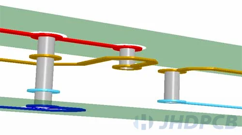
| Buried Via |
A hole that is drilled through the internal layers of a multilayer circuit board but does not penetrate the outermost layers. |
| Burr |
A raised edge or bump that encircles a hole on the outer copper surface resulting from the drilling process. |
| C-Stage |
A dielectric material that has been completely cured to its final state. |
| C-Stage Resin |
A cured resin that has achieved its final level of curing. |
| CAM– (Computer Aided Manufacturing) |
The utilization of computer systems, software programs, and procedures that involve human operators in decision-making during different stages of the manufacturing process while computers provide functions to manipulate data. |
| CAM Files |
The data files utilized directly in the production of printed circuit boards. The file formats include: (1) Gerber data, which governs a photoplotter. (2) NC Drill data, which governs an NC Drill machine. (3) Digital drawings in formats such as Gerber, HPGL, or any other compatible format used for the manufacturing of printed circuit boards.Physical copies of prints may also be available. Computer-aided manufacturing (CAM) files represent the final outcome of PCB design. These files are provided to the PCB manufacturer, who further refines and manipulates the CAM data in their processes, such as in step-and-repeat panelization. |
| Card |
A synonym for a printed circuit board is a circuit card. |
| Capacitance |
The characteristic of a system comprising dielectrics and conductors that permits the retention of electrical charge when voltage is present between the conductors. |
| Catalyst |
A substance employed to start or accelerate the reaction between a curing agent and a resin. |
| Caul Plates |
Stable, flat, polished steel plates that are inflexible in nature and are used during the lamination or pressing of multilayer printed circuit boards. |
| Center to Center Spacing |
The rough estimate of the distance between the central points of neighboring elements on a single layer of a printed circuit board, including surface mounts and gold fingers, is known as the pitch. |
| Circuit |
An assembly of electrical components and devices that have been linked together to accomplish a specific electrical purpose. |
| Clad |
A copper structure present on a printed circuit board. When designating particular text elements as “in clad,” it indicates that the text must be made of copper rather than silkscreen. |
| Overlay |
A state in which a thin sheet or layer of metal foil has been attached to one or both sides of a substrate material. |
| Clearance Hole |
A hole within the conductive design that is larger in size and aligned with a hole present in the base material of a printed circuit board. |
| Component |
One of the fundamental components utilized in constructing electronic devices, such as resistors, capacitors, connectors, DIPs, etc. |
| Component Hole |
A drilling on a printed circuit board utilized for securing and/or electrically linking component terminals, such as wires and pins. |
| Component Side |
The layer of the printed circuit board where most of the components are placed, also referred to as the component layer or the front layer. |
| Conductive Pattern |
The pattern or configuration of the conductive material on a substrate material, which includes conductors, pads, holes, heat dissipation structures, and passive components when they are integral to the fabrication process of the printed circuit board. |
| Conductor Spacing |
The visible measurement between the neighboring edges (excluding center-to-center spacing) of individual patterns within a conductor layer. |
| Continuity |
A continuous route for the passage of electric current within a circuit. |
| Conformal Coating |
A conformal coating is a layer of protective and insulating material that conforms to the shape of the assembled printed circuit board and is applied as a final step in the manufacturing process. |
| Connection |
A single branch of a net. |
| Connector |
A connector or socket that can be effortlessly connected to or disconnected from its counterpart. Multi-contact connectors unite two or more conductors with others to form a single mechanical assembly. |
| Controlled Impedance |
The process of aligning substrate material characteristics with trace dimensions and positions to generate a precise electrical impedance for a signal as it travels along a trace. |
| Crosshatching |
The division of a sizable conductive area through the utilization of a void pattern within the conductive material. |
| CTE – (Coefficient of Thermal Expansion) |
The assessment of how much a material alters in any axis for each degree of alteration in temperature. |
| Curing |
The process of utilizing temperature and pressure to affix laminate materials together. |
| Database |
A group of correlated data elements kept together in a non-repetitive manner to support one or multiple applications. |
| Date Code |
The process of labeling merchandise to indicate the date of its production, following the ACI standard of WWYY (week week year year). |
| Datum |
The precise hypothetical spot, axis, or plane that acts as the reference point for determining the position of geometric attributes of features of a component. |
| Delamination |
The division of layers within a substrate material, between a substrate material and a conducting foil, or any other flat division present in a printed circuit board. |
| DES |
The procedure of developing, etching, and stripping employed in the etching stage of manufacturing inner layers. |
| Design Rule Checking |
The utilization of a computer-assisted software to conduct continuity confirmation of all conductive pathways routing in compliance with relevant design principles. |
| Desmear |
The elimination of melted resin caused by friction and debris resulting from the drilling process, from the wall of a drilled hole. |
| Dewetting |
This refers to a situation where a surface has been covered by molten solder and subsequently withdrawn, resulting in unevenly shaped bumps separated by thin areas of solder. The underlying material remains concealed. |
| Dielectric |
An element possessing a significant impediment to the passage of electricity and the ability to become polarized by an electric field. |
| Dimensional Stability |
A metric of the alteration in size of a substance resulting from various factors such as variations in temperature, humidity, chemical treatment, and stress exposure. |
| Dimensioned Hole |
A perforation in a printed circuit board whose position is established by physical measurements or coordinate values that may not align perfectly with the designated grid. |
| Direct Plate |
The process of depositing conductive coatings onto drilled holes to ensure electrical connectivity for electrolytic plating. |
| DOE |
Experimental design… a structured approach to developing an interactive test plan. |
| Dog Bone |
A deficiency in plating observed in drilled holes where the copper electroplating is thinner at the center and thicker at the edges. |
| Double-Sided Board |
A double-sided printed circuit board is a type of circuit board that has conductive traces and features on both top and bottom surfaces.
“Double-Track” is a colloquial term used to describe a narrow design involving two traces between dual inline package (DIP) pins. |
| Double Treat |
A coating made of brass applied to copper foil in place of oxide. |
| Dry-Film Resists |
A type of coating material formulated for the fabrication of printed circuit boards and chemically-machined components that effectively withstands a range of electroplating and etching procedures. |
| Dry Film Solder Mask |
A photo-imaged solder mask film that is applied to a circuit board, capable of accommodating the higher precision demanded by surface mount technology and fine line designs. |
| Electrod Eposition |
The process of depositing a conductive substance from a solution used in plating through the use of electrical charge or current. |
| Electro Less Deposition |
Auto-catalytic plating, also known as electroless plating, is a process of depositing conductive material from a plating solution without requiring an external electrical current or charge. |
| Electroplating |
Electroplating involves the process of depositing a metal coating onto a conductive item. Electroplating is a process in which an object is submerged into an electrolytic solution and connected to one terminal of a direct current (DC) voltage source, while the metal to be deposited is also immersed in the same solution and connected to the other terminal. |
| Entry Material |
A thin metal foil, typically made of aluminum, that is affixed to the top surface of a drill stack to reduce burrs created during drilling and provide cooling for the drill tip. |
| Etchback |
Selective chemical etching involves the precise removal of non-metallic substances from hole sidewalls to expose more internal conductor surfaces and eliminate resin smear, all at a specified depth. |
| Etching |
Chemical or chemical and electrolytic means are employed to eliminate unwanted areas of conductive or resistive matter in a process known as etching. |
| Fab |
Fabrication. |
| Fabrication Drawing |
A detailed illustration that assists in the production of a printed circuit board, known as a “fab drawing,” displays the precise positions of all holes to be drilled, including their sizes and allowable deviations, board dimensions, and instructions regarding materials and techniques. The illustration establishes a reference point for at least one hole location relative to the board edge, allowing proper alignment of the NC Drill file. |
| Fiducial Mark |
A feature or set of features on a printed circuit board that are produced concurrently with the conductive pattern, and which serve as a consistent and measurable point of reference for attaching components in relation to one or more land patterns. |
| Fine Pitch |
This is in reference to chip packages featuring lead pitches under .050, with the maximum pitch for such parts being around .031 and some having lead pitches as tiny as .020. |
| Finger |
A card-edge connector’s gold-plated contact that is named for its distinctive shape. |
| First Article |
A prototype or set of prototypes produced before mass production to confirm the manufacturing process’s ability to produce a product that meets defined specifications. |
| Flux |
A chemical agent utilized during solder reflow or component attachment for activation purposes. |
| FPPY |
The initial panel yield, which is the number of fully functional “panels” resulting from subtracting the count of faulty panels. |
| FR-4 |
FR-4 is the most widely used dielectric material in PCB manufacturing, with a UL rating for a glass and epoxy composite laminate that satisfies the prescribed flammability standard.FR-4 is one of the most commonly used substrate materials for printed circuit boards, made from woven fiberglass cloth and epoxy resin, with excellent mechanical strength and good heat resistance. |
| G10 |
G10 is a laminate material manufactured by subjecting woven epoxy-glass cloth to impregnation with epoxy resin through the application of heat and pressure. Unlike FR-4, G10 does not possess flame-retardant characteristics. It finds application in making thin circuits, for instance, those utilized in watches. |
| Golden Board |
“Known Good Board” (KGB) can be described as a term used to refer to a circuit board that has been confirmed to be fully functional and meets all required specifications. |
| Ground |
A standard grounding location for electrical circuits, used for the purpose of returning signals, providing shielding, or dissipating heat. |
| Ground Plane |
A layer of conductive material, or a section thereof, utilized as a shared reference for returning electrical signals, providing shielding, or dissipating heat in an electrical circuit. |
| Haloing |
Cracking or separation within or beneath the base material, with an observable light-toned region encircling any holes. |
| Hard Board |
A rigid printed circuit board (PCB) is a type of circuit board that has a inflexible substrate material, such as FR4 fiberglass, which provides structural support and stability to the board. |
| HASL |
A process of covering uncovered copper with molten solder by immersing a panel into a solder bath and subsequently moving the panel quickly past streams of heated air. |
| HDI |
Multi-layer printed circuit boards (PCBs) with very fine geometries, comprising of conductive microvia interconnections, and often containing buried and/or blind vias. These PCBs are fabricated using sequential lamination techniques. |
| Hole Breakout |
A situation where a land does not fully encircle a hole. |
| Hole Density |
The term “hole density” refers to the number of drilled holes per unit area on a printed circuit board (PCB). It is often used as a measure of the board’s complexity and can impact manufacturing costs. |
| Imaging |
The technique of transmitting electronic data to a photo-plotter device, which utilizes light to imprint a negative image of circuit patterns onto a panel or film substrate. |
| Immersion Plating |
A process of chemically depositing a thin layer of metal onto certain base metals by partially replacing the base metal. |
| Impedance |
Impedance can be defined as the total resistance to the flow of electrical current in a circuit, which is determined by the combination of resistance, capacitance, and inductance of the network. It represents the overall effect of these three elements on the current flow in the circuit. |
| Inclusions |
Foreign materials, which can be composed of metals or non-metals, are substances that may become trapped in an insulating material, conductive layer, plating, base material, or soldered joint. These materials can negatively impact the performance and reliability of electronic components and should be avoided during manufacturing processes. |
| Inkjetting |
The process of applying precise ink dots onto a printed circuit board (PCB). Inkjet technology melts a solid ink pellet with heat, converting it into a liquid form. The liquid ink is then dispensed through a nozzle onto the surface of the PCB and rapidly solidifies. |
| Inner-Layers |
The inner layers of insulating material and metallic foil contained within a multilayer printed circuit board. |
| Insulation Resistance |
Electrical resistivity is a term used to describe the specific resistance of an insulating material. It is measured under specific conditions between any combination of contacts, conductors, or grounding devices. This property of a material describes its ability to resist the flow of electric current and is often used as a measure of the material’s quality and suitability for use in different applications. |
| KGB |
A circuit board or assembly that has been confirmed to be defect-free, often referred to as a reference board or a golden sample. |
| Laminate |
A manufactured item created by firmly joining multiple layers of materials together. |
| Laminate Thickness |
The initial measurement of the thickness of a metal-coated substrate, whether it is single or double-sided, before undergoing any subsequent manufacturing steps. |
| Laminate Void |
A void is the absence of epoxy resin in a cross-sectional area where it is expected to be present. |
| Land |
The section of a printed circuit’s conductive pattern that is specifically allocated for the purpose of mounting or attaching components; this area is commonly referred to as a pad. |
| Laser Photo-Plotter |
A type of plotter that employs a laser to emulate the functionality of a vector photo-plotter, utilizing specialized software to generate a raster image of individual objects contained within a CAD database. The resulting image is produced through the plotting of a sequence of dotted lines at an incredibly high resolution. When compared to a vector plotter, a laser photo-plotter offers enhanced accuracy and consistency. This is due to the laser technology which is capable of achieving higher levels of precision when creating images on a photo-sensitive material. As a result, laser photo-plotters are often preferred for high precision applications in the electronics industry. |
| Lead |
A connector point located on a component. |
| Legend |
A specific style of characters or symbols utilized on a printed circuit board, including but not limited to part numbers, serial numbers, component positions, and patterns. |
| Liquid Resist |
The fluid state of photoresist material employed in the manufacturing of circuits. |
| LPI |
A specialized ink that is utilized to control the deposition of materials using photographic imaging techniques. This type of ink is commonly used in a variety of industries, including electronics manufacturing, to ensure precise and accurate application of materials to surfaces.This method of mask application is the most precise and yields a thinner mask compared to dry film solder masks, making it ideal for densely packed SMT. The ink may be applied through spray, curtain coat, or squeegee methods. |
| Mask |
A substance utilized to facilitate the targeted process of etching, plating, or solder application on a PCB. This compound is commonly referred to as either solder mask, resist, or etch resist. |
| Measling |
Small, distinct white markings or crosses visible beneath the surface of the base laminate that indicate a discontinuity in the fibers within the woven glass cloth at points where they intersect. |
| Metal Foil |
The layer of conductive material on a printed circuit board that serves as the foundation for creating circuits.This metallic thin sheet, commonly made of copper, is provided in either roll or sheet form. It is a widely used material in various industries, and its versatility makes it a popular choice for a wide range of applications. |
| Micro-Sectioning |
The process of preparing a sample of a material or multiple materials for metallographic analysis, typically involving the creation of a cross-sectional cut that is then encapsulated, polished, etched, and stained. |
| Microvia |
Typically referred to as a conductive micro-hole with a diameter of 0.005 inches or less used to interconnect multiple layers of a PCB. The term may also encompass various small connection holes created by laser drilling, regardless of their specific geometries. |
| Mil |
A unit of measurement equivalent to 0.001 inches, often employed to specify material thicknesses below 0.100 inches. This term is commonly known as a mil, or one-thousandth of an inch. |
| Mil Spec |
A set of requirements established by the armed forces, typically referred to as military specifications or MIL-SPECs. |
| Millionths |
A unit of measurement utilized to describe material thickness, equivalent to 100 millionths of an inch or 0.0001 inches. This term is commonly employed as a reference for specifying extremely thin materials. It is often referred to as a ten-thousandth of an inch. |
| Mother Board |
A PCB utilized for connecting grids of pluggable electronic components. |
| Mounting Hole |
An orifice utilized for providing mechanical reinforcement to a printed circuit board or for mechanically affixing components onto a printed circuit board. |
| Multi-Layer Board |
A multilayer PCB (Printed Circuit Board) is a type of circuit board that comprises three or more conducting circuit planes separated by insulating materials that are joined together. It typically has a thin and uniform construction and is used extensively in various industries. The board contains both internal and external connections to each level of circuitry as required and is used in applications that require high-density wiring and increased functionality. |
| Nail Heading |
The elevated state of copper on the interconnect layer of a multilayer resulting from inadequate drilling. |
| NC Drill |
A tool used to create accurate perforations in a printed circuit board based on specific coordinates that are saved in a digital file. This tool is crucial for various industries as it allows for the creation of precise and consistent holes in PCBs using the stored data. By utilizing this device, manufacturers can produce PCBs with high accuracy and repeatability. |
| Negative |
An inverted version of a constructive image, utilized for the purpose of verifying changes made to a printed circuit board and commonly employed to depict internal layer planes. When a pessimistic image is employed for an internal layer, it would usually exhibit clearances (filled circles) and thermals (dotted rings) that either isolate holes from the plane or form thermally relieved connections, respectively. |
| Net |
An assemblage of electrically linked terminals, also referred to as a signal. |
| Netlist |
A list of symbols or components with their corresponding connection points that are logically interconnected in each circuit, which can be extracted from appropriately prepared electrical computer-aided engineering (CAE) schematic drawings, is known as a netlist. |
| Nomenclature |
Symbols used for identification on the board via screen printing, inkjet printing, or laser techniques. |
| One Ounce Foil |
Weight of 1 square foot of copper foil. (1 oz = 0.00134 inches, ½ oz = 0.0007 inches, etc.) |
| Open |
An electrical circuit that is incomplete or interrupted, resulting in the prevention of the flow of current is known as an open circuit. |
| OSHA |
Agency for Occupational Safety and Health. |
| OSP |
Protection of Surfaces using Organic Materials. |
| Outer-Layer |
The upper and lower edges of any variety of printed circuit board. |
| Oxide |
An exclusive process utilized for copper surfaces on the internal layers of a printed wiring board to ensure the integrity of bonds. |
| Panel |
A substance (usually FR-4, which is an epoxy-copper laminate) that is cut to a specific size for making printed circuit boards. It refers to a standard sheet size used in the manufacturing process, such as 24″ x 18″. |
| Panel ft (Laminate ft) |
Measurement of the surface area of a laminate, considering only one side of the panel. (1 panel, 18″ x 24″ x 1 side = 3 square feet of panel). |
| Pattern |
The arrangement of materials that can conduct electricity and those that cannot on a board or printed circuit board. Additionally, the circuitry layout on associated instruments, diagrams, and templates. |
| Pattern-Plate |
Electrodeposition of circuitry utilizing photoresist as a shield to safeguard the base material, typically composed of copper and tin. |
| Pattern Plating |
The specific electroplating of a conductive design. |
| Photo Plotter |
Device utilized to produce photographic images by projecting objects onto film for the purpose of fabricating printed circuit boards. |
| Photoresist |
A natural suspension comprising light-sensitive substances that will form chemical bonds upon being exposed to ultraviolet radiation. |
| Phototool |
A see-through sheet that includes the circuit design, depicted through a sequence of points and lines in high definition. |
| Pin |
A contact point on a component, whether it’s surface mount or through-hole technology. |
| Pin Holes |
Tiny imperfections removed by chemical etching from a circuit layout. |
| Pink Ring |
An imperfection resulting from inadequate adhesion around perforations manifested by corrosion of the oxide layer. |
| Pitch (density) |
A technique for specifying the dimensions of circuit traces and gaps, such as using 4 & 4, which refers to 4 mil lines and 4 mil spaces. |
| Plasma |
The generation of coronavirus within a container by stimulating specific gases in a reduced pressure environment with an electric field, employed for removing residue. |
| Plating |
The metal that is deposited either chemically or electrochemically onto a surface. |
| Plated-Through Hole |
An aperture in a printed wire board with metallic coating applied subsequent to drilling, utilized either as a connection location for a through-hole device or as a via. |
| Positive |
An enhanced representation of a photomask file, where the portions that were selectively exposed by the photoplotter are depicted in black and the unexposed areas are transparent. In the case of outer layers, the color will denote the presence of copper. In positive inner layers, transparent regions will indicate the presence of copper. |
| Power Plane |
High-current circuit characteristics intended for supporting large electrical loads on a printed wiring board. |
| Prepreg |
A piece of substance that has been infused with a partially cured resin, also known as a B-stage resin. |
| Print |
Provide the procedure for defining circuit designs in photoresist. |
| Print & Etch |
An easy manufacturing process utilizing photoresist for delineating an etching design. |
| Pulse Plating |
A plating technique that utilizes pulses instead of a continuous current. |
| Pumice Scrub |
A procedure of removing dirt mechanically by utilizing brushes and a rough media. |
| Punching |
Using punches to create holes for components, typically in printed circuit boards with one or two layers. |
| Reflow |
The liquefaction of tin/lead deposited via electrodeposition, succeeded by re-solidification. The surface exhibits the semblance and tangible properties of being immersed in molten metal. |
| Reference Designator |
Components on a printed circuit are typically named using one or two letters followed by a numerical value in accordance with convention. The letter specifies the category of component, for instance, “Q” is frequently used as a prefix for transistors. Reference designators are marked in white or yellow epoxy ink (known as the “silkscreen”) on the circuit board and are situated in close proximity to the corresponding components, but not beneath them, so that they can be seen on the assembled board. |
| Reference Dimension |
A non-critical dimension that serves purely as informative and does not dictate inspection or other manufacturing procedures. |
| Resist |
A material for coating that is utilized to shield or guard specific regions of a design from the effects of an etching agent, plating solution, solder, etc. during production or testing. |
| Rout |
A design or arrangement of an electrical connection. The act of constructing such a connection. The phrase is also used to refer to the actual construction of a PCB (printed circuit board). |
| Scoring |
A method in which cuts are made on opposite edges of a board to a depth that allows for the individual separation of boards from the panel following the assembly of components. |
| Screen Printing |
A technique for imprinting an image onto a surface by applying appropriate materials through a stencil screen using a rubber blade. |
| Short |
Electrical fault. An irregular connection of relatively small resistance between two points in a circuit. This results in an overly high (frequently harmful) electrical current passing between these locations. Such a connection is deemed to have taken place in a printed wiring CAD database or artwork whenever conductors from different networks make contact or approach closer than the minimum permissible spacing specified by the design rules in use. |
| Signal Layer |
Delicate pathways engineered to transmit high-frequency signals across a printed circuit board and its constituent parts. |
| Silkscreen |
The markings and identification labels on a printed wiring board, created using epoxy ink and referred to as such due to the application method – the ink is forced through a mesh screen using a squeegee, similar to the process of printing designs on T-shirts. The smallest permissible line width for silkscreen printing at ACI is .008. It is also known as “silkscreen legend”. |
| Skip Plate |
Region devoid of metallic plating. |
| SMOBC |
A technique for manufacturing a printed circuit board that leads to the ultimate deposition of copper as the final metallization layer, without any protective metal. The uncoated regions are covered with solder resist, revealing only the terminal areas of the components. This eliminates the presence of tin-lead beneath the mask. |
| Solder |
A low-melting-point alloy employed for the purpose of joining or sealing metals that have higher melting points. |
| Solder Coat |
A coating of molten solder that is directly applied from a bath of melted solder onto a conductive pattern. |
| Solder Leveling |
The procedure in which the circuit board is subjected to high temperature oil or hot air to eliminate surplus solder from the holes and pads. |
| Solder Mask |
An approach whereby a layer of mask is applied on top of the entire circuit board except for: 1) the solderable contacts, 2) the gold-plated terminals of card-edge connectors, and 3) fiducial marks. |
| Solder Plate |
A patterned plating of tin/lead alloy used to define the final features or circuits. |
| SPC |
Control of a process through statistical methods. |
| Step-and-Repeat |
The process of repeatedly exposing a single image to create a master for producing multiple images. This technique is also employed in computer numerical control (CNC) programs. |
| Stuff |
Components are mounted and soldered onto a printed circuit board, a process that is frequently carried out by a specialized assembly company. |
| Sub-Panel |
A collection of printed circuit boards arranged in a panel and treated as a single entity by both the board manufacturer and assembly service. Normally, a sub-panel is produced by the PCB manufacturer by eliminating a bulk of the material that isolates individual modules, thereby creating small connecting sections. |
| Tab Plate |
A plating process that deposits nickel and gold selectively onto edge connectors. |
| Tabs |
A segment of a conductive pattern produced through printing, which functions as a component of a contact system. |
| Tenting |
A procedure for preparing a printed circuit board that involves applying a dry film resist to cover the conductive pattern around plated-through holes. |
| Terminal |
An electrical connection point where two or more conductors in a circuit come together, usually including an electrical contact or terminal from a component. |
| TG |
The temperature at which the solid base laminate’s resin begins to exhibit plastic-like characteristics due to increasing temperatures is known as the glass transition temperature. This quantity is commonly presented in units of Celsius (°C). |
| Thin Core |
A slender laminate, typically with a thickness of less than 0.005 inches. |
| Through-Hole |
Featuring pins that are intended to be inserted into holes and soldered onto pads on a printed circuit board. Can also be spelled as “thru-hole”. |
| Trace |
A portion of a conductor’s path or network. |
| Void |
A localized region completely devoid of any material. (For example, a hole lacking plating.) |
| Wedge Voids |
A defect that involves separation between layers within a drilled hole, resulting in areas where process chemicals may be retained. |