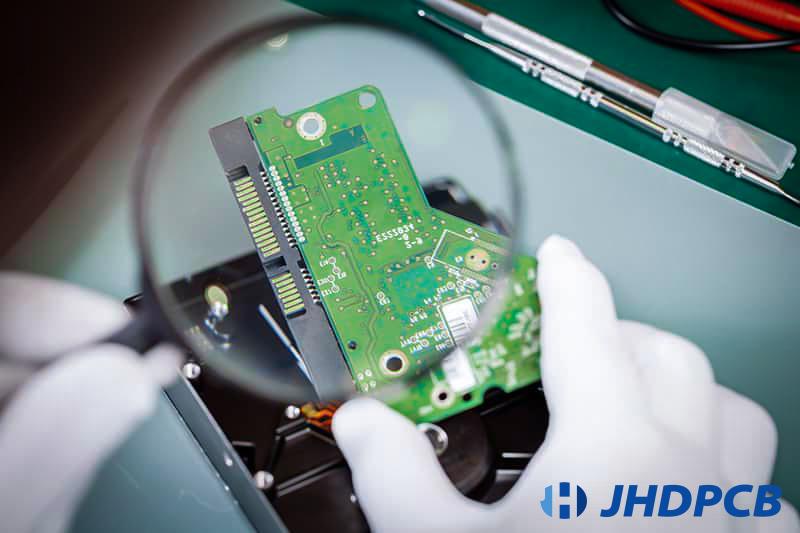
Visual inspection:
Visual inspection is part of the visual inspection, which is a manual manual test method that requires an experienced inspector to use a magnifying glass or microscope to check for weld defects and other visible defects with the naked eye. Visual inspection is suitable for visual inspection of circuit boards, seemingly poor solder mask application, component orientation or scratch smudges can all lead to circuit board failure.
Benefit:
Inexpensive and easy to operate – no test fixtures or complicated setup required;
Most major welding defects can be identified.
Shortcoming:
subject to human error. This may be decided by the skill of the technician;
Only visible solder joints can be inspected, hidden solder joints cannot be evaluated;
Time consuming, laborious, inconsistent.
Automatic Optical Inspection (AOI):
AOI inspection can reduce PCB bugs or defects on an beginning development step. AOI using a single (2D) or two (3D) camera to capture high-resolution images of the PCB board, and the program comparing these images to a detailed schematic or database of good or bad board images to find defects. AOI is often used as the first step in quality assurance. Make sure that problems are detected early and that production stops as soon as possible.
Different types of defects can be detected, and if the board does not match the schematic to some extent, the board is marked for inspection by a technician. Click to view detailed AOI inspection content.
Never depend only on AOI,automated optical inspection should be used in mixed with other tests. Some of the combinations that JHDPCB recommends to offer are:
AOI and flying probe;
AOI and online testing (ICT);
AOI and functional testing.
Benefit:
Most major welding defects can be identified.
More truly and precisely than manual visual inspection.
Applying in production line for defects detection at early stage .
Shortcoming:
AOI is a passive testing method – only surface defects can be detected.
Limited line-of-sight control to detect connections hidden by BGA or other parts.
100% coverage of all part types is not possible.
The setup and programming of template matching is time-consuming and has to be re-done for every design change.
Database matching may not be as accurate and reply on the quality of the database.
Online Test (ICT):
PCBA ICT is currently the most powerful and popular type of PCBA testing for high volume and mature products, and is a popular PCB testing method trusted by many PCB manufacturers and customers. Its fault extent to 95%. During PCB assembly ICT, electrical probes in the form of a nails bed send current through specific position on the board at designated testing points. These tests are used to verify the correct function, location, orientation and defects of each electronic component on the PCB. The test includes the verification of parameters such as short circuit, open circuit, resistance, capacitance, etc. The nails bed tester simply pushes the PCB board down onto the probe bed to start testing. Access points are pre-engineered on the circuit board to allow ICT test probes to connect to the circuit.
For high-volume or repeat batches, custom test fixtures can be made for faster and more efficient in-circuit testing. This test method is expensive, and the price will depend on factors such as board and fixture size. Therefore, it is strongly not recommended that you change your mind and move to an ICT strategy during production.
This testing way with special PCB testing procedures and equipment, including:
In-Circuit Tester: A tester system involve hundreds or thousands of arrays of drivers and sensors to perform test measurements.
Fixture: The fixture is connected to the in-circuit tester and is the component that directly interacts with the circuit board under test. This fixture seem like a nails bed and is designed for the particular circuit board.Every “nail” or sensor point is connected to the corresponding point on the PCB testing board, then feed back signal information to the in-Circuit tester.Fixtures are usually the most expensive part of the system.
Software: The software for the tester instructs the system which tests to perform on each type of board under test, and indicates pass or fail parameters.
Benefit:
The fault coverage rate can be as high as 98%;
Efficient and rapid testing methods for mass-produced products.
Shortcoming:
Test fixtures are an additional cost.
Not applicable to do low-quantity production or prototyping order, since any changes to the design file result in remaking the testing fixture.
Only test points are accessible, and the designer have to add testing points to the board.
Certain defects, such as too much or not enough solder, voids, cannot be evaluated.
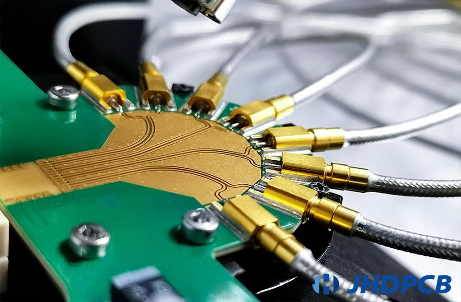
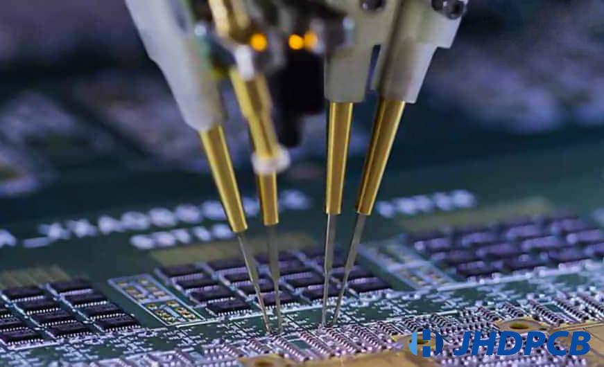
Flying Probe Test (FPT):
Similar in nature to traditional ICT work, flying probe testing is often seen as an improved version of bed of needles ICT. In addition to test points, the flying probe machine can access uncovered component itself just like test points, and can be programmed to check the values of passive components, directly check diode orientation and perform voltage measurements . Ability to adapt new boards quickly, cheaply and efficiently with simpler programming changes. This testing method makes it ideal for low-volume production testing and prototype testing, but is slow and not cost-effective for large-scale production.
The flying probe test is used to check:
Open, shorts, revolt, capacitance, impedance control, inductance, diode problems.
Benefit:
It is cheaper and faster to implement or modify. No fixtures required.
Wider testing coverage – Vias and component pads could be used as testing points.
Not required to add testing points. Save space.
Shortcoming:
Testing is too slow for large scale testing
Certain defects, such as too much or not enough solder, voids, cannot be evaluated.
Automated X-ray Inspection (AXI):
X-ray testing of the PCB is required when there are solder joints or pads for lead-free components that are not visible through a microscope or with the naked eye. X-rays can penetrate PCBs and component bodies, producing 2D or even 3D images of solder joints. This makes it ideal for inspecting hidden joints such as connections with solder joints under chip packages and ball grid array packages. AXI inspection can also test pseudo soldering, that different from many other optical inspection ways. While this inspection can be very useful, it requires a trained and experienced operator. JHD has specially skilled and trained staff to perform this operation, and you can deliver your PCB project to us with confidence.
When used with a production process, AXI can be used for early testing of defects, By makeing process adjustments to reduce the source of the problem. During this test, X-ray technicians were able to locate defects early in the manufacturing process by looking at:
Solder connection
Internal traces
Barrels
Benefit:
Can have the highest defect detection rate among common inspection methods;
Highlight long-life soldering joint quality, not only connections.
Shortcoming:
Requires trained and experienced operators;
Very time consuming and expensive process.
Burn-in (environmental) testing:
Burn-in testing is a more intensive type of PCB testing that can help you check performance and uncover hidden defects before your board is put into service. During the burn-in test, the burn-in test may cause damage to the component under test due to the test intensity. The circuit board is subjected to conditions exceeding the rated operating conditions to check out early faults and test the load capacity to clear up early faults in actual use. Power is pushed through other electronics, typically through the board at maximum rated current for 48 to 170 hours of continuous operation. Of course, not every PCB product needs to be subjected to burn-in testing, and it will only play its role in PCB projects with specific requirements and environments.
The operate conditions of the testing may involve in temperature, current, voltage, operating frequency or any other operating conditions related to the design. By collecting data in this process can help engineers better understand defects reason and optimize the design before manufacturing process.
Benefit:
Check performance under real-world conditions of use (something that other tests can’t achieve);
Better product reliability.
Shortcoming:
The testing process may shorten the life time of the product;
reduce overall production;
A time-consuming and labor-intensive process.
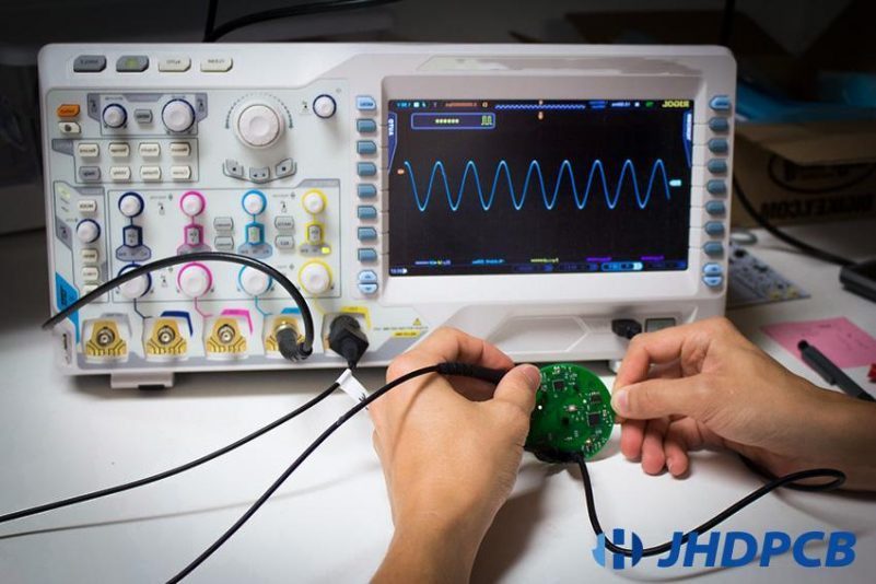
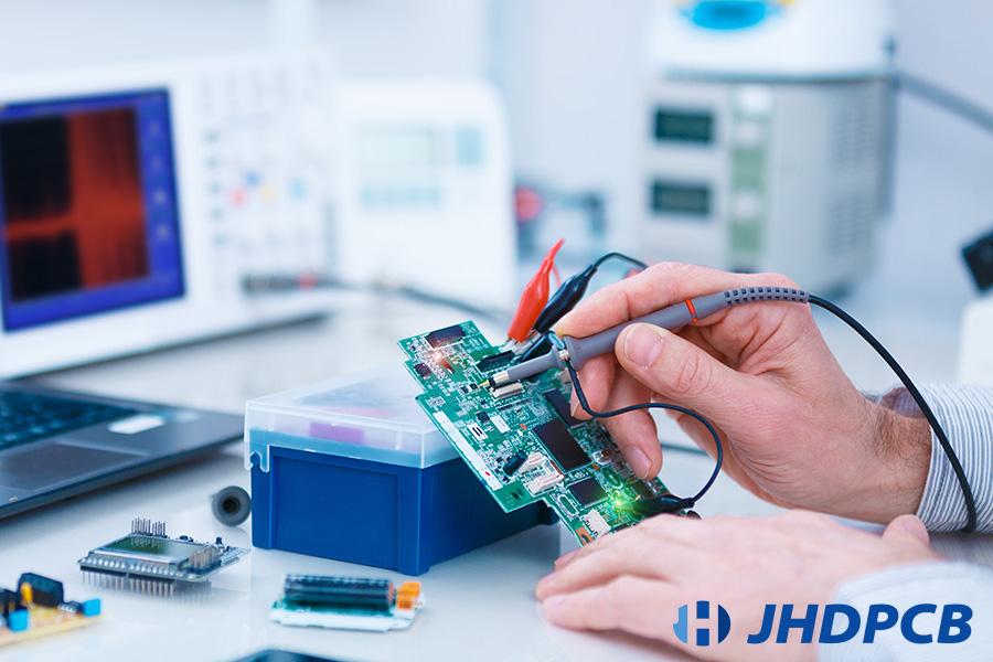
Functional Test (FCT):
Functional testing is the last step in the manufacturing process, and a functional tester is used to check whether the finished PCB functions properly. This doesn’t check out if the board is good, the presence of solder, or part tolerances. The circuits are properly powered and electrically excited through the interface connector, verifying their compliance with the design specification.
According to the complicacy of the design and the particular test requirements, the functional testing can be a simple switching power supply testing or a overall testing with strict protocols and test software. Because of its flexibility, functional testing can be used to replace more expensive testing procedures. Functional testing imitate the real operating environment and can therefore be more straightforward than other testing ways. Complete 100% functional testing is increasingly used in low-volume manufacturing to ensure that every board that comes off the production line is functioning properly.
Benefit:
Discover potential circuit anomalies;
measure the power absorption at a specific point in the circuit;
Flexible and highly customizable, almost all types of PCBs can be tested;
Lower cost and more convenient than other testing ways which need customized equipment.
Shortcoming:
The rate of defect detection reply on the inspections covered by the test plan;
The need for trained technicians to isolate the cause of the defect;
Under different stresses, the PCB boards may short circuit after passing the functional testing. Therefore, complex PCBs will also be tested with aging tests.
Boundary Scan Test:
Boundary-scan testing is a technique suitable for testing interconnections between components on a PCB. In this kind of testing, batteries are placed in leads from the silicon die to external pins to test the functionality of the board.
The biggest difference with this way of testing is able to detect the board without reaching all nodes. This quality is important for evaluating integrated circuits with multiple layers and high densities, as these types of PCBs have become more common in recent years.
In fact, this test method is so versatile that it can be used for a variety of applications, including functions such as system-level testing, memory testing, flash programming, and central processing unit (CPU) emulation. It is often used in field service to detect problems in functional systems.