Edge plating can also be called as Metalized edge plating, border plated, plated contour, side plating and castellation in PCB industry. The electroplating coating ranges from the top surface to the bottom surface of the PCB board and is the encapsulation of the edge of the PCB board. Plating can be performed on single-axis or multi-axis edges of PCBs. Often used to improve EMI shielding for high-frequency designs, and to improve chassis grounding for signals. According to IPC standards, When it comes to the definition of edge plating, there not exist an expressly stated definition. But it is generally accepted as a process of being plated with metalized materials. Electroplating materials are not only copper, there are many other kinds of materials used for PCB plating, such as gold, silver, tin and nickel.
PCB edge plating is also divided into three different types:
- Regular plane edge plating;
- Wrapping edge plating;
- Tooth edge plating.
Specialized equipment and professional and well-trained staff members are necessary for Printed Circuit Boards edge plating. The interior power planes coming to the edge of the circuit boards and the short circuit of edge plating would be caused by the nonobservance of working procedures. Edge plating is a method of enabling secure and strong connection realized in the Printed Circuit Board, also a remedy used to cut down the chance of costly board failures. In addition to this, edge plating can ameliorate chassis ground in systems and also refine Electromagnetic Interference shielding of high frequency designs.
For multiple axis boards, same as single-axis boards, edge plating is required to be implemented for all four edges. When the rout path is realized before the circuitry features of the PCB are metalized, there will exist edge plating. And sometimes, it also be described as “plated rout”.The size of every boards, the magnitude of edges of the boards, and whether the boards will be delivered in a multi-up array will be the design core of carrying out this technology. For the routing requirements, stability of the materials, which are used in fabricating the printed circuit boards, also plays a vital role in it. In order to ameliorate the structure of panel interior parts used to carry the parts during the process of manufacturing, not being the standard glass-reinforced FR-4 type materials may need an alternative routing design. An array, referred to the intact parts after being processed inside the carrier panel, is used for assembly and manufacturing. And under some circumstances, it requires the development of tabs for edge plating. Tabs might not be asked for stability for a single edge which needs edge plating.
At the present time, PCB Electroplating technology has been widely applied in many different industries, particularly applied in industries which require strong and secure connections.
The improvement of the reliability and the quality of Printed Circuit Boards (PCB) can be realized by improving delivered current conduction in circuit boards. If they want the components to be capable of operating like their design, the right level of conduction is indispensable. It can also prevent the more frail PCB edge connections from damage. Here’s what you can get to help when edge plating your PCBs.
Benefit one: Thermal Distribution.
The most prominent benefit of edge plating is that it can support thermal dissipation. Particularly when signal speeds increase, the circuit board will produce a great deal of heat, which is generally conducted to the interior ground plane and then evenly distribute all over the board by thermal vias. Because of the connection between the edge plating and the ground plane , it’s easy for the heat to distribute outside the board by the metal edge. At the same time, if the components is overheated, they may fail and have the possibility of leading to vitally potential damage to the printed circuit boards. In the wake of customer’s requirements of multi-functioned printed circuit boards (PCB), it’s inevitable to closely pack more components onto small circuit boards. Effective dissipation become the top priority, which can conduct overmuch heat going away from temperature-sensitive components. Too much heat will impact the reliability and performance of the printed circuit boards.
Benefit two: Signal and power integrity.
PCB edge plating can boost signal and power integrity. As the development of PCB boards becoming complicated, signal integrity needing more complex layouts and faster connection becomes a new requirement. For the equipment required, PCB edge plating can be seen as a straightforward process, but the order of the operating process might be different. The power and signal integrity of the PCB boards can also be boosted by reducing the level of electromagnetic interference. The improvement of current-carrying capabilities and the extra shielding of high-speed circuitry can be achieved by the extended grounding, which is provided by the PCB edge plating.
Benefit three: Electromagnetic compatibility.
Electromagnetic interference(EMI) can be generated at multi-layered circuit boards by the current, which is carried by the power and ground planes. This interference can cause radiation outside the system, and also lead to circuit boards exceeding the EMC standards that need to be met. Encapsulating the PCB board’s edges in the way of metal plating is an effective method of preventing electromagnetic interference form radiating.
Benefit four: Structural integrity.
Adding extra metal on the sides of PCB boards, which strengthens its rigidity and strength, can reduce the possibility of suffering physical damage because of being frequently used. The better support that offers the condition of sliding into the metal casing and frames of electronic system can be provided by the metal sides of PCB boards. During its use and handling process of PCB, accidental physical damages can be avoided by the way of edge plating.
Until now, metallization and non-metallization are two main ways to design PCB board edge. As the increasing development of technology, more and more customers choose PCB metal edge as their primary choice. As a result, the quality of metal edge that can cause a direct impact the use of products becomes the central issue for customers and manufacturers.
Next, let’s figure out the process of metalized edge plating.
- Drilling -> Milling metal slots -> Removing dirt -> Electroless copper plating.
Before the process of through-hole plating, the outer contour that will be metalized must be milled. Because during this manufacturing procedure, there exists the metalization of the edges. The anticipative surface finish is eventually applied to the PCB board edges after the procedure of depositing copper. The surface ENIG is strongly recommended by us.

Beyond that, let’s know something about the technical features of gold plating, which refers to the process of plating with gold and electroplating the side walls of the PCB boards with nickel and gold. Its features include as follow:
- Because of etching, the etching groove extending along the pattern to be coated with gold on the side walls, can be formed on the copper surface of the PCB boards. Then the copper layer requiring to be coated with gold is exposed.
- A dry film is pasted on the copper layer, and at the same time creates an opening. The opening is equivalent to the area of the etching groove and copper plate, which requires to be covered with gold.
- The PCB circuit boards are electroplated with gold and nickel so that the layer of gold and nickel and gold is plated on the area of the copper plate and side walls.
- During the process of plating the PCB circuit boards with gold and electroplating with nickel and gold, the distance length that starts from the circumferential edge of the opening to the circumferential edge of the copper plate is 4 mils.
In addition to the above content, we need to know the precise handling of the boards is the basic requirement for edge plating. In the meantime, manufacturers confront with some challenges that mainly focus on creating a lifetime adhesion for the plated materials and preparing the edges to be plated. The process of fabricating PCB circuit boards, this requires absolute control for it to limit latent damages in edge plating and PTH. The creation of burrs is the the most vital concern and we should pay attention to it. Because it can limit a lifetime adhesion of the PCB edge plating and cause the discontinuities in PTH walls. JHD’s strict quality control system can minimize defective rate.
Design rules
Part one, design rules involving design rules for overlapping copper area, design rules for PCB plating edges and design rules for the thickness of PCB edge plating.
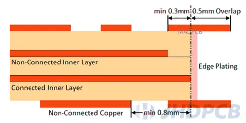
(1) Design rules for the overlapping copper area.
The overlapping copper must be used to define the metalized area in the layout file in order to make sure the fabricability of the PCB edge plating. About this aspect, we have three main points we should know combined with Figure below.
- The overlapping length is at least 0.50mm;
- The connected copper must be defined in at least 0.30mm on the connection layer;
- The minimum number of gap between the copper and the outer contour is 0.80mm on non-connected layers.
(2) Design rules for PCB plating edge.
It is required that the surface and the edges of the panel all should be encapsulated by edge plating. As you can see in the image below, the minimum length required to cover the surface is 0.015”. For the adhesion of the edge to the plating and interior processing, a wrap-around is needed. The wrap-around is required for internal processing and adhesion of the plating to the edge. In addition to this, from image below, you can tell the minimum length of a feature being placed to the wrap around plating is 0.010”. And also, for an adjacent routed feature, the required length is 0.010”.
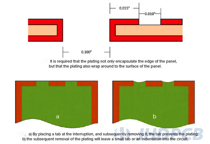
In normal cases, the plating along the total edge of the PCB circuit board is continuous. But the plating can be interrupted with two means.
- You can place a tab on the break and then erase it. The function of the tab is to prevent the process of plating. The first mean can be used under the condition that the minimum plating interruption is 0.200”.
- Plating can also be interrupted at the final wiring stage. A small indentation or a tab on the PCB circuit can be leaved due to the later removal of the plating. The second method can be used when the minimum plating interruption is less than 0.200”.
(3) Design rules for the thickness of PCB edge plating.
The first important thing we have to know is that the accepted and typical thickness values of PCB plating is around 100 micro-inches. The minimum thickness value for OSP and immersion silver can be 10 micro-inches. In addition to this, there exists two reasons for the significance of the thickness of plating materials.
The first reason is that the minimum plating thickness of every single IPC product class have been specified by IPC-2221A standard. Your products can meet any standards of IPC product classes, only when your plating thickness meets their specifications.
The second reason is that its losses can be affected by the thickness value of PCB plating. Under low frequencies, its losses cannot be affected by the thickness, such as under sub-GHz radios and low-speed digital signals. The loss problem occurs at mmWave frequencies, such as 24 GHz and higher. Under this situation, its losses are obviously affected and increased by the copper roughness. The extent of roughness when the signal propagates can be determined by the plating thickness. And the plating thickness can be revealed in the skin effect resistance.
Surface Treatment Panel Design Requirements.
- The orientation of the long side of the edging slot must run parallel to the direction of the long side of the rear panel (the running orientation of the tin spray is parallel with the orientation of the edging slot).
- If the manufacturer receives orders that do not meet the requirements mentioned above, the customers will be suggested and required to use non-sprayed surface processes, such as copper-nickel plating or gold.
Other matters needing attention
- The signal transmission or the customer soldering can be affected by the large position of the antenna on the gold pad.
- The short circuit can result from the connection between the wires on the boards and the inner edge pad.
- The handling of the stamp, at the edging groove, must be completed at the second process of drilling.
- It’s impossible to achieve a continuous metalization of the outer edges when the individual PCBs are manufactured as a panel through process-related fabrication. In addition to this, metalization can also not be applied in the small panel bridges.
- It’s required that solder mask can cover the side plating metalization.
Sometimes, wrapping the plating around the PCB edge is expected to form a connection rather than through a standard via hole. Because in this way, the edge can act as a conductor. The process of the wrapped plate can be accomplished by doing an extra main routing operation, which happens directly after the manufacturer finishes the drilling process. The exposure of the PCB sidewalls is the function of this routing step. This step can also enable it coated with a layer of electroless base copper in the same way as drilling holes being coated.
After the application and the development of the photographic circuit image, a conductive surface can be offered by the electroless layer. The conductive surface can allow more durable and thicker electrolytic copper on it. The routed region can be defined as a plated feature when a pad and other shapes can be included in the artwork. The routed channel sill be coated with electrolytic copper in order to create the required connection. It’s not too hard to get a great end, even under the condition that some steps are added to this process and the design intricacy of machining processes and array setups.
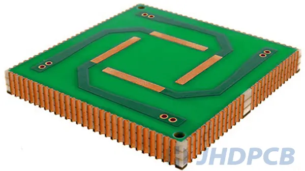
Tooth edge plating can be called castellated edge plating, which refers to plating a variety of drilled holes and making their center points along the PCB outline. The space of plated half-holes between them was left after when these holes are routed through. The installation of the pre-assembled components to either a region of a greater board or a small breakout board was generally facilitated by castellations. The method of the half-holes being spaced on the castellated board is often used to achieve alignment with surface mount pads on the greater board.
Under the condition of two boards being connected, the excessive mating soldering surface was offered by each half holes barrel plating. For the purpose of forming a more secure joint than a basic butt joint, the half-hole’s barrel will be wicked up by the assembly solder.