Production-related requirements of PCB manufacturing or several technologies require via protection, so the via fill can be very important to your PCB. In general, these types of via coverage are possible:
- Simple Coverage: Via Tent or Tent Vias
- Partial Fill: Via Plugging or Plugged Vias
- Fully Filled: Via Filling or Filled Vias
But sometimes designers don’t fully understand all the available via coverage types and which ones to specify. Rather than confuse designers and manufacturers by simply specifying that vias must be “plugged” or “filled,” we recommend specifying specific IPC-4761 via type. This helps to make it easier for designers and manufacturers to understand. IPC-4761 specifies only mechanically drilled via types, not laser-drilled micro vias. Learn more about the types of PCB through holes.
Here are seven different types of via coverages as summarized in reference to IPC-4761 “Design Guidelines for Protection of Printed Board Via Structures”:
| The well-known and reliable CCL(Copper Clad Laminate)manufacturer we are cooperating | |
|---|---|
| Type & Description | Via Covering Material |
I-a Tented Via (one-sided) I-b Tented Via (double-sided) 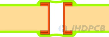 | Dry film solder mask |
| II-a Tented & Covered Vias (one-sided)  II-b Tented & Covered Vias (double-sided) 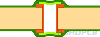 | Dry film solder mask + LPI solder mask |
III-a Plugged Via (one-sided) III-b Plugged Via (double-sided)  | Plugging Epoxy (non-conductive paste) |
| IV-a Plugged & Covered Via (one-sided)  IV-b Plugged & Covered Via (double-sided)  | Plugging Epoxy + LPI solder mask |
V Filled Via | Plugging Epoxy (non-conductive paste) |
| VI-a Filled & Covered Via (one-sided)  VI-b Filled & Covered Via (double-sided)  | Plugging Epoxy + LPI solder mask |
VII Filled & Capped Via | Special Plugging Epoxy + Copper Plating to planarization |
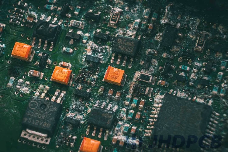
Via tented refers to covering the vias and annular rings with solder mask, that is, creating a shape like tent over the opening to hide the vias. A via is a hole comes from a PCB that allows signals connect from one layer to another on the PCB. Vias are generally copper-plated, so this material is strongly conductive. The main purpose of tenting vias is to reduce the number of exposed conductive pads on the PCB and decrease unexpected short circuit or touch circuits. So far, tented via is the most developed and prevalent process in PCB manufacture. Via tenting means that the through hole is only covered by solder mask ink . This is the easiest way of Via Covering. No additional process steps are required in the manufacturing process. Generally, vias using this type of coverage should not be larger than 0.3mm.

The main role of the tenting vias is to reduce the exposed conductive pads on the surface of the PCB. Exposed conductive pads can cause the migration of solder during handling, which mostly occurs when vias are located at the edge of the SMT pad. A via tenting not only reduce the solder paste migration on SMT pads, but also help cut off oxygen and moisture from the environment and avoid vias from being damaged by exposure to the nature.
When building PCB tented vias, the diameter of the vias is required to be small. The diameter of the via hole is less than 12mil, and the tent will be more effective. For vias over than 12mil in diameter, it is recommended to consider using some kind of filler to seal the holes. Because the copper-plating on the vias is very conductive, you don’t have to worry about the conductivity of the material when filling the vias.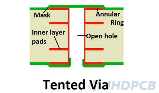
Advantages:
- Tented vias can prevent damage to the PCB layer. the Solder mask to cover vias can protect copper traces from corrosion and oxidation
- Tented vias can reduce the number of conductive elements exposed to external element. In case of the inside of the via is prolonged exposure to the outside environment, it will cause corrosion of copper.
- Tented vias is an economical and effective protection method. Masking vias with liquid photoimaging solder mask is the most cost-effective way of masking.
Disadvantages:
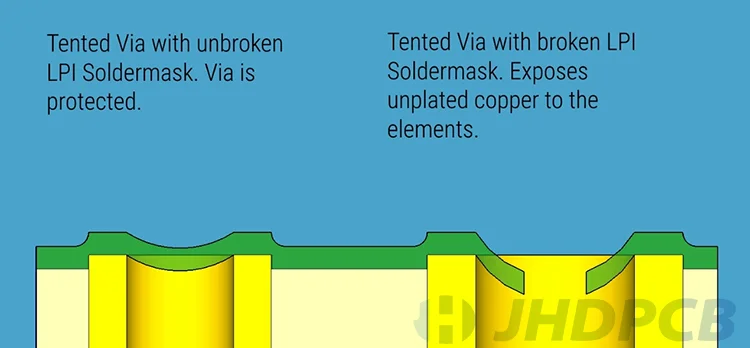
- An obvious disadvantage of vias tenting is that because the solder mask used is a liquid, the liquid may crack after drying, and making small holes in the tent. The small holes that create can absorb chemicals and moisture, which can cause corrosion. In this way, the copper plating inside the barrel will also be gradually eroded, it will increase the possibility of via failure.
The solution to this problem is to expose the vias when the PCB is in the prototype stage of the manufacturing process. This helps to identify problems and fix them in a timely manner.
When building vias tent, there are some points we need to pay attention to. The followings are explanations about close to SMT, assembly, and selection of double-sided.
Close to SMD:
If the via is placed too close to the SMD, it may cause the solder wick to stick to the back of the board. Here are three methods with the potential to prevent solder wicking:
- Selectively cover any vias near the SMD pad without altering the paste mask.
- Reduced solder paste mask opening so that less solder paste is deposited on problematic SMD pads.
- Keep these vias away from the SMD pads and make sure there is some solder mask between any pads and their connecting vias.
Assembly issues:
Sometimes tented vias can create some assembly issues. The following two issues you should consider when assembling tented vias for your PCB.
- Cover the vias near the component package if there is a chance of solder being drawn to the back of the board during assembly.
- Eliminate vias near or below the component package if excess flux residue will cause contamination and possible shorting issues. Learn more about PCB package process information.
Two sides:
Should the tent punch holes be on one side or both sides? Doing it on both sides of the PCB is the most ideal way. If only one side is tented, the un-tented vias on the other side will be exposed to the outside, leading to corrosion and oxidation. Especially in the double-sided PCB manufacturing process, it needs to be paid attention to.
Plugged vias refer to a PCB technology that completely fills the hole with epoxy resin or closes the hole with a solder mask. There may also be no solder mask. We can think of the plugged via as a protective measure, which prevents excess solder material from flowing during soldering or assembly. Conversely, if a via is not plugged during soldering, solder will flow from the pad down the vias and may create unnecessary solder joints. The diameter of the plug hole is required to be less than 0.5mm, and the via hole can also be filled on both sides or on one side.
Today, BGA packages with smaller pitches or clearances are becoming more and more popular. Signals transmit from the BGA pads to the vias, and from the vias to other layers, instead of using standard “dog-bone” footprint, the vias can be drilled immediately into the BGA pads.
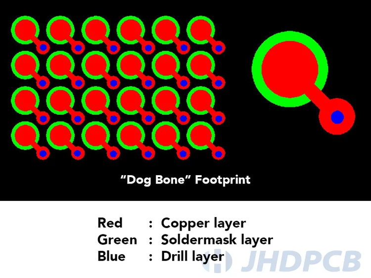
In this way, the track routing become easier and tighter when designing a PCB, as the via surface itself becomes a BGA pad, which can be soldered as if it were a normal SMD pad. This process is called “Via In Pad” and the pad is called “Active Pad”. More PCB pad knowledge can be learned through our blog.

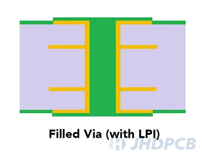
Via filling in PCB is a technique in which the via hole is filled with epoxy. This process completely or selectively uses conductive or non-conductive epoxy as the filler material to fill vias with epoxy. Filled vias provide better assembly yields, more reliable surface mounts, and improve the reliability of PCB by reducing the possibility of trapped liquid or air in the PCB board and in the vias.
Conductive via fill enhances the thermal transfer characteristics of the vias because it allows electrical signals to be efficiently transmitted from one side of the board to the other. Conductive filled vias are very helpful in conducting a large amount of heat away from the component because the conductive vias are filled with silver and copper particles distributed throughout the epoxy to provide additional thermal and electrical conductivity.
When choosing conductive epoxy for filled vias PCB, the typical materials of choice are between the DuPont or CB100the silver-coated copper particle epoxy matrices of the Tatsuto AE3030 epoxy fill. Both of them are electrically and thermally conductive when cured.
Non-conductive via fill uses essentially the same process as conductive, but the purpose of this is not to conduct heat and signals, but to prevent solder or other contaminants from entering the vias. In the case of a via-in-pad, it also provides supporting structure for the copper pad coating the hole. Note that non-conductive filled vias have copper planting vias to conduct heat and power as usual.
When choosing a non-conductive epoxy for PCB via fill, Peters PP2795 epoxy is usually chosen. The previous replacement was San-Ei Kagaku PHP-900 epoxy. Regardless, both should cover your basic needs when it comes to non-conductive via fill epoxies.
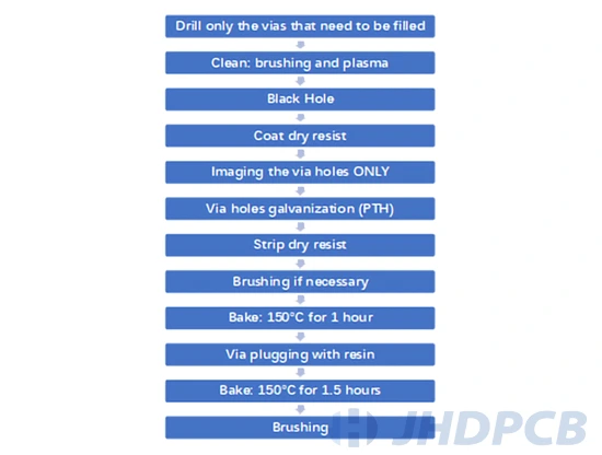
Via Filling with Resin: The vias to be filled are filled with a specific hole plugging resin, TAIYO THP-100 DX1 heat-curing enduring filler material, using a dedicated machine, ITC THP 30. The additional production steps required are performed prior to the 2-layer PCB production process. This will be after pressing if making multi-layers.
Outline of the additional processes:
IPC-4761 clearly defines the difference between filled vias and plugged vias through the classification of protection types.
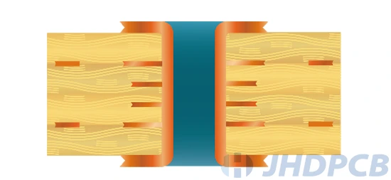
Filled vias
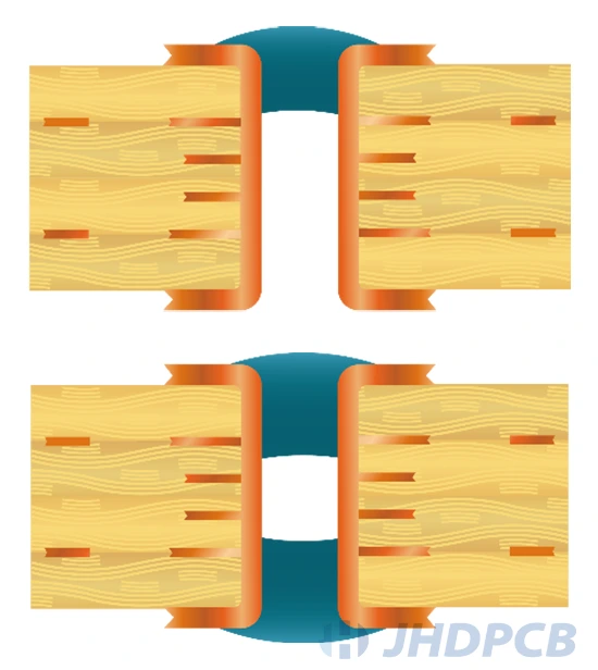
Plugged vias
The following shows some recommended and non-recommended types from the seven different types of via coverages:
| Recommended Via Types Protection | Not Recommended Via Types Protection |
|---|---|
IV-B Plugged & Covered Via V Filled Via VI-A Filled and Covered Via VI-B Filled and Covered Via VII Filled and Capped Via
|
III-A Plugged Via (Not Recommended Long-Term Reliability Risk) III-B Plugged Via IV-A Plugged and Covered Via |
Filled and plugged vias can enhance the PCB reliability by reducing the probability of air or liquid entrapment in vias, insuring finished product ratio through assembling. However, as can be seen from the above table, the PCB filled vias that have more advantages than plugged vias will be selected in our actual manufacturing process.


