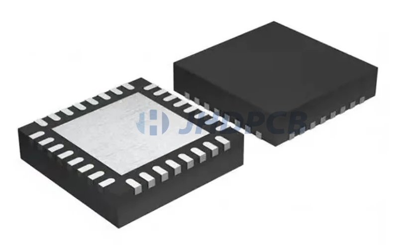
QFN is a leadless package, which is rectangular or rectangular. Similar to chip level package (CSP), it is processed by cutting machine. There is a large area of exposed pad at the center of the bottom of the package for heat dissipation. There is a conductive pad for electrical connection on the periphery of the package with the large pad. QFN packages do not have gull-wing leads like traditional SOIC and TSOP packages, therefore, the conductive paths between internal pins and pads is very short, and low inductance and supplier resistance of wiring resistance within the package, which can provide prominent electrical performance. Additionally, it offer excellent thermal performance through exposed leadframe pads with direct thermal paths for heat dissipation within the package,Typically, thermal pads are soldered directly on the board, and thermal vias in the PCB help spread excess power dissipation into the copper ground plane, which absorbs excess heat. Due to its small size and light weight, coupled with outstanding electrical and thermal properties, this package is ideal for any application where size, weight and performance are critical.
QFN is defined by the Japan Electronic Machinery Industry Association, which is the abbreviation of QuadFlatNo-lead Package in English; DFN (DualFlatNo-lead Package) package belongs to the extension package of QFN package. The pins of the DFN package are distributed on both sides of the package body and the overall appearance is rectangular, while the pins of the QFN package are distributed on the four sides of the package body and the overall appearance is square. View more PCB package types.
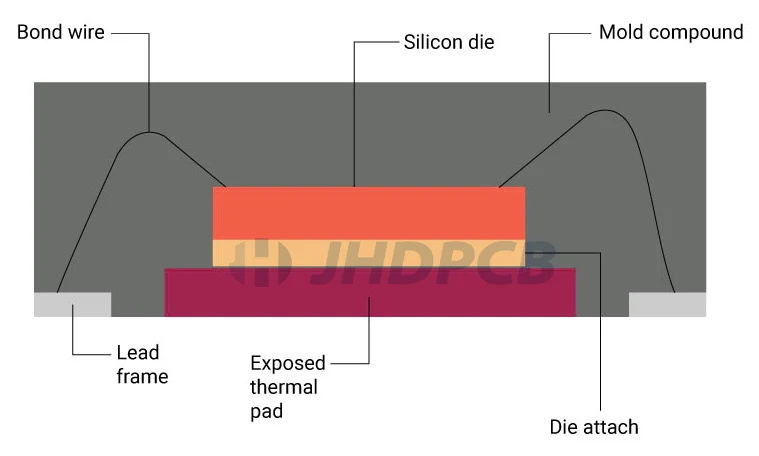
The QFN package has a die surrounded by a lead frame(Made of copper alloy with matt tin coating).
Chips and frames are usually connected to each other by wire bonding. Copper/gold is the first choice for wire bonding.
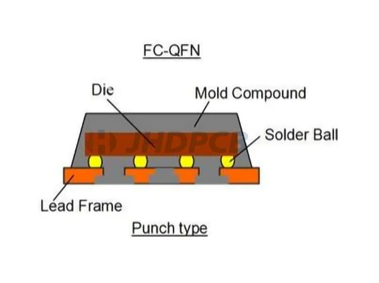
Flip chip technology is used by some manufacturers for this interconnection. Compared with traditional technology, flip chip technology provides better electrical performance. On the bottom are the metallized terminal pads,which exist along the four edges of the underside and provide electrical interconnection for the PCB.
Multi-Row QFN Package
Multi row QFN can perfectly solve the application technology that requires high number of pins. Multi row QFN provides multiple rows of pins, which is very similar to BGA technology, and in most cases also provides lower costs than the latter.
Fc-QFN Package (Flip-Chip Quad Flat No Lead)
This is a low-cost molded package that uses flip chip interconnects on a copper lead frame substrate. This package provides small form factor compared with conventional QFP packages. Due to the short electrical path, it also provides better electrical performance.
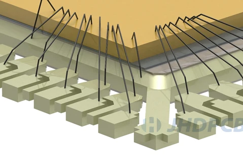
Wire Bonding
Wire bonding is generally considered to be the most cost-effective and flexible interconnection technology for assembling most semiconductor packages.
Pull-back QFN
The metal pad pulled back from the edge of the component body is unique to this packaging, and the terminal is invisible after installation.
QFN with wettable flanks
The QFN with the wettable side has a level that indicates solder wetting. This allows the designer or manufacturer to ensure that each pad is mounted on the circuit board and see the entire process.
open-molded plastic package
The Exclusive Open Molded Plastic Package (OmPP) is a preformed air cavity QFN package (Quad Flat No-Lead) that features your needs for IC packaging and IC high quality, fast solution assembly. These QFN packages or Open Molded Plastic Packages (OmPP) are available in a variety of sizes, especially for prototype, mid-volume or volume production applications.
Air Cavity Plastic (ACP) Package
This packaging structure is very similar to ACC, but the cover and ring frame are made of polymer rather than ceramic. This allows the ring frame to be bonded to the flange rather than brazed and reduces flange stress and deformation. In addition, thinner matching capacitors are allowed to reduce RF losses at the gate and drain.
Multi-Die QFN
It is used to package multiple chips on the same pcb board. It means that multiple chips are packaged in series on the same circuit. The technical difficulty of this type lies in the relatively complex control of circuit impedance and inductance.
QFN Marking Specification:
The QFN package is relatively small, so now there is really a lot of room for clear marking. A 5mm x 5mm QFN can have up to 5 or 6 characters in a line; 3 or 4 rows are possible.
QFN Issues:
As a PCB designer, you may know that QFN manufacturability is a key factor. Although QFN is very efficient, PCB designers often encounter problems. When encountering the need to reduce the failure rate of reflow and mounting, we often encounter some challenges. QFN performs well in large batch and low mix products. However, when they encounter small batches and high mixtures, things tend to get a little worse. What’s worse, this problem seems to affect two main aspects: * steel mesh design * circuit board design. Therefore, when dealing with steel mesh design, you must have accurate steel mesh thickness and aperture design. If these two are not accurate, the result will be disastrous.
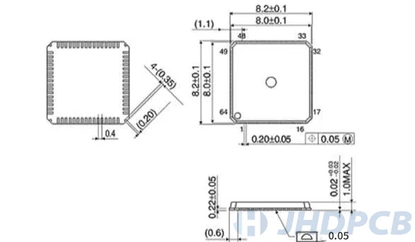
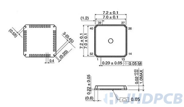
QFN footprint design:
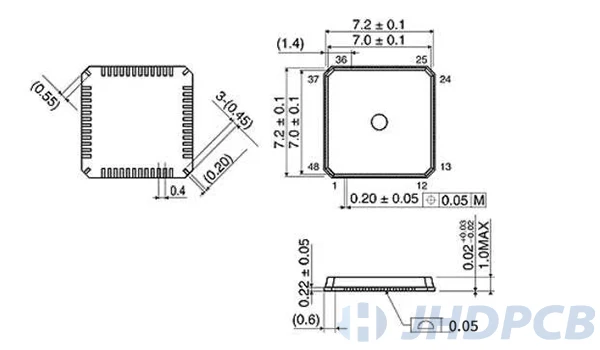
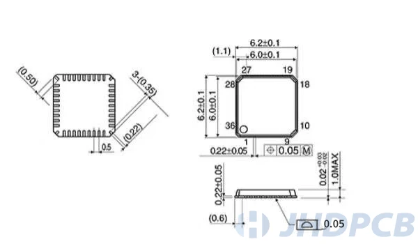
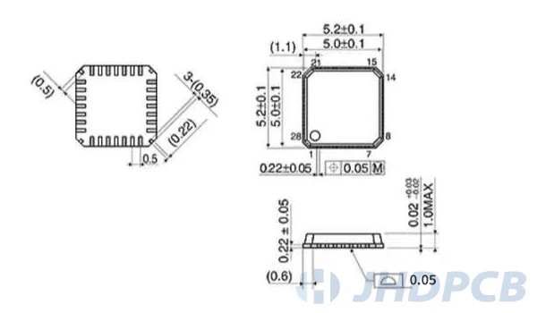
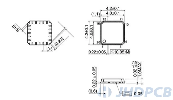
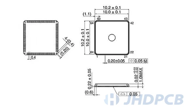
When designing encapsulation for QFN, please read the component data sheet carefully. The data sheet will contain footprint drawings. This figure forms the basis of packaging design. The detailed package is shown in the following figure:
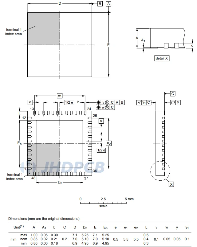
The following must be noted when designing the footprint of the QFN package:
- Orientation marking/Pin 1 marking.
- Ground pads (EP pads) should have a sufficient number of vias for heat dissipation.
- Check the solder mask and solder paste layers. Leave the opening as recommended by the manufacturer.
- Solder mask bridge should be 4mil or larger.
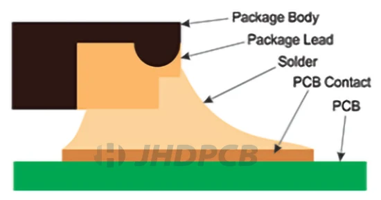
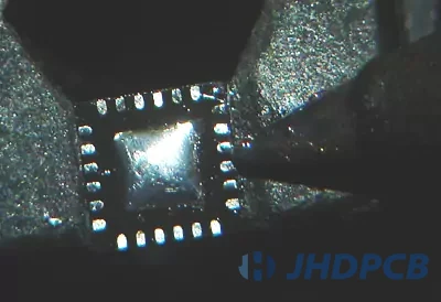
First of all , the original chip is removed by preheating the board and applying hot air using the same method detailed below. The removed chips and pads on the board are then cleaned by adding flux and using solder wicks.
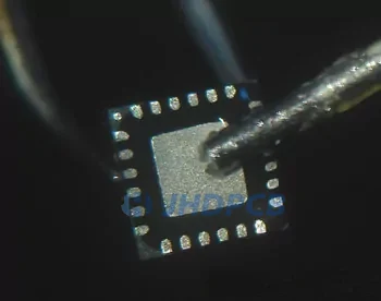
Cleaned QFN pads – note vias in heatsink pads.
The radiator has several through holes (applicable to the small holes on different layers of the connecting plate) to help remove heat from the components and enter the ground plane. Even though these help keep the chip cool during use, they make soldering difficult, and the heat from the hot air tool will quickly dissipate to the integrated circuit board. Preheaters are particularly useful if you are welding intermediate radiators. However, it is not necessary to weld this intermediate heat sink in many cases, which is why welding this chip is particularly challenging. Therefore, if you do not need it, do not add solder to it. If this is your first time welding QFN, it is better to skip this step.
When you add flux to the bottom of the clean QFN chip, remove any old flux residue with alcohol and brush at first , and then apply new flux.
Apply solder to the radiator in the middle: To get a very small solder pillow, you need to tap a very slight tin tip on the pad until the solder core is absorbed. You can check the pillow height after measuring the thickness with a caliper. Too much solder on the pad can cause a short circuit. Remove the superfluous material by applying flux and touching the pad with a clean tip.
You should tap a very slight tinned tip onto the pad until a small amount of solder core is absorbed. After this step, the solder pillow should be very small, and its height should not exceed one thousandth of an inch (1/3 inch). If you have a caliper, you can check the pillow height by first measuring the original thickness and then comparing the welding thickness. If there is too much solder on this pad, it will be short circuited to the external connection during reflow. Better not too little. Remove excess material by applying flux and touching the pad with a clean tip.
Then put the device on it (pay attention to check the correspondence between the 1-pin of the device and the package), gently press the surface of the device twice with tweezers, and finally fix the edge of the device with a soldering iron. two pins. Once the device is secured, then touch the perimeter connections with a lightly tinned iron tip. There should be small solder beads on each pad. A microscope or magnifying glass can be used to ensure that each pad accepts solder. Check that the device and pads are aligned. If there are no problems, it’s time to start soldering the other pins; if there are device bias pins, you’ll need to adjust the position of the device. Do not start soldering until the corresponding pins are soldered, otherwise it will be difficult to adjust the position of the device after soldering all pins.
The soldering process flow looks very simple, but it is difficult to operate in practice, because the soldering of QFN packages is prone to false soldering and tin connection. Therefore, you can send solder several times during the soldering process flow. Remember before sending solder Apply solder paste, which can effectively prevent virtual soldering and tin connection.
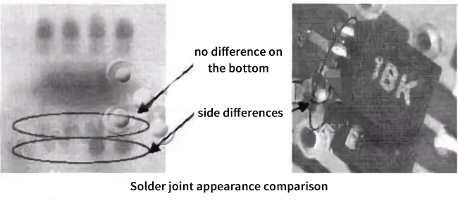
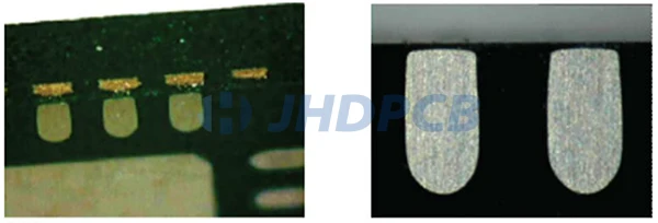
Because the solder joint of QFN is under the package, the thickness is relatively thin. Therefore, X-ray cannot detect open QFN solder joints with less tin, and can only rely on external solder joints.Judgment, but the current judgment criteria for defects on the side of QFN solder joints have not yet appeared in the IPC standard. In the absence of a better method for the time being, we will try our best to rely on the test station in the post production stage to determine whether the welding quality is up to standard.
As can be seen from the X-ray image below, it can be seen that the difference in the side part is obvious, but the image of the bottom part that really affects the performance of the solder joint is the same, so this brings a problem to the X-ray detection judgment. Adding tin with an electric soldering iron only adds to the side part, but X-ray still can’t judge how much it affects the bottom part. As far as the enlarged photo of the appearance of the solder joint is concerned, there is still a clear fill in the side part. Click to see more PCB inspection methods.
For mass production, sawing QFN is preferred, while stamping type is usually used for small batch products. The similarity lies in the electrical and thermal characteristics.
The following figure demonstrates the differences between the packaging structure of stamping and sawing QFN.
ntation method,in which you can separate the stamped qfn using a stamping tool and the sawed QFN can packaged into a single unit by sawing in bulk.

QFN can be divided into die stamping type and cutting type. The two types of summaries are as follows:
- ANVIL singulation:
This is a qfn package, which is characterized by stamping and cutting the outer lead wire with a die. Because of the resin sealing of each cavity, the peripheral pins of the package are stamped with a die. Since the pressure is cut off, there is a very short protruding xd pin on the periphery of the package. - SAW singulation:
This is a QFN package that uses a rotary blade for cutting. Since the package sealed in the same cavity is cut off by a rotary blade, the package end face (side) same as the pin end face side.
With the rapid development of modern electronic information technology, electronic products are developing more and more in the direction of miniaturization, portability and multi-function. Electronic packaging materials and technologies enable electronic devices to eventually become functional products. A variety of new packaging materials, technologies and processes have been developed. Electronic packaging is promoting the development of the information society together with electronic design and manufacturing.
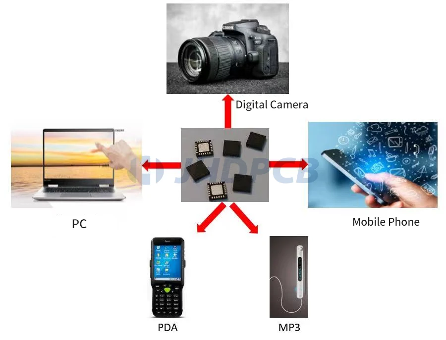
The small form factor of the QFN package can be used in portable consumer electronics such as:
- Laptops,
- digital cameras,
- personal digital assistants (PDAs),
- mobile phones,
- MP3 players.
In addition, other package types derived from traditional QFN can also design more pins and have certain secondary wiring functions, and also have certain development potential. QFN package is a highly applicable, simple and cost-effective package.
The terminal pads of the QFN vary according to design, shape and size. The following are a variety of terminal pads available.
Fully exposed terminal ends:
The terminals are completely exposed at the package edge and package side in this type.
Pull-back terminal ends:
Both ends of the terminal are pulled back from the edge of the package. For this type of terminal package, it’s unnecessary to add solder fillets after reflow soldering.
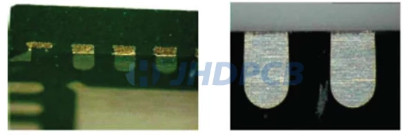
Side wettable flank terminal ends:
These types of terminals are a variation of totally bared terminals. The side can wet the side terminal to wet the solder to form a solder fillet. If a uniform solder fillet is formed, it will be easier to use AOI for solder fault detection. This saves the step of X-ray inspection.
In order to provide you with better products, JHDPCB company is very strict in the assembly of qfn package and its quality process control.


