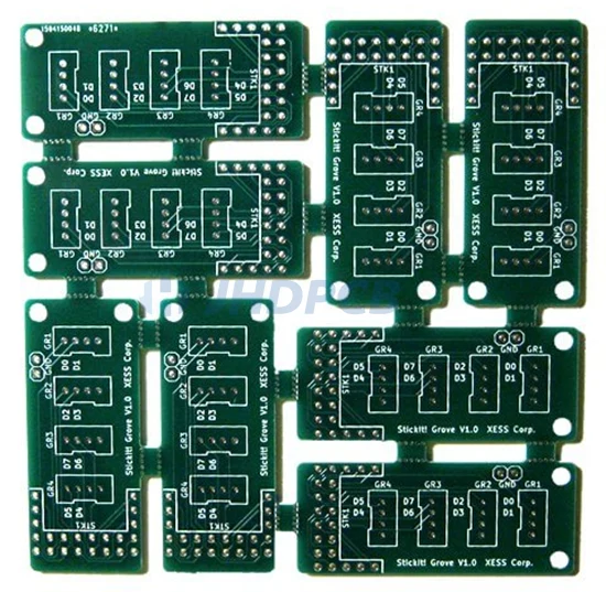
PCB panel, also known as PCB array. Considering the efficiency of PCB manufacturing, panelization is essential. Aggregating multiple PCBs for fabrication on one large board is known as panel creation. PCB panelization is a fabrication technique which makes it easy to pass through the assembly line owing to the fact that the smaller PCBs are fabricated as a single array by being integrally connected together. And it’s so easy to separate or remove each board from the array so that packaging or installation in products. Alternatively increasing the width to accommodate the assembly line by a PCB processing edge around an individual PCB. Panels are typically applied to high volume PCB production. PCB panelization not only improve total output , but also allows designers to change dimensional to improve overall pcb panel utilization and save costs. There are always different board types to choose from during the PCB order placement process: single board design or panel design. Because some boards are irregular, the panels can reduce the time cost and labor for production and testing. Additional planning is required if the PCB is too large for the panel or if there are other special requirements.
We will help you connect single boards (same or different) to large panels through different wiring processes, the reserved micro gong slots can easily break them down into a single PCB when you need them. The routing process is often divided into three types: V-scoring, Tab routing, and punching.

To panelize pcb not only helps smaller boards to adapt to standard production procedure, but also increases production efficiency. And there are some advantages of PCB panelization, including:
- Save time & money:
PCB control panel enables you to spend less money and time owing to mass production. Building many boards in a large panel is more cost-effective than building them individually. Meanwhile, it can also save the time, money and labor. - Improves Work Efficiency:
As a means to improve PCB productivity, it is a common practice to install multiple smaller copies of the printed circuit board in the fabrication of panel. It is an effective way to fabricate and assemble the boards rather than manufacture them one by one.
The identical material and stack-up configuration must being included in panels as the printed board. The important thing is to choose the panel size (whether small or large) which best fits your needs of printed circuit board, various manufacturing and assembly processing. If you can fit more boards into PCB panel, the more efficient of the manufacturing you will own.It will also reduce waste of panel space. - Improve Produce Quality:
PCB paneling is not an optional fabrication process, because you will need to panelize them if you produce large quantities of similar circuit boards. Due to the goal of panelization is to board uniformity, related components are placed on different boards at the same time, there will be less of fault occurring in the manufacturing when you use panelization. When you produce smaller circuit boards and need to ensure the components are similar and uniform, PCB panelization will occur. This process helps to guarantee the quality of the product. - Add Different Designs:
PCB designers can use panelization techniques to make different designs all once. The nature of panelizing a printed board is to copy the models to stuff the space of panel and reduce waste of materials. As a PCB designer, you can arrange the boards to utilize the areas of group to make prototype PCB boards with various designs. For example, you can panelize a small rectangular board and a large L shaped printed board in a single panel if they have matching layer and similar components stack up configuration. Learn more about PCB design layout. - Increases Output:
It can ensure that the manufacturing process of the PCB produces maximum output in a short time by panelization. It means that you can make a much smaller PCB without wasting time. Panelization allows you to make large quantities of PCB at the same time, while saving production cost and maintaining quality. - Product safety:
Panelization can offer protection from vibration and shock or mechanical stress for every individual printed circuit board. If you use laser depaneling, these damages can even be completely avoided.
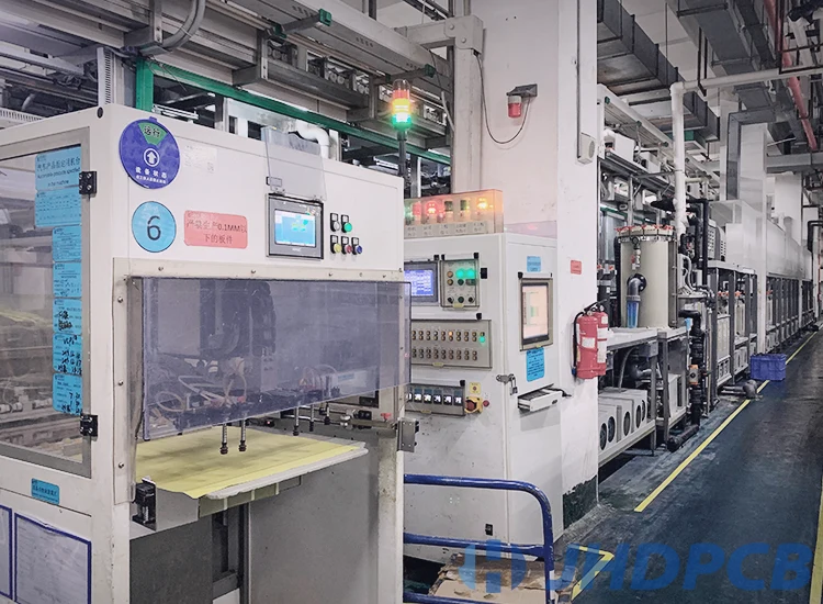
In the PCB design, it is also an important thing to assembe the PCB when the final PCB mass production is carried out. This process not only affects the cost of PCB production, but also include the quality standards of the PCB circuit board. It is an important problem that production companys pays great attention to how to produce effective and reasonable splicing with the premise of ensuring the quality of PCB circuit board.
There are many methods of panelization, each with its own advantages and disadvantages. It is the design of the boards on the panel and the panel itself that often play an important role in which panelization method best fits the application.
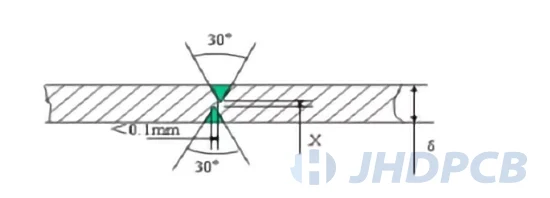
- V-Score Panelization: It is a common method of panalization to separate individual PCBs with V-shaped grooves. These grooves are made by cutting from the bottom and top of the board one third of the thickness of the board with an angled blade. Considering the remaining third of the board between the grooves is so strong that a machine is commonly used to the process of breakout, because hand-breakout will give stress on the PCB and components.
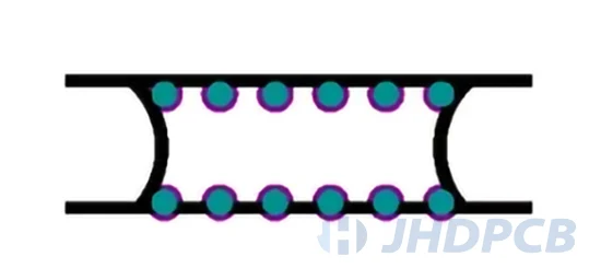
- Tab Routing Panelization: The method of V-groove will be instead by a tab routing method when it can not be used in PCB arrays. When you use this method, PCBs should be pre-cut from the array and be hold on the board with perforated tabs. Typically three or five holes are used in these perforation patterns. It is very easy that individual circuits can connect the panel frame through narrow which can be broken to remove the individual circuits boards. It is advantages for its designs of ability to support with edge-hanging components. It can also be broken through hand.
- Solid Tab Panelization: Some arrays are designed to improve the strength through solid tabs between each board. However, the method for this type of PCB panel needs either a laser-cutting machine, a hook-shaped blade tool or a depaneling router. The router may be cause vibration and dust, meanwhile the laser-cutter is very expensive and it will become inefficient on the boards of over 1mm thick. Although this holk-bladed option is cheaper, it is inefficient and the blade prone to rotation. Therefore this method is less common than others.
- Punch/die cutting: A fixture with die cutter is used to punch out individual boards from a panel. The blades and fixture must be customized for the board.
- Laser cut: Sometimes it is named laser router, and it is suitable for designs which are tight tolerances or unusual shapes. This process is fully automated, and it can be used to carve any shape including sharp corners and curves, and will not make any mechanical stress.
Although V-groove panelization is suitable for so many applications, it has limitations in PCB panel design. For example, V-groove panelization is not fit for those designs where components are placed too close or hang over an edge. And they also present various manufacturing problems which must be considered in the design process, such as:
Jump-scoring: V-grooves will reduce the structural integrity of a PCB array and lead to the leading and trailing edges to droop when it go thourgh the wave-solder machine. This will make the PCB array to warp and get caught in the wave-solder machine. In order to prevent these issues, designers can add jump scoring to the leading and trailing edges of array.
Tab Routing and V-Score are the preferred panelization approach for most applications. For PCB designers, the most important thing is to learn which one is best of two means for their application. And then, they should design their array for maximal strength and breakout success.
Many people prefer to use V-groove panelization as much as possible, because its high efficient and reduction in surface stress. It is relatively cheap and cost-efficient for this type of array to use of depaneling machines. Better yet, they require less maintenance and they are portable. Although this way may leads to rougher board edges, it is rarely a concern for applications of using of V-groove panelization. Therefore, V-cut is generally suitable for rectangular PCBs. The characters of it is low processing cost and neat edges after separation.
Tab route imposition is generally applicable to irregular imposition. For instance, the link way of stamp holes is often used for MID’s “L”-shaped frame structure for imposition.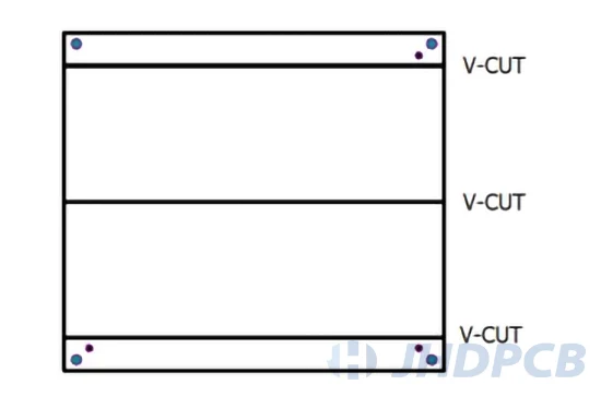
It is also called characteristic panelization. It is a process of combining different types of printed circuit boards according to the principle of combination. On the one hand, there are some good features in this process. This process is suitable for producing models with various types of printed circuit board combinations, such as household and some toys. It is so helpful that improve the efficiency of production and save the cost. Meanwhile, the turnover and semi-finished products of the product will not be piled up as inventory, and it is enough to meet the customer’s requirements for fast shipment. On the other hand, there are some disadvantages of it. On the printed circuit board assembly line, differentiation of products is hard to administrate, which eventually leads to process confusion. During the process of panelization, if one borad is of good quality and the other is versa, the sum of such panelization will be reduced and the efficiency of manufacturing will be bought down. The are two method of combination, they are:
Combination panelization (AAAA):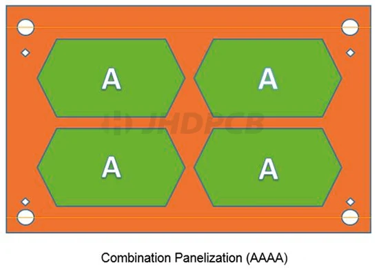
AAAA combination panelization is a commonly used panelization method, and it is the most widely used one. Many advantages have allowed it to achieve its current leading position. First of all, this kind of paneling is suitable for all situations, without considerations of the manufacturing conditions and product mix of SMT manufacturers. Second, order panelization is not affected by fabrication quantities, allowing the maximum panel quantity to be effectively based on the maximum quantity of SMT device, resulting in the highest manufacturability across all panel combinations. Third, during the process of printed stencil design, the qualith of printing would not be reduced owing to the influence of the orientation of special component pads. Finally, operational difficulty would not be accumulated due to the different orientations of panels each time they are run throughout the process.
Combination panelization (ABCD):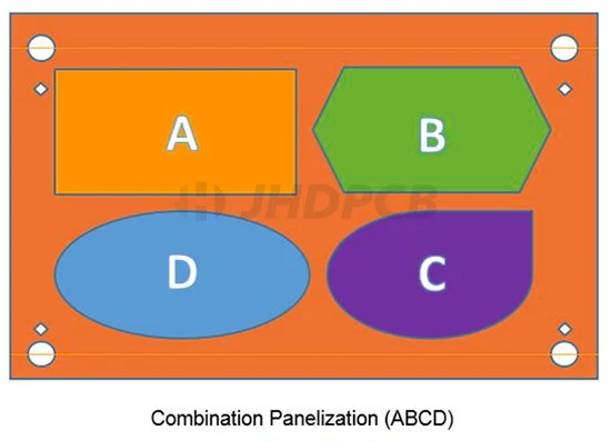
This kind of panellization owns some advantages. In the first place, it is suitable for the manufacturing mode that contains multiple PCB combinations in products such as toys and home appliances. In the second place, it is conducive to improving production efficiency and reducing costs, greatly reducing the product turnover rate and semi-finished product inventory, and can meet the requirements of customers for rapid shipment.
To optimize your process of production, we recommend the following key figures:
Rule 1: Veneer with Broken Edges
No large devices or protruding parts are allowed near the connection point between the outer frame and the inner board and the connection point of each inner board. If components are put on the outer edge of the PCB, they cannot be automatically transported in the production line. Therefore, the minimum distance from the outer edge must be ≥ 3mm for SMD components and at least ≥ 5mm for THT components. If this is not possible, a breaking edge (or panel) must be defined.
Rule 2: Scoring Teams
The printed circuit board in the scored panel is placed without spacing. Due to tolerances when singulating individual PCBs, all conductor and copper areas should be ≥ 0.5mm from the scored edge.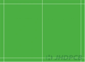
Rule 3: Milled-scored panel
Please note that the distance between the scribing circuit board must be counted as 0.0 mm. A distance of 2.0 mm should be planned between boards. All lead and copper areas shall be ≥ 0.5 mm from the edge of the score and ≥ 0.2 mm from the milled edge.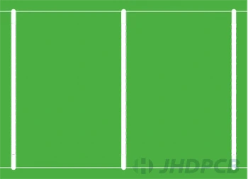
Rule 4: Milled panels with positive bridges
For milled panels with positive bridges there will be small overhangs left on the edge of the board after separation. This variant is more advantageous in the process of producing printed circuit boards. But compared to milled panels with negative bridges, it is not suitable for precise fitting in enclosures.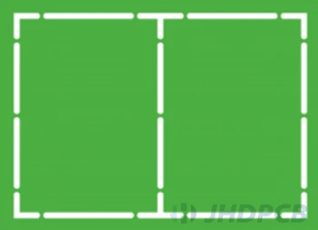
Rule 5: Milling panels for perforation drilling in residual bridges
If overhang on the board is not allowed due to the application, then the board is connected through a negative predetermined breakpoint. All conductor and copper areas shall have a minimum distance (blocking area) of ≥ 0.5mm from the outer contour.
The veneer should always be placed in the panel in one direction and should not be rotated 90°, otherwise it will cause a series of problems in the subsequent production process. For example, SMT wave soldering can create solder bridges if the preferred component alignment is not maintained. All boards should (if possible) have at least four bridges.
Rule 6: Mix Multiplier Panel
Hybrid multiplier boards are combinations of different board layouts on one panel. Printed circuit boards need to be scored or milled.
Please note that for panels to be milled, there must be a distance of ≥ 2.00 mm between the circuit boards. Yet, we recommend keeping a distance of 10 mm as a best practice.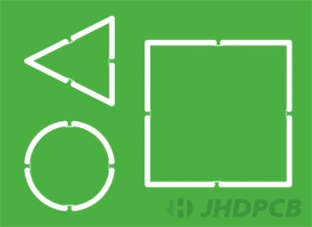
Rule 7: It is common to make a pair of boards (different designs) as a single set (customer panel PCB). Therefore, it makes sense to combine them. There may be some limitations to this:
- Boards should be similar in size to a valid panel.
- Most of the board parameters must be identical.
The distribution of copper needs to be similar, otherwise failures in the etch process may occur and the panel will warp in the reflow oven.
Rule 8: There must be a 0.05″ clearance between the component and any V-groove, in order to keep the component unaffected during the cutting process.
To make sure the knives don’t interfere with them, taller components need to be placed farther apart. For instance, there must be kept at least 1/8 inches between the score line and surface mount multilayer ceramic chip capacitors. If a component with a larger connection area is placed too close to the V-groove, then the split-board stress can break the solder joint. So they must be placed away from the grooves.
Rule 9: Knock-outs. If there are holes greater than 0.6 inches in your PCB design, in order to prevent issues in the process of wave-solder, may require a place holder, or knockout. Owing to PCB arrays are easier to sag in middle of an array, knockouts are very important in it. Larger, more irregularly shaped knockout holes require multiple three-hole piercing tabs. Smaller, regular-shaped rectangular knockouts may only require a wide five-hole piercing tab on one side.
Rule 10: Tab Placement. It is very important for tab placement to matain the integrity of PCB array design. Five-hole pierced joints must be placed every 2 to 3 inches along the edge of the board. Whereas, three-hole pierced fittings must place fittings every 1.5 inches. To avoid board edge bending, labels should be placed as close to the edge as possible, but not under overhanging components. To support the board, the designer must ensure that the lugs are large enough, but not so large that they interfere with the breakout process.
Rule 11: Perforation Placement. Remember not to place the label perforation below the very center of the label if you want to avoid protruding from the sides of the board. Instead, place them close to the edge of the PCB. On each side of the label if it is going to be placed between two PCBs.
Rule 12: Array Arrangement. In order to keep the break line consistent across the array, when the designer lays out the PCB, make sure that all the tabs that break off at one time are on the same line. If the fault lines are inconsistent, some tabs will simply be pulled perpendicular to the board surface while others will break, potentially causing the laminate to tear.
Rule 13: Detailed description the largest size panel that the machine can process.
Rule 14: In order to prevent the panel corner from breaking the seal when vacuum packaging the PCB panel, a radius needs to be placed on the panel corner.
Rule 15: Add tooling holes to the edges according to the needs of the machine. Four benchmark holes are opened at the corners of the outer frame. The strength of the holes must be appropriate to ensure that they will not break during the manufacturing process. The diameter and position of the hole should be accurate, and the hole wall should be smooth and free of burrs.
Rule 16: To be able to perform this process with high precision, fiducial markers need to be added so that vision within the various machines can give the system an accurate idea of where the PCB is. In order for the machine to determine if the PCB is loaded incorrectly, it is standard practice to add three reference points in the three corners on either side of the PCB when the PCB is aligned with the machine.
Rule 17: The shape and size of the board will dictate how many breakout tabs to use.Too much will complicate the panel removal process. Too little and the PCB may not be mechanically stable enough for assembly.
Rule 18: Exposing metal during routing or V-scoring may cause jagged edges and shorts after assembly.
Rule 19: To make it easier to remove the PCB circuit from the panel after assembly, it is necessary to chain drill in the panel scrap area.
Rule 20: When setting the reference point, usually leave a solder-free area larger than 1.5mm around the reference mark.
Rule 21:The shape of the panel should be as close as possible to a square or rectangle.
Rule 22:The outer frame of the panel should be a closed-loop type to ensure that the PCB panel will not be deformed after being fixed on the fixture.
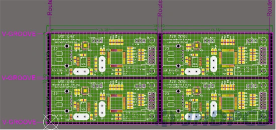
Step 1:
First, determine the dimensions of the circuit board. It can be viewed in Report > Board information. As shown below, this board is used as an example PCB board and measures 75 x 30mm. We will spell out a 2×2 PCB array in the new PCB.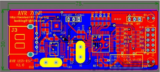
Step 2:
Using File > New > PCB to establish a rectangular PCB with measurements 160 x 65mm, with 2 signal layers, no power planes and vias.
Step 3:
On the newly created PCB model, click Place > Embedded Board Array/Panelize. As shown in the figure below.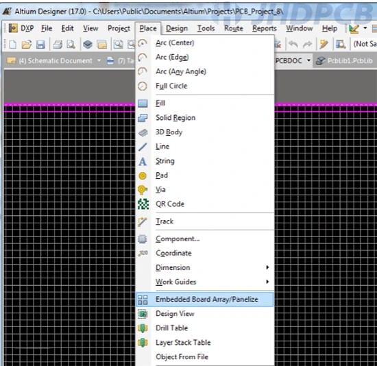
This is panel function. After clicking in, refer to the figure below, you need to enter the length and width in the Embedded Board Array window (this parameter is always slightly larger than the original board, it depends on your needs). In the PCB Document column, select the PCB file of the board to be assembled. Then you need to enter the number of horizontal and vertical rows to be spliced in the rows and columns of Column Count and Row Count respectively. Pick 2 of each here.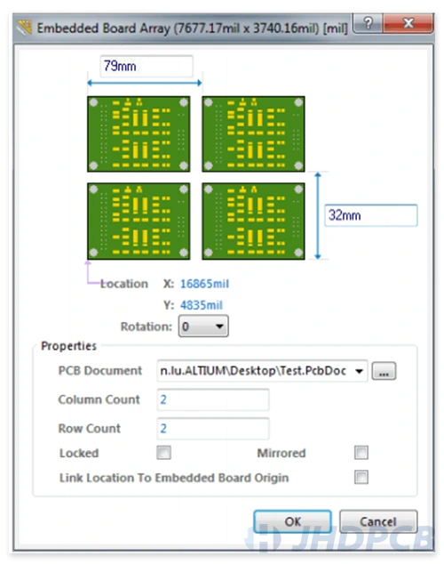
Step 4:
After the above parameters are set, click OK button to place the array board on the PCB. Then adjust the position to be just right. And reposition the origin of the PCB to the origin of the array board.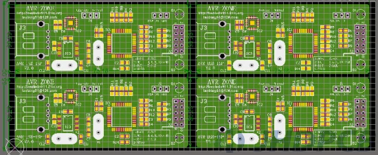
Step 5:
Enter the layer color manager below. After that, rename Mechanical2 to Route Cutter Tool Layer and define the line drawn on this layer as milling cutter milling PCB traces; rename mechanical 5 to FabNotes, and the line drawn on this layer is defined as Wash trace of the V -groove (V-GROOVE) on the PCB.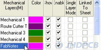
Please note that we need to draw Route Cutter Tool Layer traces and FabNotes traces on the PCB array board. We need to communicate our specific needs and intentions to the designers who process the PCB circuit board (CAM). But whether to use cut or V groove depends on the communication between us and the engineer of the board factory. The last step is to convert the PCB array board into a processing drawing file such as Gerber. Then submit the file to the JHDPCB, and communicate with the board factory about the specific process requirements and details.