wave soldering reflow soldering

Wave and Reflow Soldering in PCB Soldering: Process Guide

directory

As electronic products have become an indispensable part of our daily lives, the demand for printed circuit boards (PCBs) has increased dramatically. PCBs are essential components in electronic devices, and their quality directly affects the performance and reliability of the final product. Among the many manufacturing techniques, wave soldering and reflow soldering are two of the most commonly used methods in PCB production.
Wave soldering and reflow soldering are critical processes in the PCB assembly process. They play a crucial role in ensuring the reliability and stability of electronic products. As a professional PCB manufacturer, JHDPCB has been dedicated to providing high-quality PCBs for various industries, including automotive, industrial control, and consumer electronics. With advanced technology and equipment, we have the expertise to handle various PCB assembly processes, including wave soldering and reflow soldering.
In this blog post, we will explore the differences between wave soldering and reflow soldering, their advantages and disadvantages, and how to choose the best method for your specific PCB assembly needs. We will also discuss the importance of quality assurance in PCB production, including the relevant certifications and standards that JHDPCB has obtained. With our professional services and commitment to quality, we are confident that we can provide our customers with the best PCB solutions for their diverse needs.

What is wave soldering?

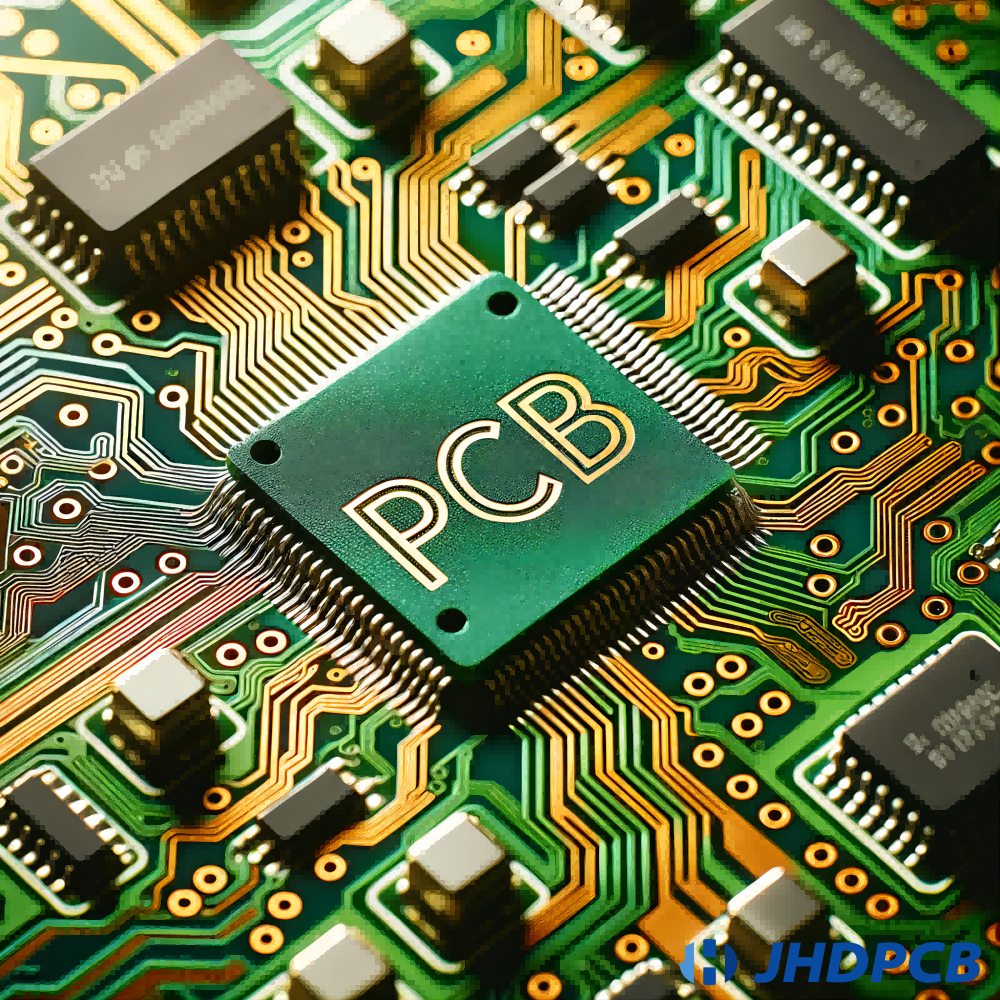
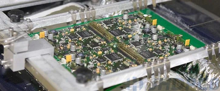
Wave solder is a batch soldering process used in printed circuit board manufacturing.The circuit board goes through a plate of melted solder, in which the solder produced by the pump surges upwards and looks like standing waves.The circuit board is in contact with this wave to solder the components to the circuit board.Through-hole printed circuit assemblies and surface mounting can both be soldered using the wave soldering technique.For the latter, the placement device glues the component to the surface of the printed circuit board (PCB) and then begins to melt the solder wave.This is called smt wave soldering.Miniature wave soldering is aimed at locally selective welding with high welding accuracy, while the primary purpose of wave soldering is to solder through-hole components, although surface-mounted components can also be soldered using this method.
Since through-hole components are almost superseded by surface-mount components, wave soldering is also give away to reflow soldering in many large electronic applications.Nevertheless, wave soldering still plays an important role in situations where surface-mount technology (SMT) is not viable or sufficient, such as with large power devices and connectors with high pin counts, or in cases where simple through-hole technology is predominant, such as with some major household appliances.

wave soldering

Application Field of wave slodering.

Wave soldering is a specialized soldering technique involved in the manufacture of printed circuit boards (PCBs).The process involves connecting the board to the PCB through a wave of melted solder. Areas of application for wave soldering include:

  1. Electronics Manufacturing:Wave soldering technology is a commonly employed method in the electronics sector for producing PCBs utilized in various industries such as consumer electronics, automotive electronics, telecommunications, aerospace, and defense.
  2. Industrial automation:The wave soldering machine plays a crucial role in the process of industrial automation as it is essential for achieving high-quality mass production.
  3. Medical devices:Wave soldering finds extensive application in the production of medical devices, including imaging systems, life support equipment, implantable devices, and more, which demand superior reliability and quality standards.
  4. Lighting industry:The manufacture of LED panels in the lighting industry involves utilizing wave soldering, which demands accurate soldering techniques to1. make certain superior durability and reliability.
  5. Automotive industry:The automotive sector employs wave soldering during the production of electronic components, including printed circuit boards for controlling systems, managing engines, and entertainment systems in cars.

In conclusion, wave soldering is a significant technology that plays a key role in the manufacture of electronic devices and components used in the modern world. Commonly used in THT (through-hole technology), DIP (dual in-line package) assembly. Of course, surface mount technology also uses wave soldering processes.

How to do wave soldering?

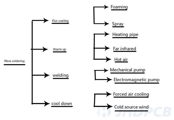
The steps of diy wave soldering include the following aspects:

Wave Soldering Process

To ensure that the soldering area is free from oxidation and other contaminants, flux is necessary. There are two types of flux: Flux can be categorized into two types: corrosive and non-corrosive. Non-corrosive fluxes require the surface to be pre-cleaned and are used when low acid levels are needed.Corrosive fluxes work quickly, demand minimal pre-cleaning, but are highly acidic.
The flux is applied to the bottom side of the board that requires soldering. Precise control of the amount of flux applied is crucial – insufficient flux can lead to suboptimal joints, while an excess may leave unwanted residues on the board.
There exist two primary approaches for applying flux:

  1. Spraying flux involves coating the underside of the board to be soldered with a fine mist of flux. In certain setups, an air jet may be used to eliminate any surplus flux.
  2. Foam flux is applied by passing the electronic printed circuit board through a flux foam cascading head. The foam is generated using a tank of flux and a plastic cylinder with small perforations that are submerged in the solution. The metal chimney covers the plastic cylinder, and air is pushed through it, which causes the flux foam to ascend inside the chimney.

Click to view more detailed flux knowledge.

During the wave soldering process, the printed circuit boards and devices are subjected to significantly greater heat levels than those encountered in manual soldering. This thermal shock may lead to a notable rise in failure rates. The most effective solution is to preheat the boards to stabilize them at the desired temperature, thereby reducing the negative impact of the sudden temperature change.
During the preheating stage, hot air heaters are typically employed to blow hot air onto the circuit boards as they pass through the wave soldering machine. For boards with high component density, an infrared heater may be employed in addition. This approach ensures uniform heating across all boards and eliminates any areas that might be shaded from the heat.
The preheating temperature is typically established between 90-110 degrees, following these guidelines:

  • For single-sided wave soldering/mixed assemblies, the temperature should range from 90 to 100 degrees.
  • For double-sided wave soldering/mixed assemblies, the wave soldering temperature should be between 100 and 110 degrees.
  • Double-sided reflow soldering requires that the temperature be set in the 100-110 degree range.
  • Multilayered PCB wave soldering/mixed assemblies require a higher temperature range of 115-125 degrees.
  • Similarly, multilayered PCB reflow soldering will necessitate temperatures between 115 and 125 degrees.

When establishing the wave soldering process, it’s essential to evaluate the solder wave’s height, as it is a vital parameter. The contact time between the components being soldered and the wave of solder is generally set to last between 2 to 4 seconds. Two parameters on the machine control the contact time: the conveyor speed and the wave height. Adjusting either parameter will result in a modification of the contact time.

Normally, the height of the wave in a wave soldering machine can be adjusted by changing the speed of the pump on the equipment.To obtain a more detailed record, a tempered glass plate can be employed to assess and detect any changes. Additionally, if there is a fixture, the contact time, height, and speed can be digitally documented.
The role that wave soldering plays after the formation process is significant. As the temperature continues to rise, the solidified solder paste liquifies, creating waves that result in the molten metal alloy adhering to the pins and pads, forming an electrical connection. This process ensures that the components are firmly bonded to the board.

Controlling the cooling rate of the PCB is crucial after the soldering process. Swift cooling can cause the PCB to distort and harm the integrity of the solder joints. Conversely, slow cooling can lead to the PCB becoming fragile and certain components getting damaged by excessive heat. To minimize the risks of PCB damage, it is recommended to use either air or water cooling to achieve an optimal cooling rate.

To mitigate any potential issues that could affect customers, it is crucial to conduct visual inspections and AOI machine tests on the assembled boards following the soldering process. Although reflow soldering has largely replaced wave soldering, having a wave soldering machine remains an essential component for each PCB assembly plant, as this assembly technology cannot be entirely substituted.

What is reflow soldering?

Reflow soldering is a process that utilizes a combination of flux and powdered solder, which is referred to as solder paste. This method temporarily attaches small electrical components to their corresponding contact pads. The entire assembly is then exposed to controlled heat, causing the solder paste to reflow and create long-lasting solder joints. This heating process can be achieved by passing the assembly through an infrared lamp or reflow oven, or by individually soldering each joint with a desoldering hot air pencil. Hot bar reflow soldering is a method that utilizes a hot head to apply heat and force in order to achieve the simultaneous heating and soldering of multiple connections.

Reflow ovens are the preferred method for soldering surface mount technology components (SMT) onto a printed circuit board (PCB). Benchtop reflow soldering is the process of conducting small-scale surface mount technology (SMT) reflow soldering within a space that is the size of a tabletop. In these ovens, each segment has a temperature that is regulated according to the specific thermal requirements of the assembly being soldered. Reflow ovens designed for soldering surface mount components are also capable of soldering through-hole components by filling the holes with solder paste and inserting the component leads through them.In contrast, wave soldering has traditionally been used to solder multileaded through-hole components onto a PCB primarily designed for surface-mount components.

How to do reflow soldering?

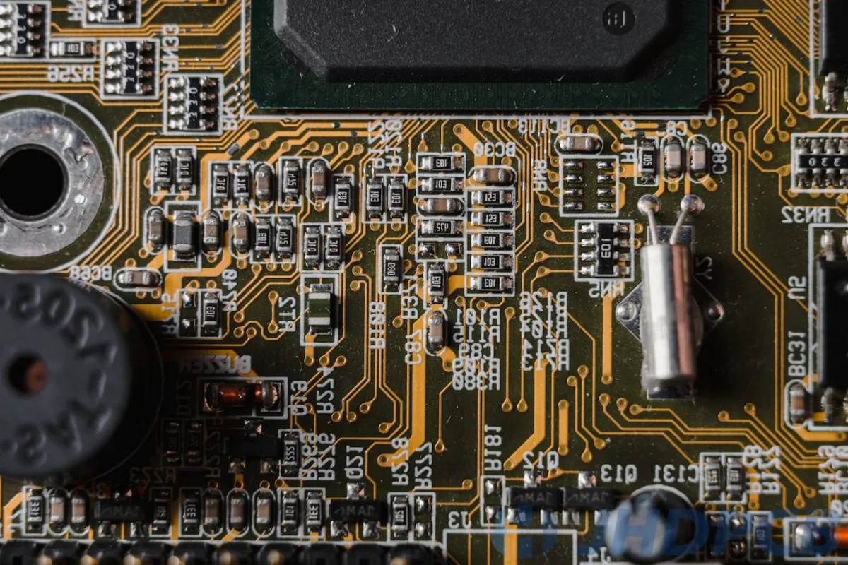
During the reflow soldering process, a mixture of solder and flux known as solder paste is applied to the pads. Components are then placed onto the solder paste, creating a temporary connection. The PCB is subsequently heated in an oven using hot air, infrared radiation, or other forms of heat radiation. The oven temperature is carefully monitored and controlled to ensure that the solder paste melts and solidifies, forming stable solder joints. 

  • The typical flow for single-sided mounting involves the following steps:
    solder paste printing > pick-and-place >reflow soldering > inspection.
  • For double-sided mounting, the process includes the following steps:
    solder paste printing on the A-side > pick-and-place > reflow soldering > solder paste printing on the B-side > another pick-and-place > another round of reflow soldering > finally inspection.

    Reflow Soldering Process

The reflow soldering process consists of several crucial steps, each of which is necessary to ensure that the board is heated to the correct temperature without requiring any adjustments or thermal shocks. Maintaining the proper temperature in the reflow chamber or tunnel is critical for producing high-quality solder joints. The steps of diy reflow soldering include the following aspects:

  • Preheat
    It is crucial to ensure that the board is exposed to the appropriate temperature during reflow soldering. If the temperature is too high, there is a risk that the board’s components or the board itself may be damaged due to thermal stress. Similarly, introducing the board to the temperature too rapidly can result in certain areas not receiving the required amount of heat due to thermal mass. Conversely, if the board is introduced too slowly, it may be difficult to achieve the desired temperature. Generally, the recommended temperature increase rate for infrared reflow soldering is between 2-3 degrees/sec, although this rate can occasionally be adjusted to 1 degree/sec.
  • Thermal soak
    Following the board’s exposure to the right temperature, the subsequent step is commonly referred to as thermal soaking. This process involves maintaining the board at the optimal temperature for a set period. There are several reasons for thermal soaking. Firstly, it ensures that any sections of the board that were not adequately heated due to shadowing are brought up to the correct temperature. Secondly, it eliminates any solvents or volatile content from the solder paste and activates the flux. The soak phase typically lasts anywhere from 60 to 120 seconds, depending on the mass differential of the assembly and the types of components present. The duration of the soak can be shortened if heat transfer during this phase is more efficient.
  • Reflow
    The reflow stage is the crucial part of the soldering process where the desired temperature is attained, and the solder melts to form the required joints. During this stage, the flux works to reduce surface tension, particularly at the metal junctions, to facilitate a metallurgical bond.
  • Cooling
    The final step of the soldering process is to cool the board down, and it must be done carefully to prevent stress on the components. Effective cooling is essential to avoid the formation of thermal shock and excessive intermetallic compounds. Typically, cooling takes place in an area with a temperature range of 86-212 degrees Fahrenheit. This temperature range allows for rapid cooling while ensuring that strong joints are formed.

What's the difference between reflow and wave soldering?

The dissimilarities between wave soldering and reflow soldering are significant, and it is crucial to understand the distinctions before choosing which method to use in PCB assembly services. Any alterations made to the soldering process can result in changes to the entire manufacturing process, including production efficiency, costs, time-to-market, profits, among others.
Wave soldering and reflow soldering have notable distinctions in their core soldering process.

  • Complexity:
    In terms of complexity, wave soldering is considerably more intricate. The process involves placing the board on a conveyor belt to pass over the solder wave, which requires careful handling and adjustments to achieve optimal results. The worker or handler must have expertise in the process. In contrast, reflow soldering is a much simpler process.
  • Environmental conditions:
    Environmental conditions are vital in both wave and reflow soldering processes as any fluctuations can affect the quality of solder joints. However, in reflow soldering, maintaining all the conditions can be challenging. The wave of solder must be in optimal environmental conditions to function correctly. Reflow soldering involves careful preheating of the board under controlled conditions before applying the molten solder at the required temperature to ensure optimal fluidity. Temperature shifts during this process can result in defects and imperfections in the soldering, highlighting the importance of stable environmental conditions.
    Compared to wave soldering, it is simpler to maintain the necessary conditions for reflow soldering as the reflow oven only needs to melt the solder in the paste, making controlling the environmental factors easier.
  • Constraints:
    In both wave and reflow soldering, there are constraints beyond just temperature that must be carefully controlled. The quality of the soldering in reflow soldering is influenced by the length of time that the board is subjected to heat. The timing must be precise, as exceeding the limits can result in excess solder or insufficient solder for some components. Maintaining the correct pad shape, size, and orientation is also crucial in wave soldering. Controlling the exposure time in reflow soldering is also necessary, but it is comparatively easier than wave soldering.
  • Speed:
    Wave soldering is a faster process than reflow soldering, making it the preferred choice for high-volume PCB production. This is because in wave soldering, the flux is sprayed, and the PCBs pass over the solder wave quickly. Nonetheless, the use of a stencil to apply solder paste and the requisite extended exposure of the PCB inside the reflow oven during reflow soldering can lead to time-consuming processing.
  • Cost:
    When it comes to cost, wave soldering is a more economical choice than reflow soldering, particularly for large volume orders. Reflow soldering is a more expensive option due to the need for special stencil production and the higher cost of the reflow oven compared to a wave soldering machine.
  • Usage:
    Through-hole components are ideally suited for wave soldering, while SMDs are better suited for reflow soldering.
Reflow Soldering vs Wave Soldering
Reflow SolderingWave Soldering
Reflow soldering is a less complex technique.As compared to the reflow soldering, the wave soldering technique is more complex.
Reflow soldering is soldering the components, with the help of reflow, which is formed by hot air.In wave soldering, the components are soldered, with the help of wave crest, which is formed by a melted solder.
As compared to wave soldering, this soldering technique is slower, and also more expensive.Wave soldering method takes lesser time for soldering PCBs, and is cheaper compared to other techniques, too.
It requires no specific controlled environment, thus offers lots of flexibility, while designing or manufacturing printed circuit boards.Careful monitoring of issues, such as the temperature of the board, and time that it spends in the solder is necessary. If the wave soldering environment is not maintained properly, then it can lead to defects in the board design.
Unlike wave soldering, this soldering method is implemented, when less number of circuit boards are required to be manufactured.This method is mainly used if bulk soldering is required. It helps manufacture a number of printed circuit boards in a less amount of time.
It is not mandatory to consider factors, such as board orientation, pad shape, and sizes, and shadowing, as that in wave soldering.You are required to take into account different factors, including pad shapes, and sizes, layout, heat sinking, and placement for effective soldering and better results.
Reflow soldering is ideal for soldering surface mount devices on the printed circuit board.If through-hole components are to be soldered, then wave soldering is the best suited technique to opt for.

What factors control the quality of wave/reflow soldering?

Reflow and wave soldering have different process conditions, but both are critical to achieve good solder joints.The following are essential process conditions to consider:

  • Temperature:
    The temperature must be high enough to melt the solder and form a reliable solder joint. For wave soldering, the typical temperature range is between 240°C and 260°C, while for reflow soldering, it ranges from 220°C to 240°C.
  • Atmosphere:
    The atmosphere inside the soldering oven must be inert and free from oxygen and moisture, typically achieved by using nitrogen gas. Nitrogen reflow soldering is a method of soldering that utilizes pure nitrogen in a reflow oven.
  • Time:
    Wave soldering has a relatively constant time interval, while reflow soldering depends on the size of the component being soldered and is calculated based on ramp rate and hold time.
  • Flux:
    Flux is required to remove oxides from the surface of the component or PCB, enabling better wetting of the solder and improved solder joints.
  • Solder paste:
    Solder paste is a mixture of solder and flux applied to PCB surface-mount pads, melted during reflow soldering to form a solder joint. Proper use of solder paste enhances process consistency and simplifies solder joint quality.
  • Conveyor speed:
    Conveyor speed is crucial in maintaining the appropriate dwell time of components and achieving good solder joints.
  • Component placement:
    Components must be correctly placed on the PCB, with sufficient spacing to avoid shorts and attain adequate solder joint formation. If you want to know more about PCB components, you can check our related articles.
  • Cleaning:
    Thorough cleaning of PCB and components is necessary to prevent contaminants that hinder good solder joint formation.
  • High-quality PCB stencil:
    A PCB stencil made of stainless steel with laser-cut openings accurately deposits the right amount of solder on the technology pads, resulting in perfect alignment and excellent mechanical strength and electrical connections for users.

What precautions should be taken when doing manual wave/reflow soldering?

To ensure your safety when performing wave/reflow soldering, it is crucial to follow the guidelines provided by your employer, local and state laws, and equipment manufacturers regarding proper safety protocols and precautions. However, you can take general precautions to enhance your safety, including:

Soldering Iron:

  • Avoid touching the element of the soldering iron, which can reach temperatures of up to 400°C.
  • Instead of using your bare hands, employ tweezers or clamps to hold the wires that need to be heated.
  • Keep the cleaning sponge moist during usage.
  • When not in use, store the soldering iron in its stand and avoid placing it on the workbench.
  • Turn off and disconnect the device when not in use.

Solder, flux, and cleaners: 

  • Wear eye protection to prevent injuries from solder “spitting”.
  • Whenever possible, use rosin-free and lead-free solders.
  • Dispense cleaning solvents from bottles.
  • After soldering, wash your hands with soap and water.

Lead exposure:

  • Lead can cause severe health effects if ingested accidentally. Wear gloves when in direct contact with solder.
  • Soldering may generate limited fumes that contain lead.

Rosin exposure: 

  • Rosin is a resin in solder flux that produces visible fumes during soldering, leading to eye, throat, and lung irritation, nose bleeds, and headaches.
  • Repeated exposure to rosin can cause respiratory and skin sensitization, exacerbating asthma.
  • Rosin is a significant occupational health hazard.

Ensure personal protection: It is crucial to wear appropriate protective gear such as goggles, gloves, and clothing to prevent injuries during wave/reflow soldering.
Maintain a clean, obstruction-free work area: Keep your work area clean and unobstructed to prevent accidents.
Use correct equipment: Always use proper equipment that meets safety standards, and conduct regular maintenance checks.
Follow manufacturer’s instructions: Adhere to the manufacturer’s instructions when operating soldering equipment to minimize accidents.
Keep a first aid kit nearby: In case of an injury, keep a readily available first aid kit and ensure someone trained in administering first aid is present.
Proper ventilation: Ensure proper ventilation at your workplace as wave and reflow soldering produce harmful fumes.
Prevent fire hazards: Avoid placing flammable objects such as paper, plastics, and liquids near the soldering equipment to prevent fire.
Provide training and supervision: The supervisor/line manager should educate the user regarding the dangers of welding, implement effective controls, and enforce their proper use. All welds should receive proper training and supervision.
Ensure electrical safety:To guarantee electrical safety, make sure to utilize soldering irons that have no apparent damage to the body, cable, or plug. Furthermore, all soldering irons must have undergone electrical safety (PAT) testing within the past twelve months. Also, keep the soldering station free of cables to prevent damage to the heating tip. If a short circuit is possible, use a grounding socket and grounding pin.
Dispose of waste properly: Collect waste solder in containers with lids and label them hazardous waste.Dispose of used solder sponges and contaminated rags by placing them in sealable bags and appropriately discarding them.
Remember safety at all times: Always prioritize safety, follow safety procedures, and ensure you are working under safe conditions.

Frequently Asked Questions.

  1. Mass Production – With the exception of the smallest production batches, reflow soldering cannot match the speed of wave soldering.
  2. Cost Extension – Due to its comparative speed advantage, the cost of wave soldering per circuit board is lower than that of reflow soldering.
  3. Through Hole Components – Wave soldering remains the sole method for soldering through-hole components, despite the fact that many can now be replaced with SMD packages. As a result, there are still numerous power components in through-hole configurations, representing a significant market for circuit boards that require wave soldering.
  1. Limited component compatibility: The compatibility of components is restricted when it comes to wave soldering since the high temperature of the solder peak can potentially harm sensitive elements like connectors, diodes, and electromechanical switches.
  2. Time-consuming setup: There are many steps to prepare wave soldering PCB, which requires board cleaning, welding hood, and fixture preparation. Using this process not only requires a substantial amount of time but also results in an augmented production expenditure.
  3. Lack of precision: In contrast to selective soldering, wave soldering lacks the ability to perform precise soldering, resulting in potential reliability problems and product defects due to some components being inadequately or excessively soldered.
  4. Solder bridges and shorts: If the solder wave does not flow correctly between the pads of the PCB during the wave soldering process, it may cause solder bridges and shorts, resulting in short circuits and functional problems in the final product.
  5. Environmental concerns: Environmental issues arise from the materials used in wave soldering, such as cleaning chemicals and flux, which could potentially harm the environment and therefore require appropriate disposal measures.
  1. High-quality solder joints: Reflow soldering produces uniform, reliable and precise solder joints that are of high quality. Proper pin to hole ratio is crucial to ensure the quality and reliability of through-hole joints during wave soldering.
  2. Increased efficiency: Reflow soldering is a more efficient and faster process compared to manual soldering, as it can be automated and handle higher volumes of production in less time.
  3. Cost-effectiveness: Integration of reflow soldering with other processes, such as surface mount technology (SMT), reduces assembly costs and minimizes inventory costs.
  4. Reduced environmental impact: Lead-free reflow soldering reduces the environmental impact of manufacturing by eliminating lead contamination.
  5. Improved precision: Heat is used to melt the solder paste during reflow soldering, making it possible to precisely control the temperature for each component.
  6. Compatibility with a range of components: Reflow soldering is compatible with a wide range of components, including small components such as surface mount devices (SMD), ball grid arrays (BGA) and quad flat packages (QFP). SMD reflow soldering is a soldering process used for attaching surface mount components to printed circuit boards (PCB).
  7. Reduced rework: Consistent, high-quality solder joints produced by reflow soldering can reduce the need for rework and remanufacturing.
  • Cold Solder Joint (dull joint): A poorly wetted solder connection after soldering results in a dull, grayish appearance, which is a common reflow soldering defect. It is caused by insufficient heat to reflow the solder adequately. Possible solutions include setting a maximum reflow temperature high enough for the material, accelerating the cooling rate after reflow, and minimizing vibrations during and after reflow.
  • Non-wetting: This occurs when molten solder fails to adhere to the surface it contacts, leaving none or only parts of the solder adhered. Long soak times during reflow may be contributing to this problem, as well as insufficient heat during the process, preventing the flux from reaching its activation temperature.
  • Solder Balling: Solder balling refers to tiny spheres of solder that form separately from the main body of solder in the joint. Moisture-contaminated solder paste during reflow can cause solder balls, which are left behind when moisture splatters.
  • Tombstoning: This soldering defect occurs when force imbalances during reflow cause a chip component to pull into a vertical position with only one terminal connected to the PCB. Tombstoning can result from an uneven heating process, causing a temperature difference at the component terminals where one side reflows before the other, leading to the remaining lead standing upright.

Wave soldering is not suitable for surface-mounted components, and other techniques like infra-red reflow soldering are preferred. Due to advancements in soldering technology and the availability of alternative methods, wave soldering has lost its popularity and is being used less frequently nowadays.

A sudden increase in board temperature can cause thermal shock and lead to board failure. To prevent this, the board undergoes preheating to increase its temperature gradually.

The reflow temperature of the solder varies depending on the mixture. In the case of lead-free solder, it is standard to have a reflow temperature ranging from 240 to 250°C, with a duration of 40 to 80 seconds at temperatures above 220°C. Minor temperature changes do not affect soldering with lead-free solders.

Although it is feasible to perform reflow soldering with a heat gun, the method is somewhat slow and not suitable for assembling a large number of electrical components on a board.

After soldering a joint, wait for it to cool down. Avoid touching the joint using your hand. Instead, use a magnifying glass to inspect the joint.The solder connection should appear lustrous and fit snugly into the copper pad.

Now that you understand the differences between wave soldering and reflow soldering, you can decide which is better for your project. If you wish to stay abreast of the latest technological advancements, using wave soldering could be a suitable option.However, if you prefer traditional methods and don’t mind extra steps, reflow soldering might suit you better. The choice is yours.
JHDPCB is a top enterprise in PCB board design and manufacturing. We offer four main advantages: reliable quality, lower cost, quick delivery, and a professional team. Our experience in optimizing wave and reflow profiles allows us to minimize rework and improve board quality. If you’d like to learn more or work with us on your next project, please contact us!

Get a PCB Quote Now

Open high-quality PCB manufacturing services in JHDPCB

Leave a Comment