Single & Double Layer PCB

Single & Double-Layer PCB

Single & Double Layer PCB is the most used in the market,the market demand is huge. So it is important to find a supplier with a large production scale. JHDPCB  is China’s top 5 single-sided and double-sided  PCB manufacturers, and is equipped with 4 fully automated single layer PCB production lines and 4 fully automated double-layer production lines. Monthly capacity up to 500,000 m². We can reduce costs and provide customers with the most cost-effective PCB by large-scale production.Next, JHDPCB will take you to learn more about Single & Double Layer PCB.

Single-&-Double-Layer-PCB2

What are Single & Double-layer PCBs?

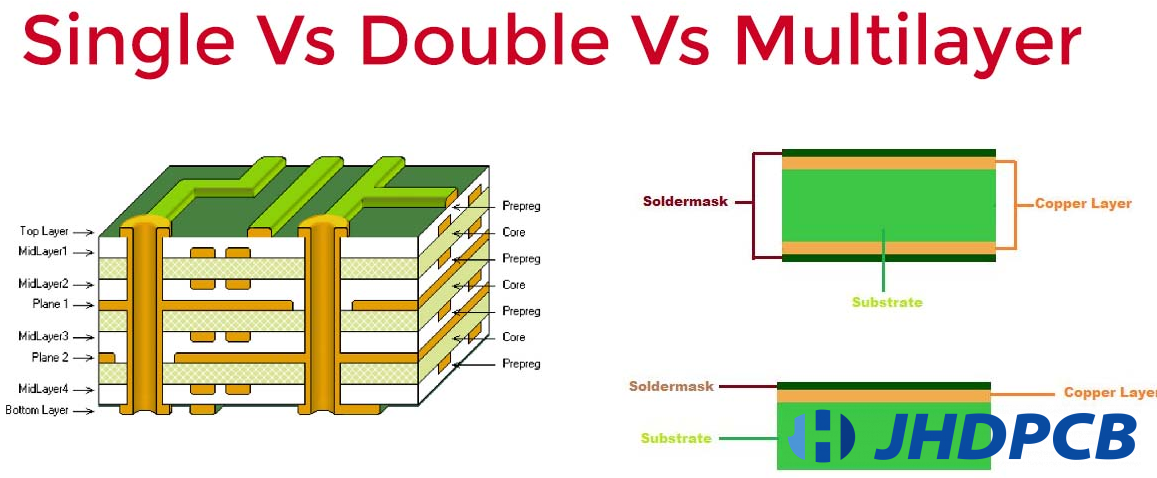
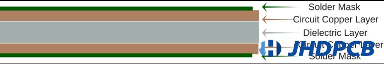
The strength or rigidity of the printed circuit board comes from the core and the substrate. The materials of substrate are usually aluminum or glass fiber and the core is basically epoxy-reinforced fiberglass cloth. The manufacturer glues thin copper foil on the top or both sides of the core to form a copper cladding. The single layer PCB has only one layer of copper, while the double-sided layer PCB is covered with copper on both sides. The copper layer will be covered with a layer of solder mask to prevent oxidation of the copper. Different substrates constitute different PCB types, such as aluminum PCB or LED PCB,  MCPCB, high TG PCB, FR-4 PCB, Heavy Copper pcb, CEM-3 PCB, etc. JHDPCB has established long-term cooperative relations with many well-known CCL factories, can produce various types of PCBs. For specific CCL types available, please refer to “CCL that JHDPCB can provide

What are the advantages of Single & Double-layer PCBs?

Easily Design and Production:Single layer PCB & Double-layer PCB are relatively simple and are also very common, which means most designers can easily design them, and most manufacturers can produce them without problem. The design and production processes will be easy compared to advanced printed circuit boards(means Multilayer PCB,HDI PCB and etc.)

Lower cost: Because single & double-layer PCBs are simple. They require fewer resources, less time and less expertise to design and produce. This makes them less expensive. Therefore, lower cost is one of Single & Double-layer PCBs significant benefits, especially for high volume orders. JHDPCB can provide our customers with competitive prices through large-scale mass production.

Faster Lead Times: With their simple and uncomplicated construction, single & double-layer PCBs are easy to fabricate.We can deliver within a week even for very large orders. For some very urgent small batch orders, we can deliver in one day.You can visit our Our Standard Build Time for reference.

More alternative PCB Materials: There are more alternative PCB materials for single & double-layer PCBs. Such as FR1,FR-4, Aluminium,CEM1,CEM3. The customers can choose the material according to their needs and budget.

JHD advantages in Single & Double-layer PCBs

Large-scale production:Equipped with 4 fully automated single layer PCB production lines and 4 fully automated double-layer production lines. We can reduce costs and provide customers with the most cost-effective PCB by large-scale production.

 Excellent procurement supply chain management: We reduce our material costs through centralized procurement and large-scale procurement.

 Experienced team of experts: We have been deeply engaged in Single & Double-layer PCBs production for more than 12 years, supported by an experienced team of experts that can provide our customers with reliable quality PCB.

 Quick delivery: In order to shorten the delivery time, We have many brand laminates in stock, such as aluminum, cem1/cem3,FR4, and copper clad laminates. At the same time, we have a perfect logistics system, which can quickly connect express delivery, air shipping, train shipping, sea shipping and other logistics. For more information please refer to TRANSPORT DELIVERY .

 Learn more about  JHDPCB’ Advantages

The well-known and reliable CCL(Copper Clad Laminate)manufacturer we are cooperating
Company Laminate Datasheet
KINGBOARD(KB)

FR1

FR4

CEM1

KB-3151C

KB-6150/KB-6150C

KB-5150/KB-5150A/5150

SYTECH

FR4

CEM1

S1130

S3110

GOLDENMAX(GDM)

ALU.

CEM3

FR4

GF111&GF112

GC111&GC112

GL12&GL22

JINBAO ALU. HRA510
NANYA FR4 NP-150R

Some single side PCB and double sides PCB produced by JHD

JHD's single & double-sided PCB manufacturing capabilities.

Item Content Description
Material type: FR-1, FR-4,CEM-1,CEM-3,Copper base, Aluminum,Polyimide(PI)
Surface finish: ENIG gold, HASL(LF),OSP, Immersion Silver,Immersion Tin, Electroplated nickel gold,,ENEPIG
Layer No : Single side / Double side
Max PCB size: 1500mm*600mm
Min PCB size: 5mm*5mm
Min space/width: 0.1mm
Warp and Twist: ≤0.5%(board thickness:1.6mm,PCB size : 300mm*300mm)
Board thickness: 0.3-5.0mm
Copper thickness: 35um-240um
Outline Tolerance: ±0.15mm
V-CUT Precision: ±0.1mm
Capacity: 80000㎡/Month
PTH Dia tolerance: ±0.076mm
Outline tolerance: CNC :±0.1mm punch:±0.15mm
Min.Solder Mask Bridge: 4mil
Min.Line/Track Width: 3mil
MIN.Drilling Slot Size: 0.6mm
Solder Mask Color: Green, Black, Blue, White, Yellow, and Matt, etc.
Solder Mask Hardness: 6H
Flammability: 94v-0
Check out more detailed manufacturing capabilities.

What are the applications of Single & Double-layer PCBs?

Industrial machinery: Single & Double-layer PCBs are often used as part of powerful mechanical apparatus. Where the current 1 OZ copper PCB cannot meet the needs, heavy copper PCBs can be used. Cases where heavy copper PCBs have advantages include engine controllers, high-current battery chargers, and modern load analyzers.

Lighting: LED lighting has become popular due to its low power and high productivity, it replaces traditional energy-saving lamp lighting. So the aluminum PCBs used to make them also became popular and they got a dedicated name LED PCB. Aluminum PCBs are widely used in LED lamps because of their better heat dissipation performance and certain rigidity.

Power supplies: The power supply industry generally tends to use single or double layers PCB, because the circuit design of the power supply is relatively simple and can be realized with single or double layers PCB. For cost considerations, they have become the first choice. In addition, if FR4 PCB is used, it has better electrical insulation and is more suitable for power supply products.Please refer to Everything You Need to Know About PCB Power Supply Design for design suggestion.

Automotive industry: Automotive companies use adaptable PCBs designed to withstand the high vibration conditions common in this field, such as automotive dashboards. In addition, in order to obtain excellent heat dissipation performance, metal PCBs are more favored by automobile companies, such as circuit boards used in automobile headlights.

For details of single-sided PCB and double-sided PCB application fields, please understand below.

If you want to do 1 layer PCB prototype or 2 layer PCB prototype, please feel free to contact JHD Customer Service via email. We will provide you with high-quality PCB with rich experience and first-class precision equipment. Regardless of any type of PCB, PCB assembly, small or high volume needs, just send your Gerber file along with your material and quantity requirements and we’ll give you a price shortly. All PCB manufacturing processes comply with IPC Class 2 or Class 3 standards and ISO 9001:2015 certification, standardized production and sophisticated PCB testing processes will ensure that every product we deliver to our customers is of high quality.

content

What is a 1-layer PCB board?

Single-layer PCB, also known as single-sided PCB, refers to a printed circuit board with a single-layer conductive pattern. The circuit board is laminated with insulating material, and the electronic components on the other side are electrically connected and mechanically fixed.

Single layer PCB type.

1,Single-layer rigid PCB: It is a single-layer PCB made of rigid materials such as fiberglass. The circuit board prevents the circuit from breaking and bending which is not flexible. Now, they are used in various types of devices, such as driver and calculators.

2,Single-layer flexible PCB: A single-layer PCB is constructed of flexible material rather than rigid material. Single-layer flexible PCBs have many more advantages over one-layer rigid PCBs, but price are more expensive for manufacture. Click to view the detailed production knowledge of flexible PCB.

3,Single-layer high-frequency PCB: It’s the type of single layer PCBs which is used in high frequency PCB. The boards are made up of a Teflon or polyphenylene oxide (PPO) material. There are some tips you need to know when choosing high frequency one layer PCBs, such as thermal expansion, dielectric loss as well as water absorption and so on.

4,Single-layer rigid-flex PCB: It is a single-layer PCB composed of glass fiber and plastic. So single layer is related to plastic and fiberglass. Compared with single-layer rigid and flexible PCBs, they have many advantages, such as reducing the size and weight of the entire PCB. Click to view the detailed knowledge of rigid-flex PCB.

5, Single-layer aluminum PCB: It is a single-layer PCB type composed of aluminum material substrate. The design of the board is very similar to a copper backed PCB, with one difference, it uses an aluminum PCB substrate instead of copper. Because the aluminum back is used with the insulation material, the heat of the insulation material is transferred to the back. Years of production experience have made JHD a strong advantage in the production of aluminum-based PCBs. If you have aluminum PCB needs, you must not miss JHD.

CCL Single layer pcb Raw Material.

*Grade Fiberglass Laminates:FR1/Fr4;                *Metal:Aluminum/Copper base;                  *Polyimide / PI;
*CEM:Cem 1/Cem 3;                                                       *Ceramics
For detailed substrate information see “Introduction To The Material Properties Of PCB CCL

Single PCB structure.

A single PCB is primarily composed of pads, vias, mounting holes, circuits, components, connectors, filling, and electrical boundaries circuit board. 
The main functions of each part are as follows:

  • Pads: A metal hole for soldering component pins.
  • Via holes: A metal hole used to connect component pins between layers.
  • Mounting holes: used to fix the circuit board.
  • Circuits: Grid copper film used to connect component pins.
  • Connectors: Used to connect components between circuit boards.
  • Fillings: Copper plating for ground nets, which can effectively reduce impedance.
  • Electrical Boundaries: Used to determine the dimensions of the board; all components on the board must not exceed the boundaries.

1-Layer PCB Fabrication Process.

Cutting – Cleaning – Drilling – Cleaning – PTH – Panel – Plating – Cleaning – Photolithography – Image Transfer – Inspection – Copper/Tin – Plating – Coating – Removing/Etching/Tin – Removing – Inspection – Cleaning – Solder Mask – Exposure/Develop/Inspection – Prepreg – SilkScreen – HASL – Conformal – Coating – Post – Soldering – Cleaning – Test – Final Inspection – inner vacuum Packing – outer Packing

How to Make a Single Layer PCB? single layer pcb manufacturing.

Printed circuit boards (PCBs) provide hobbyists and electronics manufacturers a cost-effective method of laying out and connecting electronic components. Unlike ProtoBoard and PerfBoard, PCBs are custom made for each project, and if designed properly, there is no need to add any wires between copper wires to connect components. A single layer PCB is just with copper foil on top/bottom side and it’s made of fiberglass.

1. Lay out the electronic components on a breadboard or performance board. Double check the layout for errors against the schematic.
2. Adjust the components on the board until the layout size is correct or smaller than the PCB.
3. Start the graphic design or PCB layout software on the computer. start a document with the same length and width as the PCB.
4. Draw the circuit layout with software. Use 1/100″ to 5/100″ wide black wire for copper rails. For beginners, thicker circuits may be easier to work with. Use a circle to represent each drill hole on the board to accommodate a component. Each circle consists of a 3/100″ wide blank space in the middle and a 2/100″ thick stroke line around the circumference of the circle. The space in the circle indicates the size of the drilled hole. If using a drill bit wider or smaller than 3/100th of an inch, adjust the size of the circle to match the size of the drill bit.
5. Paste the name of the component to be soldered on each circle. Compare the circuit layout with the schematic to do correction.
JHD provides some suggestions on PCB design layout, hope it can help you.

6. Get a sheet of smooth tissue paper from a magazine or catalog – don’t use the cover. Choose a page with a white background such as a plain text page.
7. Use scissors to cut the magazine paper to size suitable for the printer.
8. Set the laser printer with best quality setting. Do not use Eco mode or any mode that reduces toner usage. When printing layouts, manually feed magazine paper through the printer to avoid paper jams. Alternatively, stick magazine paper onto regular printer paper and feed the paper into the printer.
9. Remove any excess paper around the corner of the printed layout.
10. Clean the copper side of the blank PCB with a kitchen scrubbing pad and water until shiny. Remove all dirt and oil from the circuit board, using soap if necessary. Avoid touching the copper with your fingers and wear clean gloves if necessary.
11. Empty the water from the iron and set the iron to the highest temperature. Close the steam and wait for it heating up.
12. Attach the PCB to a hard, flat surface with the copper side up. Do not put tape on the copper wire side.
13. Place the printing paper on top of the PCB with the print side down. Align the layout with the board so that it does not come off the edge of the board.
14. Press the iron firmly against the magazine paper and PCB for one minute. Use lots of pressure and don’t move the iron.
15. Iron the paper hard for four minutes. Move the iron slowly over the paper and PCB. Do not let the paper move. Wait for the board to cool down.
16. Fill a plastic container with cold water and also trim excess paper around the PCB and. Put the PCB in the water and wait for the paper to soften, this may take 5 minutes.
17. Peel or lightly wipe off the wet paper by hand. When done, you should be able to clearly see the layout on the copper side of the board.

18. Put on goggles, rubber gloves and a plastic apron.
19. Place hydrogen peroxide in a plastic container. Slowly pour in hydrochloric acid. Do not use metal containers as the mixture will corrode the metal. Use a well-ventilated space.
20. Carefully place the PCB into the mixture, copper side down, and using plastic pliers. Wait three to four minutes, then lift the board with pliers and check for dissolved copper around the track. If not, put the board back in the mixture and check every two to three minutes.
21. Use tweezers to remove the PCB from the mixture. Rinse with water.
22. Lightly soak a paper towel with paint thinner. Wipe the toner off the copper side of the board.
drilling
23. Install a 3/100 inch high-speed or cobalt steel drill in the drill. If the layout uses different circle sizes, use a drill that is the same size as the empty part of the circle.
24. Slowly drill holes in each circle on the board. Do not apply pressure or the board may break.
25. Use a scrubbing pad to remove debris from the circuit board.
Click to learn more about PCB etching.

The benefits of a single-sided PCB.

Due to the advantages of single-sided circuit boards, it is considered to be one of the best choices for a wide range of applications. Due to the simple and basic design, the cost of manufacturing and producing single-sided circuit boards is very cost-effective and affordable. These types of PCBs are widely understood by various manufacturers, making single-sided boards the best choice for simple and low-density circuit designs.
Since single-sided boards are less complex, there will undoubtedly be fewer problems during the manufacturing stage, which allows manufacturers to produce these boards at higher yields and faster. Therefore, they are commonly used in many applications and electronic products.
As the order volume increases, single-sided boards can become cheaper at lower cost.

What is a double-sided PCB?

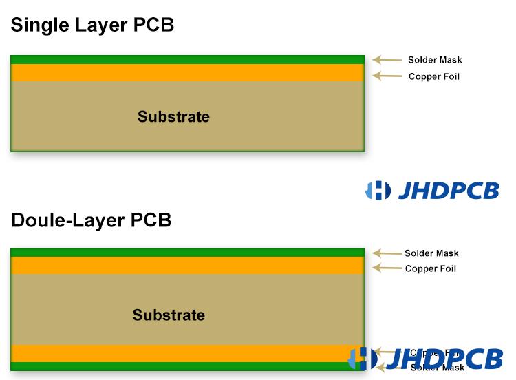
A double-sided PCB, which is also known as a dual layer pcb, double layer PCB, 2 layer PCB, double layer circuit board,has two conductive layers, which has more layers than single-layer boards, but less than multi-layer boards. Like single-sided PCBs, double-sided PCBs also have a backing layer. The difference is that they have a layer of conductive metal on both sides of the material plates.
These boards can have conductive copper and components mounted on both sides of the board, allowing traces to cross each other. This allows for higher circuit density without the need for point-to-point soldering.

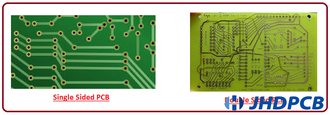
Circuits and components on one side of the board are connected to circuits and components on the other side by one of two methods:
• Through Holes: Through holes are small holes drilled in a circuit board through which wires (called leads) are passed and then soldered to the correct components.
• Surface Mount: These PCBs use leads that are soldered directly to the board. The circuit board itself becomes the routing surface for the components, allowing the circuit to take up less space.

Construction of double layer PCB.


1. Pad: The pad is just a piece of copper on which the leads of the components are mounted and bound.
2. The traces in the PCB: parts are not associated with the assistance of wires. All parts are associated with a leading material like copper.
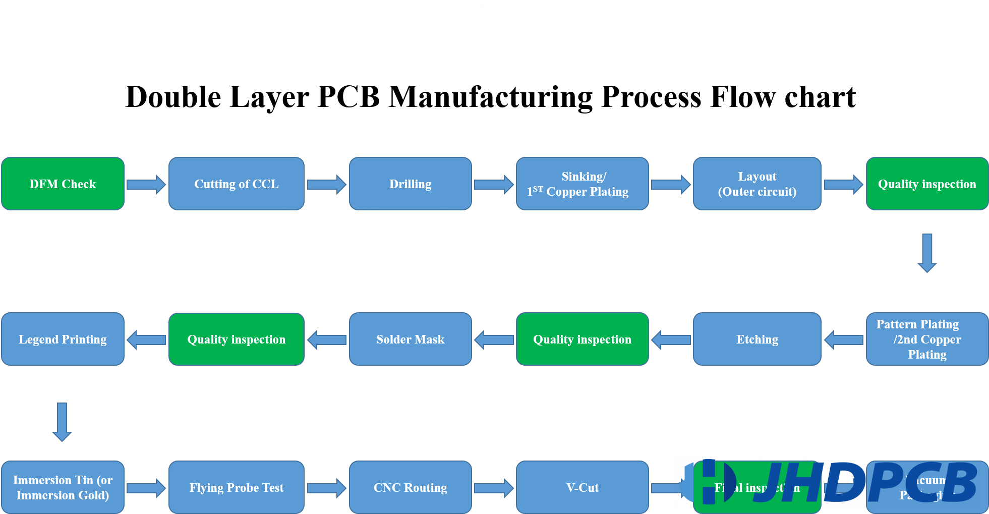
3. Number of layers: According to the purpose, cost and accessible space of the circuit, the customer can choose the number of layers of the PCB. The most straightforward in development, the easiest to plan, and the most valuable in everyday life is the single-layer PCB. Nonetheless, for large and complex circuits, dual layer pcb or multi-layer PCBs are most favored over single-layer PCBs. Currently, in a multi-layer PCB, 10-12 layers can be associated per day, and the most basic thing is to transfer between the parts of the various layers.
4. Silk layer: The silk layer is used for lines, contents or any process on the surface of the printed circuit board. In most cases, screen printing uses epoxy inks. Silk layers are available as part of the best or potential bottom layers of the PCB, as indicated by customer requirements, called Silk Top and Silk Bottom. Click to view the detailed production knowledge related to PCB silk screen printing.
5. Top and bottom layers: On the top layer of the PCB, all segments are mounted on this layer of PCB. In most cases, this layer is a shade of green. On the bottom layer of the PCB, all segments are fixed by openings, and the leads of the segments are called the bottom layer of the PCB. At a certain point, on the top or potentially bottom layer, the PCB is covered with a green shaded layer, which is called the solder veil.
6. Solder mask: There is an additional layer on top of the copper layer, which is called a solder mask. This layer is usually green, but can be any color. This insulating layer is used to prevent accidental contact of the PCB with other conductive materials.pls get more details on solder mask from “The MainType And Thickness Of Solder Mask Color And Manufacturing Process

Types of dual layer PCB.

Double-sided PCBs can be classified into different types. The types are:

  • Double-sided Rigid PCB
  • Double-sided Rigid-Flex PCB
  • Double-sided Flexible PCB
  • Double-sided Metal Core PCB
  • Double-sided High TG PCB
  • Double-sided High-Frequency PCB
  • Double-sided Heavy Copper PCB
  • Double-sided Impedance Control PCB

How are Double Sided PCBs Made?

The production of double-sided panels is more complex than single-sided panels. The main reasons are as follows:

* The top and bottom layers of copper plated/laminate must be laid out.
* The top and bottom circuits should be connected to PTH.
Especially critical is PTH, which is also the core process of double-sided production. The so-called PTH is created by coating/electroplating a layer of metal on the inner wall of the through hole to connect the printed circuit of the top and bottom layers. At present, chemical copper plating process is mainly used for PTH in China. There are two types of electroless copper plating processes:
     1) Electroless plating on thin copper first, then the entire circuit board is plated to thicken the copper layer, and finally pattern transfer is performed.
    2) Electroless plating on thick copper first, and then the pattern is directly transferred.
Both methods are widely used. However, electroless copper plating is harmful to the environment and it will be gradually replaced by more advanced technology-black hole,they are tin / palladium direct plating technology and polymer direct plating technology.
*2-layer PCB with HASL-LF/Immersion Gold surface production process:
Cutting->Drilling->Sink/First Copper Plating->Layout->Pattern Plating/Second Copper Plating->Etch->Solder Mask->Legend Print->Immersion Tin (or Immersion Gold)- >CNC wiring->V-cut (not required for some boards)->Flying probe test->Vacuum encapsulation
*Double-sided PCB gold plating production process:
Cutting->Drilling->First Copper Plating->Layout->Pattern Plating/Second Copper Plating->Gold & Nickel Plating->Etch->Solder Mask->Legend Printing->CNC Routing->V Shape Cutting->Flying Probe Test->Vacuum Packaging

Double Layer PCB Production Manufacturing process.

The benefits of double layer pcb manufacturing.

Double-sided printed circuit board (Double sided PCB) is a component that is widely used in various applications because it makes the design more flexible and the circuit more complex. Here show some advantages of 2-sided circuit boards:
The main benefit of double sided boards is that add more components on an extra layer , that effectively increases the density of the PCB. This increases design flexibility as the available space on the board increases, allowing you to place more components and have room for additional connections if needed.
Due to the larger space, double-sided boards tend to use more complex circuits. This means these boards are ideal for advanced electronics or demanding applications.
The ability to use both sides of the board effectively reduces the size of the board required. This can result in significant cost savings, making double-sided PCBs cheaper.

Single & Double-Layer PCB Production Time.

Production time: 3-5 days for sample, 7-10 days for mass production.
Quality request: The customer’s detailed requirements, size, thickness, surface, copper, surface, can it be collected by express delivery, and are there any special requirements? Are mass production required in the future? Is it long-term cooperation? These details are very important to serve customers well.

How to improve the long delivery time for1-2 layers PCB?

  1. Make more boards in stock;
  2. Arrange the full day production for urgent orders;
  3. The delivery date needs to be negotiated with the customer in. advance

Single-sided vs. double layer PCB: How to choose?

Single-sided and double-sided PCBs are differentiated based on the number of conductive layers, and they are both made of FR4 and copper foil.
Double-sided PCB can realize more complex circuit design than one layer PCB, but sometimes single-sided PCB may be more suitable for your real needs.
In terms of price, producing single-sided PCBs is more cheaper than producing double-sided PCBs.
You can also choose Single-sided or double-sided PCB according to the following applications.

What are the applications of Single & Double-layer PCBs?

1, Single PCB panels may not be as complex as other panels, but they power a variety of everyday electronics. Because of their low manufacturing cost, you can find them in mass production equipment, such as:
Lighting / Camera systems / Audio equipment / Power supplies / Calculators / Solid-state drives / Printers / Surveillance.

2, 2layers PCBs are one of the most popular PCB types because they enable manufacturers to produce more complex circuits, which is conducive to the use in higher technology applications and electronic products. Double-sided printed circuit board can be used in the application of electronic products and electronic products are very widely, such as:
Power Supply / HVAC system / Power Conversion / LED lighting / Printer / Hard disk drive / Telephone system / Vending machine / Traffic system / Car dashboard.

Two-sided PCBs can be made with a variety of custom designs, such as silver and gold finishes, high-temperature materials and solder coatings. This versatility enables them to power an almost unlimited lot of projects at a cost-effective price.

Are You Ready to Start Getting Your Quote?

If you want to do PCB prototype of 1-2 layer PCB ,including multilayers PCBs just send your Gerber files to our website:www. jhdpcb.com, we promise to delivery in 24 hours with Only $50 and free shipping!