What are PCB silkscreen and design considerations.

jhdpcb@gmail.com
Before you design or buy a printed circuit board, firstly make understand what is silkscreen of printed circuit board design? What is the function of the silk screen layer? The most common silk screen PCB printing technology. Now JHDPCB will explain it all for you.
directory
What is pcb screen printing?
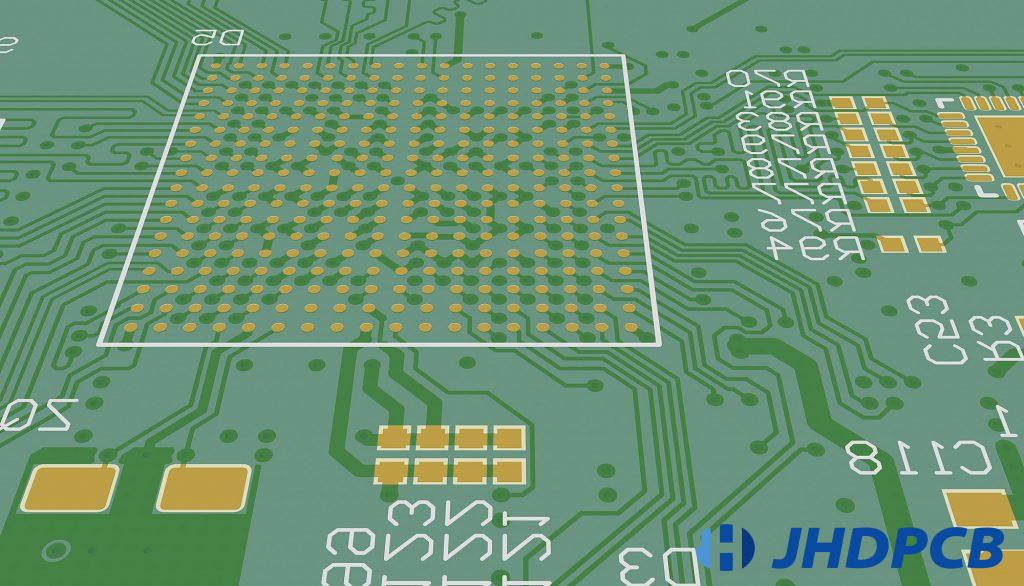
A printed circuit board (PCB) design has many different layers, and silkscreen is the topmost layer of a printed circuit board (PCB) and often occurs as the last step in the printed circuit board manufacturing process. As the pcb screen printing must be printed on the PCB surface, each PCB has two silkscreen layers layers at most,on the top side and the bottom side. In order to provide reference marks for components on PCB.
It is a non-conductive epoxy ink, which is a specially formulated ink. Its common color is white color, besides there are other pcb silkscreen colors of yellow, blue,black,red and so on. Of course, there are many other types of inks used in PCB production. This article mainly explains PCB screen printing ink.
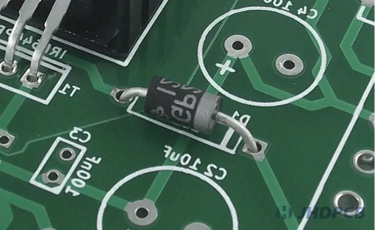
Silk screen printing is a layer of oil traces which used to spot component parts, testing points, PCB elements, warning sign, signs and tabs. Useful information to prompt PCB boards based on schematic diagrams to help manufacturers and engineers locate and identify all components during assembly. It is used to pick out elements values, PN numbers,test points, etc.
What is the function of the silk screen layer?
By default, pcb screen printing does not apply to PCB boards. Customers have to request it, and there is usually an extra cost for adding screen printing on the PCB board. Here are some important advantages to do silk screen pcb layers:
| Type | Content |
|---|---|
| Identify Test Points | It helps technicians and engineers to place testing points on a print circuit board. That way they know where to take measurements and help when troubleshooting. Check out what’s on PCB testing. |
| Component Outline | It can be used to outline where the component needs to be placed on the board so that the user does not forget to place the component on the board. |
| Warning signs | Silk screen covering also simplify the use of warning signs, which are often used to specify higher parameter values such as current, power, and voltage. |
| Reference Metrics | It can be used to indicate the value of resistors, inductors, and other component parts. Reduce the possibility of placing the wrong components on the PCB board. |
| Polarity Indication | Used to identify component type and polarity direction. Define a unique identification number for each board; |
| Unique Identification Number | Define a unique identification number for each board, It is easy to identify in the later assembly process. Avoid the wrong assembly. |
| Part Number | The component number used in PCB assembly, which is convenient for later inspection and repair of the printed circuit board. |
| Version Number | Marks the production revision of the PCB for this batch. |
| Datecode | Marks the production date of this batch of PCBs. |
Three main process methods of silk screen printing.
The following are the most common PCB silk screen technology processes and processes on PCB:
- Manual Silk Screen PCB: This process can be used when the line width is greater than 7mm and the registration tolerance is 5mm. For this method, you will need pcb silkscreen minimum text size and trace template made of nylon. The oil is printed onto the plate through the stencil. Next step,make the PCB board baked in a curing oven and let it to besolidification.
- Liquid Photo Imaging (LPI): This procedure supplied greater correctness and legibility than manual screen printing. Using this method when the trace width is greater than 4 mil. Liquid photo imaging is very similar to the process of applying solder mask. In this case, a liquid photoimageable epoxy was applied to the laminate and then exposed to UV light. After that, the PCB board is developed and cured.
- Direct Legend Printing (DLP): This is the most correct way to add PCB silk screen, but it is very high-priced. In such pcb silkscreen process, using an inkjet projector with acrylic pcb silkscreen ink, which have relevance to the original print circuit board from the CAD data. The pcb silkscreen acrylic inks is solid with UV light during printing. It should be noted that acrylic inks will not cure on boards with a silver finish.
How to design custom pcb silkscreen?
When start to design the PCB layout. In-design component reference designator codes change as they are attached to components. Such as: move, rotate. On this condition editing the silk screen pcb is required. There are also procedure in which you can design silk screen pcb and code your own assembly specified reference by using with the relevant component locations. In these programs, you only need to pay attention to the following points, while paying attention to assigning different reference codes to each component.
Orientation/Overlap:
Edit text orientation for component reference designators, part types, etc. so that all have the same orientation, and if possible set top and bottom, which means pcb silk screen are easier to read.
Check and troubleshoot overlapping pcb silkscreen text size issues before rotating text and adjusting component reference indicator markers. Avoid identifying confusion.
Additional markup:
Adding additional silkscreen markings may help identify the orientation and polarity of components on the board. For components like bulk capacitors or other components with a specific polarity, this reduces the chance of misorientation of components during PCB board assembly, helping production run smoothly.
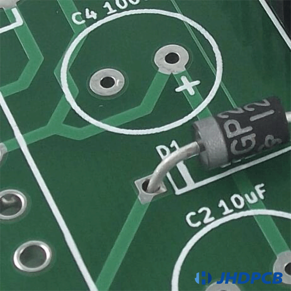
Pin 1 of the IC is usually indicated by a dot ( . ). For diodes and LEDs, “(use + or -)”, (C) for cathode and (A) for anode. For capacitors, the half-shaded circle represents the negative pole and “+” represents the positive pole.
Usually we do a rough check of the indicator marks before PCB fabrication to avoid them overlapping and possibly affecting the circuit:
- Check that the component relevant designator symbols placed overlapping the pads. To avoid being covered during manufacturing, component reference marks need to be used as a reference during PCB assembly and troubleshooting. This requires moving these markers to the open space next to the corresponding components.
- Check mark safe location. Try to avoid covering vias, pads, and solder tracks. Avoid affecting the stability of the PCB while ensuring the identification of the post-assembly process. If there is extra area, it is best to locate it near the hole.
The free PCB file inspection provided by JHD has helped many customers to solve unnecessary troubles.
Screen printing layer design considerations:
- Single-sided printing. When designing the pcb silk screen, it is guaranteed that the identification will not be affected. Can screen printing be limited to only one side. Thereby effectively reducing costs.
- Use standard colors and ensure identification. Using standard colors and larger shaped markers It makes pcb silk screen lower-cost and simpler to read. Standard colors are usually more affordable than special colors.
- The recognized characters are unified into the system font. Uniform system fonts can recognize characters on all systems in one pass.
- Keep a safe distance. Distances are measured to allow for common typographical errors on the board to a tolerance of a few mils. You can reduce the possibility of problems caused by machine printing errors.
What Information Does PCB Silkscreen Provide?
As mentioned earlier,PCB silkscreening provides a lot of information. In addition to warning labels and date codes,pcb silkscreen size,pcb silkscreen symbols,other important information highlighted by silkscreening are:
- Test points;
- Identification numbers;
- Polarity indicators;
- Components;
- PCB and PCBA part numbers;
- Company logos;
- Date codes;
- Warning and other symbols;
- Manufacturer marks;
- Reference indicators;
- Pin indicators;
- Component outlines;
Understand PCB screen printing cost.
Due to the fixed cost characteristics, the cost of PCB screen printing is placed in the first place of non recurring tools in the PCB design process. PCB screen printing process accounts for about 15% of the total cost from PCB manufacturing cost.
- The minimum text size design of PCB screen printing refers to the change of character width, height, PCB screen printing thickness, spacing and character position. Art fees are usually not charged separately.
- The cost of PCB screen printing ink depends on the screen printing method used. Acrylic ink is used for the DLP method of legend printing, while other methods use epoxy ink.
- The cost of PCB screen printing ink decided by specific features, such as curing procedure, adhesion,substrate compatibility, and immunity to acid / alkali treatment.
- PCB screen printing color is also a decisive cost factor. The cost of white ink silkscreen is lower than that of other color inks. By optimizing the cost of PCB screen printing through the selection of PCB screen printing materials, the total cost of PCB can be reduced by about 5%.
- The screen printing method that used also has an effect on the total cost. The cost of LPI for liquid photo imaging and DLP for direct legend printing is higher than that of manual screen printing because of the high capital cost of setup.
- Another important factor to consider in the cost calculation of screen printing is whether you want to print legends on both sides or just on one side. In the case of both parties, the cost will rise.
How to remove the silk screen on the printed circuit board?
If the ink is not cured removing PCB screen printing ink is the same as removing solder paste,. However, if the ink solidifies, the best way is to try to chemically dissolve and remove PCB screen printing ink.This would be difficult, but not impossible to do, if the PCB screen printing ink was epoxy-based. I hope this is not something you need to do regularly. There are some powerful but safe immersion cleaners with high solubility parameters, such as immersion cleaners based on orange terpene cleaners (citraflor eg-3 or bioct sc-10) and combined with a small amount of other solvents. These solvent mixtures are particularly effective and can be safely used in CCA, connectors, and metal parts and assemblies. They are hydrocarbons with a flash point of more than 100 degrees Fahrenheit. They do not need heating and do not produce waste water. If you don’t want to use chemical methods for cleaning, you can try “pencil eraser” There are specific types of cleaning pads, and you should consult your electronic assembly dealer for samples. These will almost wear the surface of the mat or other parts of the assembly and physically remove the ink.
PCB silk screen printing statements and precise requirements.
- All assembly parts, installing holes and positioning holes have relevant silk screen marks.
- All polar devices are oriented in the same direction and are well identifiable.
- Silkscreen letters abide by the basis of left to right and bottom to top.
- In order to guarantee the trustworthy quality of the PCB, it should be ensured that there is no silk screen on the device pads and tin-lined tin tracks.
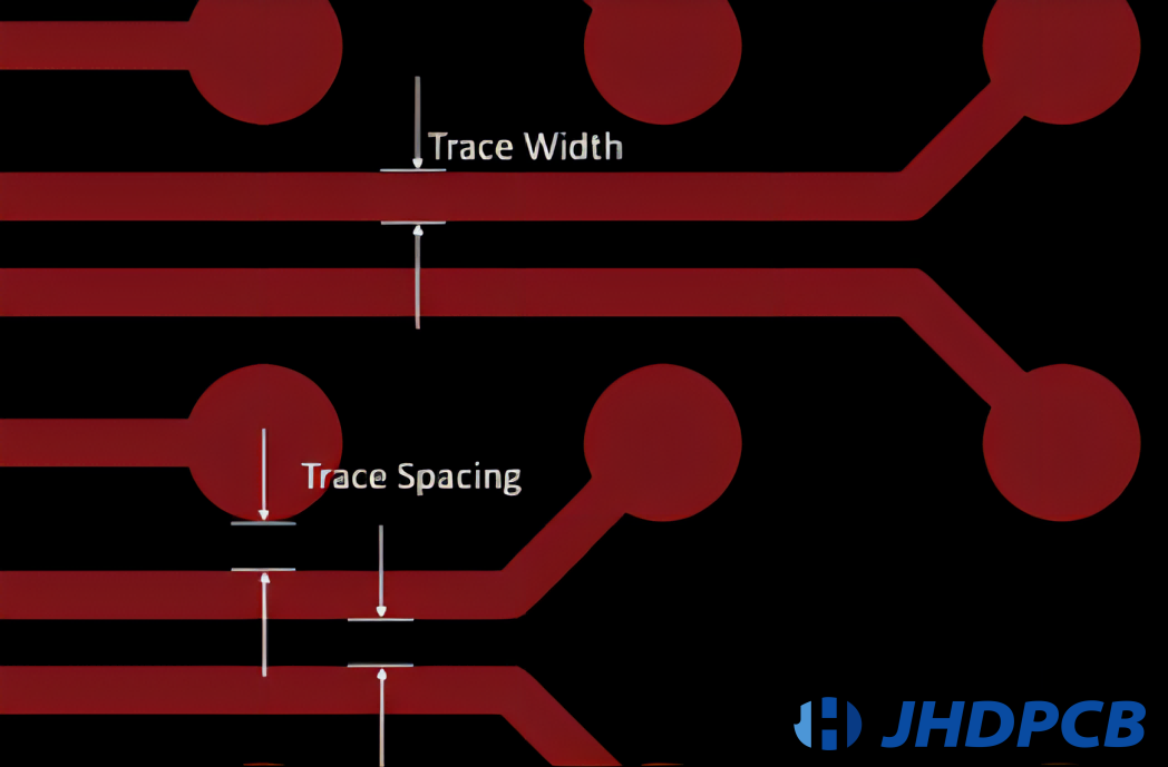
- The silk screen cannot be printed on the via holes or pads, in order to avoid causing part of the silk screen to be missed when the solder mask is opened, which will make effect on the identification. The silkscreen spacing is greater than 5mil.
- The barcode position on the PCB board should be easily scanned.
- The screen printing position of the finished board information such as the name of the PCB board, date, version number, etc., should be clear.
- Something identifies of the components on the PCB must match the identifier in the BOM list.
I believe that through the above introduction of PCB screen printing, you have a certain understanding of PCB screen printing. If you have any other PCB production questions or PCBA related needs, please feel free to contact us. As China’s top five leading PCB manufacturers, we will use our advantages and professionalism to solve your doubts.