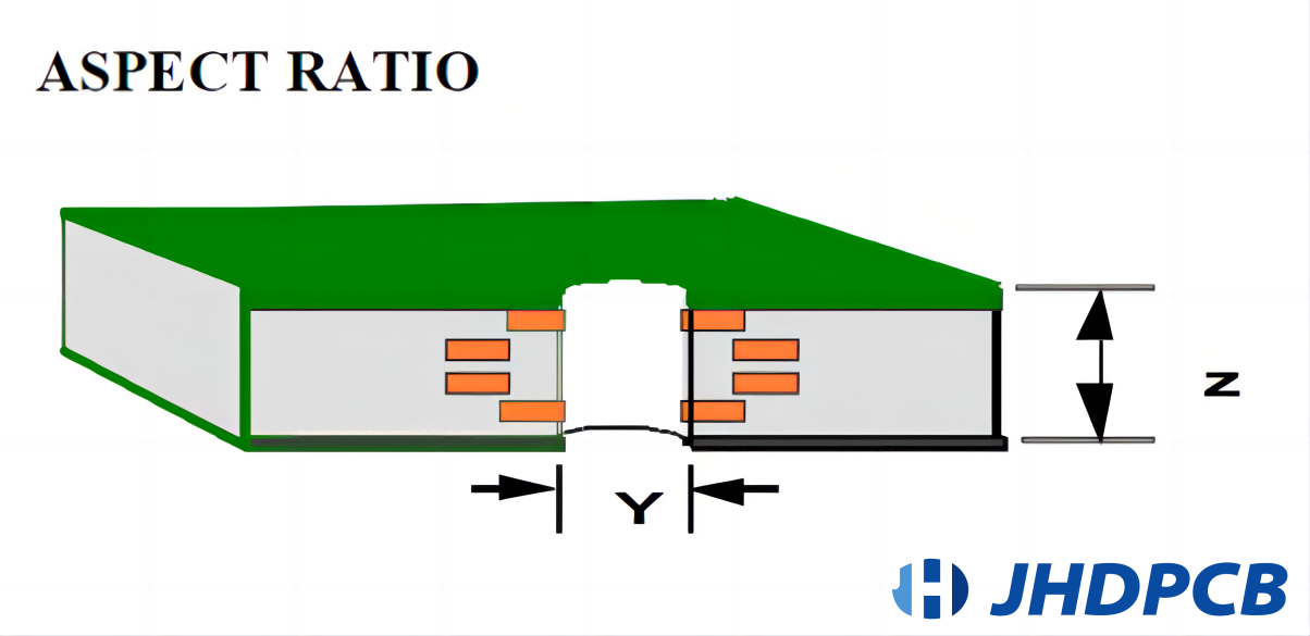
ENIG VS HASL in PCB Fabrication

ENIG VS HASL in PCB Fabrication

directory

Surface treatment in printed circuit board production is an integral part of the fabrication procedure, indicating the process of enhancing the PCB’s surface for improved performance, longevity, and aesthetic appeal. The encompassed procedures involve electroplating, applying a coating, and buffing. Here are some frequently employed surface treatments in the fabrication of printed circuit boards:

  1. HASL (Hot Air Solder Leveling): This procedure entails submerging the printed circuit board in a reservoir of liquefied solder, followed by utilizing heated air to even out and refine the surface.
  2. ENIG (Electroless Nickel Immersion Gold): This procedure involves depositing a thin coating of electroless nickel onto the PCB surface, followed by a thin veneer of immersion gold. This finish is recognized for its longevity and oxidation resistance.
  3. OSP (Organic Solderability Preservatives): This procedure entails applying a slender layer of an organic substance to the PCB surface to shield it from oxidation and enhance its solderability.
  4. Immersion Tin: Here, the surface finish consists of overlaying the printed circuit board with a layer of tin, offering robust corrosion resistance and low contact resistance.
  5. ENEPIG (Electroless Nickel Electroless Palladium Immersion Gold): Here, the surface finish is a sophisticated variant of ENIG with enhanced corrosion resistance and an impressive shelf life.
  6. Immersion Silver: This surface finish involves covering the printed circuit board with a silver layer, akin to Immersion Tin, providing robust corrosion resistance.

The choice of surface finish hinges on the specific application’s needs, such as the nature of the components to be employed, the environment where the PCB will be utilized, and the cost evaluation. Factors to take into account include solderability, expense, dependability, processability, and lead-free prerequisites, among others. HASL and ENIG are prevalent surface finishes known for their excellent solderability.

Occasionally, if the PCB is to be used in a lead-free context, then the surface finish ought to be in compliance with RoHS (Restrictions on Hazardous Substances) and WEEE (Waste from Electrical and Electronic Equipment) regulations. 

What are ENIG and HASL Surface Finish?

HASL:

PCB with HASL

  • Definition:
    Hot Air Solder Leveling, commonly known as HASL, is a surface finishing technique widely employed in the printed circuit board (PCB) industry. It provides PCBs with a reliable solder joint and an extended shelf life. Hot air solder leveling enhances the effectiveness of soldering components onto the PCB. Initially, the HASL finish is applied to improve solderability and cover exposed copper circuitry.
  • HASL Finish:
    HASL has been a prominent surface finish option in the industry for several decades, offering advantages such as cost-effectiveness, availability, and repairability. As mentioned earlier, HASL provides excellent solderability and ensures a prolonged shelf life for PCBs. During the HASL process, the exposed copper surfaces on the PCB are coated by immersing the board in a container filled with molten solder.
    Following this step, excess solder is fully removed, and the PCB is leveled by passing it through a hot air knife. It is crucial to ensure complete coverage of the entire PCB with solder; otherwise, the copper may oxidize and deteriorate, rendering the circuit board unusable.The presence of copper finishes on the PCB creates a robust interface between the board and its components, thereby facilitating reliable functionality and performance. HASL remains a popular and effective surface finish choice in the PCB industry.

ENIG

ENIG's structure

  • Definition:
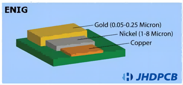
    ENIG, standing for Electroless Nickel Immersion Gold, is a commonly employed surface finish in the printed circuit board (PCB) sector. It consists of a two-layer metallic coating, with a layer of electroless nickel plating covered by a thin layer of immersion gold. ENIG has garnered favor due to its adaptability across diverse component assembly procedures.
    ENIG is named after the two main materials used in the finish. Electroless nickel plating is a chemical procedure that accrues a layer of nickel onto the PCB’s surface. This nickel layer serves as a shield between the copper and the immersion gold layer, thwarting oxidation and assuring solid solderability. The immersion gold layer is a thin coating of gold that provides a protective and solderable surface for component attachment.
  • ENIG Finish:
    The ENIG finish involves a two-layer metallic coating applied to the PCB. The electroless nickel plating serves multiple purposes. Firstly, it provides a smooth and uniform surface, enhancing the solderability of the PCB. Secondly, it acts as a diffusion barrier, preventing the migration of copper atoms into the gold layer. Finally, it enhances the bonding of the immersion gold layer.
    The immersion gold layer, renowned for its superior conductivity and corrosion resistance, holds a crucial position in the ENIG finish. It ensures reliable solder joints and protects the underlying nickel layer from oxidation during storage and assembly processes. The immersion gold layer’s thickness is usually quite slender, ranging from 0.05 to 0.2 micrometers.
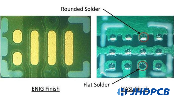
    ENIG offers several advantages that contribute to its widespread use. It is compatible with lead-free assembly processes, making it environmentally friendly. It is suitable for PCBs with plated through holes (PTH) and fine-pitch components. The ENIG finish provides a flat and uniform surface, making it suitable for wire bonding and flip-chip applications. Additionally, ENIG has a long shelf life, ensuring the reliability of PCBs even after extended storage periods.In conclusion, ENIG is a popular surface finish in the PCB industry due to its versatility, excellent solderability, corrosion resistance, and compatibility with various assembly processes. Its two-layer metallic coating, consisting of electroless nickel plating and immersion gold, provides enhanced functionality and protection for electronic components.

What's the Surface Flatness of ENIG and HASL?

HASL Surface Flatness

Hot Air Solder Leveling (HASL) is a favored surface finish employed in Printed Circuit Board (PCB) fabrication owing to its capacity to furnish a fairly even surface. However, achieving perfect surface flatness using HASL can be challenging due to several factors that impact the process and the final outcome. These elements encompass:

  1. Variations in Solder Thickness:
    Throughout the HASL procedure, liquefied solder is administered to the PCB surface, succeeded by the removal of surplus using hot air blades.This process can result in uneven solder thickness, leading to variations in surface flatness across the board.The thickness of the solder layer may vary between 30 to 50 microns depending on factors such as the type of solder used, the temperature of the solder bath, and the speed at which the board is withdrawn from the bath.
  2. Solder Mask Temperature:
    The temperature of the solder mask during the HASL process is critical to achieving a smooth and even surface finish. Temperatures that are too high can cause solvent evaporation and foaming, resulting in non-uniform solder mask thickness.
  3. Solder Paste Thickness:
    The density of the solder paste employed in the PCB assembly procedure can impact the uniformity of the solder application. High viscosity solder pastes may result in uneven deposition and rough surfaces.
  4. Surface Contamination:
    Surface contamination such as dirt or oil can affect the adhesion of the solder to the PCB surface, resulting in variations in surface flatness.
  5. Board Design:
    The design of the PCB can also impact the surface flatness achieved using HASL. For example, large copper pours can absorb more solder than narrow traces, leading to variations in surface flatness.

In conclusion, while HASL remains a popular surface finish for PCBs, achieving perfect surface flatness using this method can be challenging due to several factors. However, by carefully controlling parameters such as solder mask temperature, solder paste viscosity, and surface cleanliness, it is possible to achieve a reasonably flat surface using HASL.

ENIG Surface Flatness

The Electroless Nickel Immersion Gold (ENIG) surface finish is a commonly employed technique for Printed Circuit Boards (PCBs). The ENIG process provides superior surface flatness compared to Hot Air Solder Leveling (HASL), making it a popular choice for modern PCB designs, especially those with fine-pitch components and Ball Grid Array (BGA) packages.
ENIG provides several benefits compared to HASL in relation to surface planarity:

  1. Consistent Thickness:
    The electroless nickel plating procedure guarantees a consistent and equal thickness throughout the entire board. The nickel layer typically has a thickness ranging from 3-7 microns, while the gold layer is much thinner, ranging from 0.05-0.2 microns. This level of precision results in a highly flat surface, which is crucial for the proper functioning of electronic components on the board.
  2. Superior Planarity:
    ENIG surface finish is known for its superior planarity, which is essential for fine-pitch components and BGA packages. The thin gold layer provides an ultra-flat surface, which helps ensure a reliable electrical connection between the component and the board. This level of planarity is not possible with other surface finishes like HASL.
  3. Solderability:
    The immersion gold layer in the ENIG finish is highly solderable, ensuring reliable solder joints during assembly. Due to its excellent surface flatness and uniform thickness, the ENIG finish also enables tighter control over the solder joint formation, resulting in a more robust and reliable connection.

In summary,The ENIG vs HASL finish debate is often discussed in the context of surface finishes for PCBs. The ENIG surface finish serves as an excellent alternative to HASL, providing superior surface flatness and planarity. When comparing the enig vs hasl finish options, ENIG offers several advantages over HASL. These include uniform thickness, exceptional solderability, and improved reliability, making it a popular choice for modern PCB designs that require high-performance electronic components. Therefore, in the enig vs hasl finish comparison, ENIG emerges as the preferred option for manufacturers seeking a surface finish that delivers superior performance and reliability.

Here is a table comparing the different characteristics of HASL and ENIG:

Parameter HASL ENIG
Surface Flatness 2-15µm 0.05-0.1µm
Coating Thickness 1-40µm 0.05-0.1µm
Surface Finish Matte/Shiny Matte/Shiny
Solderability Good Excellent
Corrosion Resistance Moderate High
Lead-Free Compatibility Good Compatibility Excellent
Cost Low High
Reliability Moderate High

What about the Durability and Lifespan of ENIG vs HASL?

Certainly, here are some additional points to further expand on the durability and lifespan of ENIG vs HASL in PCB manufacturing:

Durability:

  • The gold coating of ENIG usually consists of a slim layer of nickel, succeeded by a layer of immersion gold. This unique combination provides excellent hardness, wear-resistance, and corrosion-resistance compared to HASL’s tin-lead coating.
  • The nickel layer in ENIG acts as a diffusion barrier that prevents the gold layer from diffusing into the copper substrate, ensuring long-term adhesion and preventing soldering issues.
  • The gold layer in ENIG provides excellent electrical conductivity and solderability, making it an ideal surface finish for fine-pitched components and high-frequency applications where signal integrity is critical.
  • In contrast, HASL’s tin-lead coating tends to be softer and more prone to whisker growth, which can cause electrical shorts and other reliability issues.

Lifespan:

  • ENIG’s durability and lifespan make it a preferred choice for applications with long-term reliability requirements, such as aerospace, defense, medical, and automotive electronics.
  • ENIG has a significantly longer shelf life than HASL, which means it can remain functional for a longer time even without being used. This is due to the gold layer’s resistance to oxidation and corrosion.
  • ENIG’s long-term reliability ensures consistent performance over a wide range of operating conditions, making it a popular choice for a variety of industries.

In summary, ENIG’s unique composition and properties make it a superior choice for applications requiring durability and a long lifespan. Its resistance to corrosion and wear, excellent adhesion, electrical conductivity, and solderability make it ideal for high-reliability applications where performance and reliability are critical. Overall, while ENIG may be more expensive than HASL, its superior quality and reliability make it a worthwhile investment for many applications.

HASL vs ENIG: Advantages and Disadvantages

pcb ENIG vs HASL


Advantages of HASL Surface Finish

  1. Simplicity of Application:
    HASL is a well-established and traditional surface finish process. It doesn’t require complex procedures or highly specialized equipment. The straightforward process involves immersing the printed circuit board (PCB) in a container of molten solder, then using a hot air knife to even out any excess solder. This simplicity makes it easy to apply even in smaller-scale manufacturing setups.
  2. Widespread Availability:
    As one of the most affordable surface finishes, HASL is a staple in virtually every PCB manufacturing facility. This widespread availability means that manufacturers can easily source the materials needed for this process, thereby reducing lead times and ensuring a steady supply chain.
  3. Excellent Wettability:
    Leaded HASL is known for its superb wettability. This is a critical factor in electronics manufacturing because it ensures a strong and long-lasting bond between the PCB and its components. Excellent wettability results in dependable connections, which can notably improve the efficiency and durability of the electronic equipment.
  4. Ease of Reworking:
    The primary component in HASL is solder, which can be easily reworked. This implies that in case any complications arise during the production process, adjustments can be made without substantial difficulty or cost. The ability to resolder while maintaining high-quality connections and a bright, clean surface is a substantial advantage, particularly in high-volume production lines.
  5. Affordability:
    HASL is a cost-effective option in comparison to alternative surface finishes such as Electroless Nickel Immersion Gold (ENIG) and Immersion Silver. Its cost-effectiveness is a key reason why it’s the preferred choice for a wide array of household and commercial electronic products.
  6. Established Dependability:
    Due to its extensive usage over many decades, HASL has a well-documented history of proven reliability. Manufacturers and consumers alike trust this surface finish to deliver consistent performance, making it a go-to choice for many electronic products.
  7. Visual Inspection:
    Lastly, the bright surface produced by HASL makes it easier to visually inspect the PCB for defects. This can be a significant advantage in quality control, allowing for easy detection and correction of any potential issues before the product reaches the consumer.

In conclusion, the combination of simplicity, cost-effectiveness, reliability, and excellent performance characteristics makes HASL a popular choice for PCB surface finishing.

Disadvantages of HASL Surface Finish

  1. Thickness:
    Compared to other surface finishes like Electroless Nickel Immersion Gold (ENIG) and Immersion Silver, HASL tends to result in a thicker layer. This could potentially result in irregular surfaces, affecting the general functionality and dependability of the PCB.
  2. Not Ideal for Surface-Mount Devices (SMD):
    The thickness of the HASL layer can create challenges when working with smaller Surface-Mount Devices (SMD). The excess solder might cause inconsistencies and unreliability in the solder joints of these tiny components, affecting the overall functionality of the device.
  3. Increased Risk of Solder Bridges:
    The application process of HASL, which involves immersing the entire PCB into molten solder, can lead to the formation of solder bridges, especially in closely placed pads. These solder bridges can result in electrical connections, causing short circuits and potentially resulting in malfunctions within the device. Therefore, a thorough visual inspection is required after the HASL process to ensure the integrity of the board.
  4. High-Temperature Process:
    The HASL process involves high temperatures, which can potentially cause damage to heat-sensitive components or warp the PCB itself. This is particularly a concern for boards with a high component density or those using materials that are more susceptible to heat.
  5. Strict Parameters:
    HASL has certain stringent parameters, particularly regarding the thickness of the circuit boards. Boards that are too thin or too thick may not be suitable for the HASL finish. This could potentially limit its use in applications requiring customized board thickness. In such instances, it is recommended to seek guidance from the manufacturer.
  6. Line Binding Limitations:
    HASL is not an ideal choice for line binding or fine-pitch applications. The uneven surfaces that can result from the HASL process might cause issues when trying to maintain consistent line widths, potentially affecting the performance of the device.
  7. Lead Concerns:
    Traditional HASL uses lead, which poses environmental and health concerns. While lead-free HASL options are available, they come with their own set of challenges, including a higher melting point, which can further enhance the risk of damaging heat-sensitive components.

In conclusion, while HASL is a popular choice due to its cost-effectiveness and widespread availability, these potential drawbacks need to be carefully considered when selecting the most suitable surface finish for a particular application. To guarantee maximum efficiency and dependability, it is crucial to weigh the advantages and disadvantages of HASL against the particular needs of the PCB.

Advantages of ENIG Surface Finish

  1. Availability:
    ENIG, a surface finish involving immersion gold over electroless nickel, is in high demand in the electronics industry. As such, it is generally readily available. However, it’s always a good idea to confirm with your specific manufacturer whether they offer this type of finish, considering its premium nature.
  2. Durability and Corrosion Resistance:
    One of the key advantages of ENIG is its exceptional durability. The immersion gold layer applied over the nickel plating acts as a protective shield, safeguarding the underlying copper from corrosion and adverse environmental conditions.. This significantly increases the shelf life of the PCB, making ENIG a suitable choice for applications requiring longevity.
  3. Superior Solderability:
    ENIG is renowned for its excellent solderability. It provides better wettability and a more even surface compared to HASL, leading to stronger and more reliable joints between the components and the PCB. This is especially advantageous in applications that require fine-pitch, where accuracy and dependability are of utmost importance.
  4. Non-Toxic Surface Coating:
    Unlike HASL, ENIG is a surface coating that does not contain lead. As a result, it adheres to the regulations outlined in the Waste Electrical and Electronic Equipment Directive (WEEE) and Restriction of Hazardous Substances Directive (RoHS), which require the use of electronic products free from hazardous substances such as lead. This is a significant advantage in terms of environmental sustainability and safety.
  5. Enhanced Electrical and Thermal Conductivity:
    Thanks to the gold layer, ENIG offers superior electrical and thermal conductivity compared to HASL and immersion silver. This can significantly improve the performance of the electronic device, especially in applications that require efficient heat dissipation or high-speed signal transmission.
  6. Flat Surface:
    ENIG provides a flat surface, which is critical for surface mount technologies (SMT) and fine-pitch components. This flatness ensures that components can be accurately placed and reliably soldered, which is essential for the high-density interconnects (HDI) often used in modern elect
  7. Long Shelf Life:
    The protective properties of the gold layer in ENIG contribute to a longer shelf life for the finished PCBs. This is especially advantageous for manufacturers who require long-term storage of PCBs prior to assembly.

In summary, while ENIG may be more expensive than other finishes like HASL, its advantages in terms of durability, solderability, electrical and thermal conductivity, and compliance with environmental regulations make it an attractive choice for many applications.

Disadvantages of ENIG Surface Finish

  1. Cost:
    The primary drawback of ENIG is its expense. The inclusion of gold in its formulation makes it more expensive than other surface finishes like HASL. However, the superior properties it offers, such as excellent solderability, corrosion resistance, and environmental compliance, often justify the higher cost, particularly for high-performance or long-life applications.
  2. Gold Wire Bonding Issues:
    ENIG is a delicate surface finish that can be susceptible to elevated temperatures during the soldering procedure. If not handled carefully, this can lead to issues with gold wire bonding, making it challenging to pass quality checks. Therefore, careful process control is necessary when using ENIG to avoid these potential issues.
  3. Reworking Difficulties:
    The thin gold layer over nickel in ENIG can make resoldering challenging. If mishandled, it can result in surface imperfections. During hand-soldering, the melting and suction of solidified solder can potentially remove the gold layer, leading to a need for rework. This is a significant consideration for manufacturers, particularly in high-volume production lines where rework can add substantial costs and delays.
  4. Signal Loss:
    Nickel, which forms the base layer in the ENIG finish, has a high electrical resistivity. This can potentially cause signal loss at higher frequencies, impacting the performance of the device. This is particularly a concern for high-frequency or high-speed applications, where signal integrity is crucial.
  5. Risk of Black Pad Syndrome:
    One of the known issues with ENIG is the risk of “black pad syndrome,” a defect that causes a brittle intermetallic layer to form, leading to poor solder joint integrity. This is an infrequent yet significant concern that can affect the dependability of the final product.
  6. Not Ideal for Wire Bonding:
    While ENIG provides a flat and smooth surface ideal for surface mount technologies, it is generally not the best choice for wire bonding applications due to the potential issues with gold wire bonding mentioned above.

In conclusion, although ENIG presents numerous benefits, it is crucial to thoroughly evaluate these potential drawbacks.It’s important to balance the benefits and disadvantages of ENIG against the specific requirements of the PCB and the application to ensure the best performance and reliability.

Advantages HASL ENIG
Availability Widely available due to its popularity and cost-effectiveness. Generally available, but it’s better to confirm with the specific manufacturer.
Durability Good, but can be affected by environmental factors. Excellent, with the gold layer providing protection against corrosion and harsh conditions.
Solderability Good, with leaded HASL providing excellent wettability. Superior, with better wettability and a more even surface.
Lead-Free Option Both leaded and lead-free options are available. Naturally lead-free, complying with environmental regulations.
Electrical Conductivity Good, but can be affected by the thickness of the solder layer. Superior, due to the gold layer.
Cost More cost-effective, making it a popular choice for a wide array of applications. Costlier because of the incorporation of gold.
DisadvantagesHASLENIG
ThicknessTends to be thicker, which can cause issues with smaller SMD components.Provides a flat surface, ideal for SMT and fine-pitch components.
High-Temperature ProcessThe process involves high temperatures, which can potentially damage heat-sensitive components.Sensitive to high temperatures during soldering, which can lead to bonding issues.
ReworkingEasier due to the solder component, but quality needs to be maintained.More demanding due to the presence of a thin layer of gold over nickel.
Signal LossNot typically an issue unless the solder layer is too thick.Can potentially cause signal loss at higher frequencies due to the nickel layer.
Environmental ConcernsTraditional HASL uses lead, which poses environmental and health concerns.Naturally lead-free, complying with environmental regulations.
Suitability for Fine-Pitch ApplicationsNot ideal due to the potential for uneven surfaces.Highly desirable due to its flat and smooth surface.

This table provides a general comparison, but the choice between HASL and ENIG will depend on the specific requirements of the PCB and the application

When should we use ENIG Technology?

Use ENIG Technology

Absolutely, Electroless Nickel Immersion Gold (ENIG) is a popular surface finish technology for PCBs due to its numerous advantages. Here are some scenarios where you might prefer to use ENIG technology:

  • Long Shelf Life: If your application requires PCBs to be stored for extended periods before assembly, ENIG is an excellent choice. The protective gold layer prevents oxidation and corrosion, extending the shelf life of the PCBs.
  • Hassle-Free Solderability: ENIG provides superior solderability, with better wettability and a more even surface compared to other finishes like HASL. This leads to stronger and more reliable joints between the components and the PCB, which is particularly beneficial in applications requiring high reliability.
  • High Strength and Anti-Friction: The gold layer in ENIG provides high mechanical strength and anti-friction properties. This makes ENIG PCBs suitable for applications with mechanical stress or where wear resistance is required, such as connectors and keypads.
  • Low Contact Resistance: The gold layer in ENIG also offers low contact resistance, which is crucial for high-speed or high-frequency applications.This can greatly enhance the operational efficiency of the electronic device.
  • Excellent Plating Around the Holes: ENIG provides excellent plating around the holes in the PCB, ensuring reliable connections and enhancing the overall performance of the PCB.
  • Environmental Compliance: ENIG is a lead-free surface finish, making it compliant with environmental regulations like the Waste Electrical and Electronic Equipment Directive (WEEE) and Restriction of Hazardous Substances Directive (RoHS). If environmental sustainability is a concern, ENIG is a good choice.
  • Fine-Pitch Applications: The flat and smooth surface provided by ENIG is ideal for surface mount technologies (SMT) and fine-pitch components. This is critical for high-density interconnects (HDI) often used in modern electronics.
  • High-Temperature Applications: The high melting point of gold makes ENIG suitable for applications that require high operating temperatures.

In conclusion, while ENIG may be more expensive than other finishes like HASL, its advantages in terms of durability, solderability, electrical conductivity, and environmental compliance make it an attractive choice for many applications. As always, the specific requirements of the PCB and the application should be considered when choosing a surface finish.

When should we use HASL Technology?

use HASL Technology

Hot Air Solder Leveling (HASL) is indeed a popular surface finish technology for PCBs due to its cost-effectiveness, availability, and ease of use. Here are some scenarios where you might prefer to use HASL technology:

  • Cost-Effectiveness: If you are working with a tight budget, HASL is an excellent choice. It’s one of the most cost-effective surface finish technologies available, making it ideal for applications where cost is a significant factor.
  • Availability: HASL is one of the most widely used surface finishes, and as such, it’s readily available from most PCB manufacturers. This means you can often get quicker turnaround times with HASL compared to other finishes.
  • Ease of Use: The HASL process is relatively straightforward and well-understood, making it easy to implement and manage. This can lead to fewer production issues and higher production yields.
  • Good Solderability: HASL offers excellent solderability, guaranteeing dependable connections between the components and the PCB. This is particularly beneficial in applications where good solder joints are crucial.
  • Reworkability: HASL PCBs are relatively easy to rework compared to other finishes like ENIG. The solder component can be melted and reflowed, making it easier to fix any production defects.
  • Durability: HASL provides a reasonably durable surface finish that can withstand normal handling and assembly processes.
  • Leaded and Lead-Free Options: Traditional HASL uses lead, but lead-free HASL options are also available for applications where environmental regulations or health concerns are a factor.

Nevertheless, it is essential to acknowledge that HASL may not be suitable for every application. For example, it’s not ideal for fine-pitch components due to the potential for uneven surfaces, and the high temperatures involved in the HASL process can potentially damage heat-sensitive components. As always, the specific requirements of the PCB and the application should be considered when choosing a surface finish.

FAQ of ENIG and HASL

It’s possible to use both ENIG and HASL on the same PCB, but it’s not common. This technique is called “mixed surface finish” or “selective plating,” and it’s used to provide different surface finishes for different parts of the PCB. However, this approach adds complexity to the manufacturing process and may require additional testing to ensure compatibility between the two surface finishes.

Using mixed surface finish on a PCB can provide several benefits, such as cost reduction, improved performance, and increased reliability. By using different surface finishes for different parts of the PCB, you can optimize the manufacturing process and reduce costs without compromising the quality of the final product. Additionally, you can improve the performance and reliability of the PCB by providing the best surface finish for each component.

Using mixed surface finish on a PCB can pose challenges including compatibility issues, additional testing, and increased complexity. The different surface finishes may not adhere well and can affect reliability. Additional testing is required to ensure specifications are met, and the manufacturing process becomes more complex, potentially leading to errors and delays.

Lead-free HASL is a surface finish technique used in PCB manufacturing that applies a layer of tin-copper alloy onto the PCB surface. It is cost-effective and environmentally friendly as it does not contain harmful lead elements, complying with regulations on hazardous substances. While it offers good solderability and corrosion resistance, it may have slightly lower flatness and durability compared to other high-end surface finish methods.

Besides lead-free HASL, other commonly used surface finish techniques in PCB manufacturing include Electroless Nickel Immersion Gold (ENIG), Immersion Tin (ISn), Organic Solderability Preservative (OSP), and Electroplated Nickel Gold (ENEPIG).

OSP surface finish is cost-effective and environmentally friendly. It provides a flat and planar surface, making it suitable for fine-pitch components. OSP also offers good solderability and thermal resistance, making it a popular choice for many PCB applications.

Immersion Tin (ISn) surface finish offers a flat and smooth surface, making it suitable for fine-pitch components. It provides good solderability and is compatible with lead-free soldering processes. However, ISn may be susceptible to oxidation over time, which can affect its solderability.

ENEPIG surface finish is commonly used for applications requiring high reliability and long shelf life. It consists of a layer of electroplated nickel, followed by a layer of immersion gold. ENEPIG provides excellent corrosion resistance, solderability, and wire bonding capabilities.

In conclusion, ENIG and HASL are two common PCB surface finishing technologies. ENIG provides better solderability, durability, and environmental compliance, making it suitable for applications that require long-term use, high reliability, low contact resistance, high strength, and friction resistance. HASL, on the other hand, is suitable for budget-constrained projects that prioritize ease of operation and reworkability, although its reliability, durability, and environmental compliance may not be as high as ENIG. The selection of the suitable surface finish technology relies on the particular demands and limitations of the project at hand.

As a professional PCB manufacturer, JHDPCB offers a wide range of services, including various surface finishing technologies such as ENIG and HASL. With advanced equipment and an experienced team, we can provide high-quality, reliable, and environmentally friendly PCB products tailored to our customers’ needs. Whether you require ENIG or HASL or any other surface finish technology, we are committed to providing you with professional support and solutions to ensure the success of your project. Please don’t hesitate to reach out to us at any time to obtain further information about our services and how we can fulfill your PCB needs.

Get a PCB Quote Now

Open high-quality PCB manufacturing services in JHDPCB

Leave a Comment