PCB Laminate bubbling

PCB Laminate bubbling questions and solutions

directory

What is PCB Laminate bubbling?

Delamination in printed circuit boards (PCBs) is a critical issue that can impact their functionality and reliability. It occurs when the layers of the PCB separate from each other, leading to visible gaps or bubbles known as blisters.

The primary cause of delamination is the exposure of the laminate on the base material to humidity. During the production process, the application of heat converts the moisture into a gas, which creates blistering and induces movement between the layers.

Printed circuit boards (PCBs) usually consist of numerous layers, and FR-4 is a frequently employed substrate material. FR-4 is a laminate material woven from fiberglass, and it is bound together by a flame-resistant epoxy resin. Delamination of pcb can occur when the heat and humidity cause the resin to detach from the fiberglass or from the foil or laminate.

The process of delamination unfolds in two distinctive steps. Initially, adhesive failure takes place as the resin starts to loosen and disintegrate, resulting in the formation of blisters. Subsequently, the boards begin to separate since they are no longer held together by the adhesive. This cumulative effect puts additional strain on the weakened adhesive as the boards shift positions, leading to further separation.

Once delamination in pcb begins, there are potential remedies available, although their success is not guaranteed. Therefore, efforts primarily focus on preventing delamination. It is crucial to address production-related issues since delamination is predominantly caused by factors during manufacturing. Implementing batch testing, employing high-quality materials, and adhering to controlled production methods are effective measures to mitigate the risk of delamination. Additionally, optimizing the design and considering environmental factors during PCB fabrication can also contribute to preventing delamination and ensuring the reliability of the boards. 

Influence of Laminate bubbling

The occurrence of delamination in printed circuit boards can have notable implications for the functionality and dependability of electronic devices. Here are some further elaborations on the impacts of delamination:

  1. Electrical performance degradation: Delamination disrupts the electrical connections between different layers of the PCB, leading to increased resistance, signal loss, and impedance variations. This can result in poor signal integrity, reduced power transfer efficiency, and compromised functionality of the circuitry.
  2. Thermal management issues: Delamination creates air gaps within the PCB, which impede effective heat dissipation. Heat generated by components cannot be efficiently conducted away, causing localized hotspots and potential overheating. Consequently, this can lead to early malfunction of components and a general decrease in the overall reliability of the system。
  3. Diminished mechanical robustness: The detachment of layers undermines the structural strength of the PCB, rendering it more vulnerable to mechanical strain and vibrations.This can lead to increased mechanical failures, such as fractures, warping, or even complete board failure under normal operating conditions or during transportation or installation.
  4. Environmental susceptibility: Delamination compromises the moisture barrier properties of the PCB, rendering it more vulnerable to environmental factors like humidity, moisture, and chemical exposure. This can accelerate corrosion, oxidation, and the formation of conductive paths between adjacent layers, leading to short circuits, leakage currents, and overall decreased reliability.
  5. Manufacturing yield and cost implications: Delamination during the production process can result in rejected PCBs, increasing manufacturing costs and reducing overall yield. Additionally, post-production delamination discovered during testing or in the field may require costly repairs or replacement of affected components.

JHDPCB stands out as a manufacturer that excels in mitigating these impacts through our expertise in various techniques, including improved material selection, optimized fabrication processes, enhanced quality control measures, and thorough reliability testing. By proactively addressing delamination risks, JHDPCB ensures the longevity, performance, and safety of electronic devices relying on our printed circuit boards. With our commitment to excellence, we have established a strong track record in delivering high-quality products that meet the industry’s highest standards.

What is the difference between delamination and measling?

difference between delamination and measling

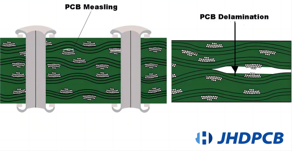
Indeed, the occurrence of delamination and measling in the domain of printed circuit boards (PCBs) is undeniably a matter of great concern. Delamination, which refers to the separation of PCB layers, can occur due to various environmental and mechanical factors. Moisture exposure, for instance, can lead to the formation of micro-cracks within the layers, ultimately causing them to separate. Similarly, temperature changes and mechanical stress can exacerbate this process, leading to the weakening of the overall structural integrity of the PCB.

On the flip side, measling is defined by the emergence of tiny cracks or distortions on the PCB surface. This type of damage is often attributed to thermal stress or mechanical shock, both of which can result from operational use or mishandling of the electronic device. As time progresses, these cracks can spread and undermine the functionality and dependability of the PCB. 

The repercussions of these types of damage are significant. In addition to affecting the electrical performance of the PCB, they can also impact the mechanical properties, such as the board’s ability to withstand vibrations and mechanical loads. Furthermore, the presence of delamination or measling can hinder the manufacturability of the PCB, making it more susceptible to failure during assembly and testing processes.

To address these issues, it is crucial to employ effective diagnostic techniques to identify the extent of the damage. Non-destructive testing methods, such as infrared thermography and acoustic microscopy, can be utilized to assess the internal structure of the PCB and detect any anomalies indicative of delamination or measling.

In terms of repair, the approach varies for each type of damage. Delamination often necessitates a comprehensive repair process involving the re-bonding of layers or even the replacement of the affected sections. Advanced techniques such as laser ablation and resin infusion may be employed to restore the integrity of the PCB. Measling, on the other hand, may be addressed through localized cleaning and reworking of the affected areas, which can help mitigate the propagation of cracks and deformations.

Delamination Measling
Definition Separation of PCB layers Small cracks or deformations on the PCB surface
Cause Moisture exposure, temperature changes, mechanical stress Thermal stress, mechanical shock
Type of Damage Physical detachment of PCB layers Surface-level cracks and deformations
Impact Compromises structural integrity, potential electrical discontinuities Affects electrical performance and reliability
Location Occurs between PCB layers Surface of the PCB
Repair Layer re-bonding or replacement Cleaning and reworking of affected areas
Diagnostic Methods Infrared thermography, acoustic microscopy Visual inspection, microscopy

What can cause PCB laminate bubbling?

cause PCB laminate bubbling

When it comes to the issue of blistering on PCB surfaces, there are several potential causes and solutions. Moisture absorption, outgassing, causes of delamination in PCB, trapped solvents, thermal stress, production flaws, contamination, inadequate soldering or reflow processes, improper storage and handling, and material quality issues can all contribute to the formation of blisters on PCB surfaces. However, through measures such as proper storage, material selection, process control, cleanliness practices, and appropriate thermal management, these issues can be effectively prevented and addressed. In the following discussion, we will delve into each of these causes of delamination in PCB and their corresponding solutions to ensure that manufacturers like JHDPCB produce high-quality and reliable electronic devices.

One of the primary reasons behind blistering on the exteriors of PCBs is the absorption of moisture during the production process, especially when the PCB delamination temperature is exceeded. The PCB material, including the core material, partially cured sheet, and copper foil, may contain moisture. When subjected to high temperatures during soldering or assembly, any remaining moisture can evaporate, causing blisters to form on the surface.

Resolution: In order to minimize the effects of moisture absorption, it is essential to store PCB materials in a controlled environment with minimal humidity. Additionally, ensuring thorough drying of the PCB material before assembly will avert moisture-induced blistering.

Outgassing transpires when volatile compounds present in PCB materials are released during high-temperature procedures like soldering or reflow. The emitted gases can get trapped beneath the solder mask or conformal coating, resulting in the generation of air pockets.

Resolution: Employing materials with low outgassing properties and comprehensive material testing can help diminish the possibility of outgassing. Adequate curing of the solder mask and conformal coating will also prevent gas retention.

The occurrence of delamination, where individual layers within a PCB become separated, can be attributed to insufficient bonding in the manufacturing process. Delamination can lead to the formation of air pockets on the surface of the PCB.

Resolution: Ensuring appropriate handling and storage of PCB materials, as well as controlling the parameters of the lamination process, are essential steps in preventing delamination. Regular examination and testing throughout the manufacturing process will help identify and address delamination problems at an early stage.

Trapped solvents are commonly used as carriers for coating materials when applying solder mask or conformal coatings. If these solvents become trapped within the coating or between the coating and the substrate, they can lead to the creation of air pockets during curing or exposure to heat stress.

Solution: Utilizing suitable coating application methods and ensuring sufficient ventilation during the curing process will aid in averting solvent retention.

Printed circuit boards (PCBs) experience thermal strain at different points in their lifecycle, including soldering, reflow, and operation. Repetitive heat cycles cause different materials to expand and contract, leading to blistering of the PCB surface.

Resolution: Careful choice of materials that have compatible Thermal Coefficient of Expansion (TCE) and effective thermal management techniques can help mitigate the effects of thermal stress on the PCB. Additionally, designing the PCB layout in a manner that facilitates even distribution and dissipation of heat can reduce the occurrence of blistering caused by thermal stress.

Blistering can also arise from production flaws, such as insufficient cleaning during manufacturing, contamination, or improper handling of PCB materials.

Resolution: Thorough quality control protocols and frequent inspections throughout the manufacturing process can assist in detecting and correcting potential production defects that could result in blistering.

Contamination during the manufacturing process, such as dust, oils, or residues, can contribute to blistering on PCB surfaces. When contaminants are trapped between layers or under coatings, they can cause air pockets to form.

Solution: Implementing strict cleanliness measures, including proper cleaning procedures for PCB materials and manufacturing equipment, can help minimize contamination-related blistering. Using cleanroom environments and ensuring proper handling techniques will also reduce the risk of introducing contaminants.

Improper soldering or reflow processes, including insufficient preheating or cooling, uneven temperature distribution, or incorrect solder paste application, can lead to blistering on PCB surfaces.

Solution: Implementing optimized soldering and reflow profiles that adhere to industry standards, along with thorough process validation and monitoring, will help ensure proper heat transfer during assembly. Training operators on correct soldering techniques and regularly calibrating and maintaining equipment will also contribute to reducing blistering caused by inadequate processes.

Incorrect storage and handling practices, such as exposing PCBs to high humidity or extreme temperatures, mishandling during transportation, or stacking heavy objects on top of PCBs, can result in blistering due to physical stress or moisture absorption.

Solution: Establishing proper storage conditions, including temperature and humidity controls, and implementing appropriate handling guidelines, such as using protective packaging and avoiding excessive pressure or bending, will help prevent damage and blistering caused by improper storage and handling.

Substandard or inconsistent material quality, including inferior laminates, copper foils, or soldermask materials, can contribute to blistering on PCB surfaces.

Solution: Working with reputable suppliers and conducting thorough material qualification and testing can help ensure the use of high-quality and reliable materials. Regularly auditing suppliers and maintaining a robust quality assurance program will minimize the risk of material-related blistering.

By addressing these various causes and implementing the suggested solutions, manufacturers like JHDPCB can effectively mitigate blistering issues on PCB surfaces, ensuring the production of high-quality and reliable electronic devices.

The test of Measuring Delamination.

The integrity and reliability of printed circuit boards (PCBs) are crucial for the proper functioning of electronic devices. The occurrence of delamination, the separation between PCB layers, can have a substantial impact on the performance and durability of the board. To ensure the identification and evaluation of delamination, multiple testing techniques have been devised.

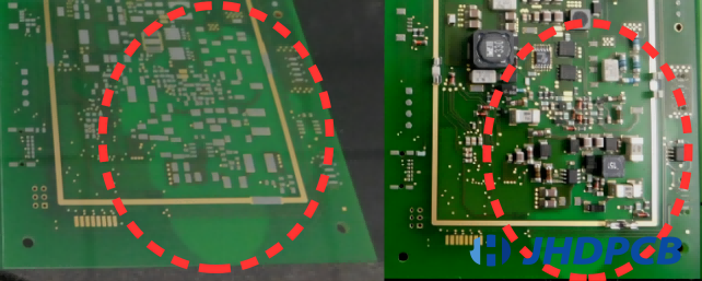
Visual examination is a basic approach for identifying delamination on PCBs. Trained inspectors examine the PCB surfaces for any visible signs of separation, blistering, or irregularities between layers. This method is often the first step in identifying potential delamination issues and can be performed quickly and cost-effectively.

Cross-section Analysis

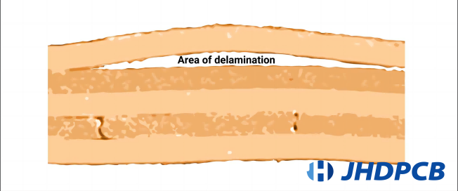
Cross-section analysis involves taking a small sample from the PCB, typically through a targeted cut, and examining it under a microscope. By analyzing the cross-section of the PCB, technicians can visually assess the integrity of the internal layers, identify any signs of delamination or separation, and evaluate the quality of interlayer bonding.
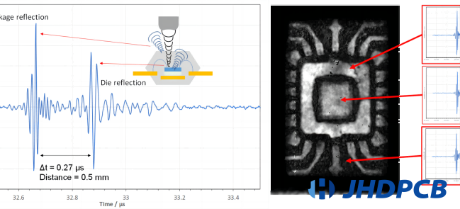
Acoustic microscopy utilizes high-frequency sound waves to probe the internal structure of the PCB. By sending ultrasonic waves into the PCB and analyzing the reflected waves, this method can detect and locate areas where delamination has occurred. It provides detailed imaging of the internal layers and is particularly effective for identifying hidden defects.

X-ray Inspection

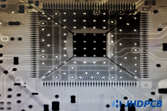
X-ray inspection involves capturing images of the internal layers of the PCB using X-ray technology. By passing X-rays through the PCB and capturing the resulting images, inspectors can visualize the internal structure and identify any voids, separations, or delamination between layers. This non-destructive method is valuable for assessing the integrity of multilayer PCBs.

TMA is a technique that measures the dimensional changes of a material in response to controlled temperature and mechanical stress. When applied to PCBs, TMA can reveal delamination by subjecting the PCB to varying temperatures and observing its expansion and contraction behavior. Changes in dimensions can indicate the presence of delamination between layers.

Scanning Acoustic Tomography (SAT)

SAT is a non-destructive testing method that uses ultrasound waves to create a three-dimensional image of the PCB. By transmitting and receiving ultrasound signals through the PCB, SAT can detect and localize areas of delamination within the structure. It provides detailed imaging and precise localization of delamination defects.

Each of these testing methods offers unique advantages and capabilities for assessing delamination in PCBs. Depending on the specific requirements, manufacturers may employ a combination of these techniques to comprehensively evaluate the integrity and reliability of their PCB assemblies.

How to fix PCB Laminate bubbling?

PCB delamination refers to the separation of layers in a printed circuit board, which can lead to electrical connectivity issues. Here are the general steps and tools commonly used for PCB laminate bubble repair:

Tools:

  • Microscope:Used for inspecting the delaminated area and for precision work.
  • Scalpel or X-Acto Knife:For carefully removing damaged areas.
  • Fine-Grit Sandpaper or Abrasive Pad: Employed to cleanse and enhance surface texture to achieve improved adhesion.
  • Isopropyl Alcohol or Acetone: For cleaning and degreasing the surfaces.
  • Soldering Iron and Solder: For reworking any damaged traces or components.
  • Epoxy Resin: To bond and fill the delaminated areas.
  • Curing Lamp or Oven: If the epoxy resin requires curing with UV light or heat.

How to Fix Bubbling Laminate

how to fix laminate bubbles

  1. Inspect the Delamination: Use a microscope to carefully inspect the delaminated area and assess the extent of the damage.
  2. Remove Damaged Areas: Use a scalpel or X-Acto knife to gently remove any delaminated or damaged sections of the PCB.
  3. Clean and Prep Surfaces: Use fine-grit sandpaper or an abrasive pad to clean and roughen the surfaces around the delaminated area. Utilize isopropyl alcohol or acetone to thoroughly cleanse the area and ensure it is devoid of contaminants.
  4. Apply Epoxy Resin: Carefully apply epoxy resin to the delaminated area, ensuring that it fills the gaps and bonds the layers together. Use a microscope for precision application.
  5. Cure the Epoxy: If necessary, cure the epoxy using a curing lamp or oven according to the manufacturer’s instructions.
  6. Rework Components: If any components or traces were damaged during the delamination, use a soldering iron to rework and repair them as needed.
  7. Inspect and Test: After the repair, inspect the area again under the microscope to ensure proper bonding and connectivity. Test the PCB for functionality and electrical continuity.

It’s important to note that PCB delamination repair can be delicate and may require advanced skills, especially when dealing with multilayer boards. If you lack expertise in PCB repair, it might be wise to consider seeking professional help.

How to prevent PCB Laminate bubbling?

The initial step in averting delamination involves comprehending its root causes. Equally vital is the prevention of delamination during PCB manufacturing, which entails the implementation of various strategies throughout the manufacturing process.

  1. Dry Manufacturing Environments:
    The primary prerequisite is that the manufacturer maintains a consistently dry production area. Prior to thermal processing, any existing oxide layer on the circuit board must remain devoid of moisture. Failure to do so will result in the conversion of moisture into gas due to heat, leading to delamination.
  2. Appropriate Baking:
    Subsequently, the boards need to undergo baking before undergoing thermal processing. The oven temperature needs to be higher than the boiling point of water, which is 100°C. Another critical aspect is the positioning within the oven. PCBs should not be stacked; instead, they should have sufficient space for movement on all sides.
  3. Utilize High-Quality Components:
    Even with adherence to proper production practices, complete certainty in preventing delamination is unattainable. Even with exact compliance with manufacturing instructions, layer separation may still occur in the boards. In addition to the previously mentioned actions, it is crucial to use high-grade materials.
    The internal layers of the board require an oxide coating, serving as a vital defense barrier against environmental hazards and thermal stress. To ensure optimal protection, this oxide coating should be uniformly applied across the printed circuit boards.
  4. Superior Solder Materials:
    Solder materials must exhibit excellent thermal conductivity (facilitating efficient heat transfer between two points) and minimal thermal resistance (preventing excessive heat absorption). Tin/silver alloy is considered the best solder due to its possession of both these qualities.
  5. Enhance Assembly Techniques:
    It is essential to refrain from exerting excessive force or pressure during the assembly of electrical devices, as such actions could inflict damage upon the board and render it susceptible to delamination.
  6. Controlled Cooling:
    After the thermal processing of PCBs, it is crucial to ensure a controlled cooling process. Fast cooling can induce thermal stress in the board, which may result in delamination. Gradual and controlled cooling helps the board to adjust to temperature changes without causing internal stresses.
  7. Proper Lamination Pressures and Times:
    During the lamination process, it is important to apply the correct pressure and ensure the appropriate duration for which the layers are pressed together. This helps in achieving optimal bonding between the layers, reducing the chances of delamination.
  8. Quality Control Measures:
    Implementing stringent quality control protocols during every stage of the manufacturing process can aid in early detection of any potential problems. This includes thorough inspection of materials, monitoring environmental conditions, and conducting regular checks during each stage of production.
  9. Adherence to Design Guidelines:
    Following design guidelines and best practices for PCB layout and construction can significantly contribute to preventing delamination. Proper consideration of factors such as material selection, layer stacking, and trace routing can help mitigate the risk of delamination.
  10. Environmental Monitoring:
    Maintaining stable environmental conditions, including temperature and humidity control, is critical for preventing moisture absorption by the PCB materials. Environmental monitoring and control systems can help ensure that the manufacturing environment remains conducive to preventing delamination.
  11. Testing and Reliability Assessment:

    Conducting comprehensive testing and reliability assessments on finished PCBs can provide valuable insights into their performance under different conditions. This can help identify any potential weaknesses that could lead to delamination and allow for necessary adjustments to be made.

Q&A of PCB Laminate bubbling

A PCB bubble etch tank is a piece of equipment used in the process of etching printed circuit boards (PCBs). It is designed to agitate the etchant solution by introducing air bubbles, which helps to maintain uniform etching and prevent uneven removal of copper from the PCB.

PCB foam, also known as gasket foam or cushioning foam, is a type of material used to provide cushioning and vibration isolation between a printed circuit board (PCB) and a mounting plate or enclosure. It is designed to absorb shocks, reduce vibration, and create a secure interface between the PCB and its surrounding components.

The foam placed between the PCB and the mounting plate in electronic enclosures serves to isolate the PCB from the external environment, dampen vibrations, and provide a stable and secure mounting surface. This helps to maintain the integrity of the PCB, reduce the impact of external shocks, and enhance the overall reliability of the electronic enclosure.

Gaps or bubbles in a printed circuit board (PCB) can lead to delamination, compromising the structural integrity and electrical performance of the board. Delamination may lead to diminished connectivity, signal attenuation, heightened electrical resistance, and potentially complete malfunction of the PCB.

The oxide layer on metallic surfaces can act as a barrier against delamination in electronic components. The oxide layer provides a protective coating that helps prevent the migration of moisture or other contaminants, reducing the risk of delamination between different layers or materials.

Using high-quality materials in the fabrication of printed circuit boards (PCBs) can help prevent delamination. High-quality PCB base materials, such as epoxy resin with good adhesive properties, provide better bonding between layers and resist delamination caused by mechanical or thermal stress.

Thermal stress can contribute to delamination in electronic components or PCBs. When exposed to rapid temperature changes or high temperatures, the different materials within the components or PCBs can expand or contract at different rates, causing stress that may lead to delamination.

Conductive anodic filamentation (CAF) is a phenomenon that can occur in PCB manufacturing processes. It involves the growth of conductive filaments between different conductive layers within a PCB, which can lead to short circuits and electrical failures.

White spots can be a visual indication of delamination in electronic components or printed circuit boards (PCBs). These spots typically occur where the layers have separated, exposing the underlying material, which may appear as white or lighter in color compared to the surrounding area.

Delamination in printed circuit boards (PCBs) occurs due to factors such as manufacturing defects, thermal and mechanical stress, moisture ingress, and ageing or degradation of materials.

To sum up, it is essential to deal with PCB lamination bubbles and delamination issues to guarantee the reliability and performance of electronic devices. By employing stringent quality control measures, conducting thorough material inspections, and adhering to best practices in lamination processes, manufacturers can mitigate the risks associated with these challenges. Additionally, ongoing research and development efforts aimed at advancing lamination technologies will play a pivotal role in minimizing the occurrence of PCB lamination bubble and delamination defects in the future. Ultimately, a steadfast commitment to quality and innovation will pave the way for robust and resilient PCBs that meet the demands of diverse applications across industries.

As an expert PCB manufacturer, JHDPCB is capable of offering all-encompassing services to tackle these concerns. We prioritize quality control and employ advanced inspection techniques to ensure that our PCBs are free from lamination bubble and delamination defects. Through our proficiency and commitment to advancement, we endeavor to furnish top-notch PCBs that fulfill the rigorous demands of our clients.

Get a PCB Quote Now

Open high-quality PCB manufacturing services in JHDPCB

Leave a Comment