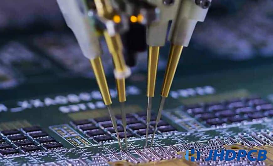

Flying probe E-testing, just as its name implies, uses a “flying” test probe, e.g. the test probe moves from this test point to other test point on the basis of instructions given by a specific software program written for the tested PCB. No custom fixtures are required, so if used on an assembled PCB, it can also be called fixtureless in-circuit testing. Therefore, it is high cost performance for prototypes and low-medium quantities production.
Originally, the flying probe tester was only used for prototyping PCB testing, but now it has become the regular for bare board testing (including testing the short circuit and open circuit between the copper conductor features on the bare PCB). The main different electrical parameters of resistance between the two nodes.
However, the development of FPT has been slow to measure capacitance and inductance in addition to resistance. This makes them suitable for PCB assemblies as well. Not only that, but there are several reasons to finally adopt them to test filler panels:
First, as mentioned earlier, they are more cost-effective for small batch production.
Second, they don’t present as many accessibility issues as ICT testers using pogo pins; FPT probe points are smaller compared to pogo pins and are able to reach much smaller test points than pogo pins many pads. For ICT tests, test points are specially designed, which is rarely required for FPT tests.
Third, testing content are easy to finished flexiblely as the movement of the FPT probes which controlled by a software program that can be easily transformed. Also, it is much easier to adjust for changes in probe landing position through software changes.
Fourth, since flying probes can directly access component pins through automatic probing without the need to build test points specifically, it provides better test coverage compared to traditional ICT testing.
If you want to study more about other types of inspections such as AOI, ICT and son on, pls read our post on PCB Assembly Inspection Report Formats. It includes an overview of each inspection test, process parameters and condition requirements.
The FPT is equipped with a camera for checking component polarity. They are becoming a more popular test way, especially with the ever-increasing miniaturization of electronics. 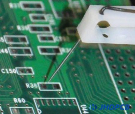
To be able to test board assemblies in FPT, we need to create an FPT program for testing. We usually create such program off line on computer,just like pick an SMT program with an SMT programming application.
Phase difference measuring device:
A phase difference measuring device (PDM) transmits a high frequency signal between one end point of the reference line and the signal line section, and measures the phase of the signal at the other end, thereby estimating its phase difference. This will reduce isolation testing within the network.
High Pressure Stress Test (HVS):
High-voltage stress testing is performed for high-resistance insulation defects not detected by PDM. We perform HVS by applying high-voltage pulses between signal lines to detect high-resistance defects.So as to do it with fast time.
Micro short circuit detection:
Next is micro-short detection. Sudden application of high voltage during isolation testing may cause burnout of parts containing micro-shorts. This failure can be avoided by gradually increasing the voltage before applying the low voltage. Sometimes high-resistance shorts between multiple layers of a circuit board have the characteristics of semiconductors and capacitors. These defects can also be detected by the reversal of the polarity of the high voltage.
In-circuit testing tests the work of PCB components, known as white box testing. Here, we use an electronic probe to check the populated PCB for shorts, opens, as well as resistance, capacitance values and other essential qualities. Traditionally, ICT has used a test tool based on a “bed of nails” fixture. For each PCB assembly, it needs to do a custom ICT fixture that includes a set of spring-loaded pogo pins that make contact with the PCBA at the design test points. Each pogo pin is connected to a node/test point in the PCBA under test.
Custom ICT fixtures required for new PCBA assemblies would be very expensive, especially for complex PCBAs. Manufacturing ICT fixtures take more days, and this testing way is only suitable for testing bulk production; it is neither cost-effective nor time-efficient for small batch or prototype batch production.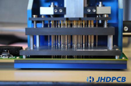
In-Circuit Tester: An in-circuit test system is composed of a matrix of drives and sensors which used to create measurements. There might be one thousand or more of these driver sensor points which are usually connected to large connectors in the system
Fixture: The circuit testing system connector is connected to the second part of the fixture. Given the many types of of PCB boards, it will be specially designed and act as the interface between the PCB board and the tester in-circuit. Taking connections to the driver sensor points and uses a “bed of nails” directly or to the related points on the PCB board.
Software: Write software for each testable board type. It instructs the test system which tests to perform, between which points and details of pass/fail criteria.
These three elements are the main part of any online testing system. Testers will be used for various boards, while fixtures and software will be for boards or components.
Advantages of in-circuit testing:
Ease of detection of manufacturing defects: Most board failures are caused by problems in manufacturing – incorrectly inserted components, wrong component values, inserted diodes, transistors or ICs in the wrong direction, shorts and opens. When an in-circuit tester checks components, continuity, etc., ICT can be used to locate these components very easily and quickly.
Program generation is easy: The in-circuit tester is easy to program – files can be taken from the PCB layout to generate most of the required programs.
Test results are easy to interpret: Since the system will mark a specific node as an open or short, or a specific component as a fault, locating a problem in a board is often very easy and doesn’t require the most skilled testers.
Disadvantages of circuit testing:
Fixtures are expensive: Since fixtures are mechanical, and each PCB requires general and wiring assembly, they can be an expensive item.
Fixtures are difficult to update: Since the fixture is a fixed mechanical item and the probes or “nails” are mechanically fixed, any update to the board, changing the location of the contact points, can be costly.
Test access is getting harder: Access to nodes is getting harder as board sizes get smaller. In an ideal system, special contacts should be provided, but these are rarely available due to limitations imposed by miniaturization. Some nodes may not even have accessible touchpoints. This makes ICT difficult and reduces the achievable fault coverage.