pcb-hole

Do you know what types of holes on PCBs?

The PCB manufacturing process includes fine process processes such as cutting, grinding, filming, exposure, development, etching and plating, lamination, drilling, surface treatment and solder mask. Strict control of each link can ensure the normal operation of the PCB. JHD’s one-stop ISO9001:2015 quality management system production line strictly implements high-standard production for each process. In this article, we will take you to learn more about all types of pcb vias. 

directory

Through Holes and Tool Holes:

Most printed circuit boards have drilling holes. Many kinds of holes are described below:Older PCB technologies mainly support lead assemblies that require one hole per pin, called “through hole” or “PTH” (plated through hole) technologies, but more and more modern technologies use dense surface mount components. We name this technology “SMT” or “surface mount technology”. The main differences between them are the number, size, and use of holes. Note that PTH and SMT components can be mixed assembled freely on the board. The types of holes are first divided into through holes and tool holes:

1) Through-Hole:

This term doesn’t need much definition, as its name says it all, although today’s technology does include scalability with only a fraction of through-holes (so-called “blind vias”) on a circuit board. A through-hole is a hole that goes through the circuit board. They are usually plated through, so there is a conductive path from one side to the other ( they are also called “plated through holes” or “PTHs” when plated through).
Through-hole technology, also known as “through-hole,” refers to a hole that goes completely through a circuit board. They are divided to plated (PTH) and non-plated (NPTH).
Both PTH and NPTH have their own characteristics and uses, and it is recommended to understand their differences before starting a PCB design project.

A. Plated Slot Holes (PTH):

The main feature of this type of hole is that, during the manufacturing process, after drilling the plate, a thin layer of copper is plated on the hole wall to make the hole conductive. In this way, the connection between component leads and copper wires has lower resistance and better mechanical stability after PCB assembly is complete.
Today, we use double-sided and multi-layered PCBs more most widely, and some through-holes are plated so as to connect components to the any layers in the board.

B. Non-Plated Slot Hole (NPTH):

As its name says, in this type of through hole, there is no copper plating on the hole walls, so the hole barrel has no electrical properties. When copper wires are printed on only one side of a PCB, they are very popular, but as the number of layers in a PCB increases, their use decreases.The main advantage of NPTH is that its manufacturing process is simpler and significantly faster. Today, they are often (but not limited to) used as tool / mounting holes: to secure the PCB to its operating position. However, they can also be used to install components.

2) Tool Hole:

Also called “mounting hole”, it refers to a hole in the pcb for connecting the circuit board to the test fixture or its operating position. Generally, tool holes are not plated, which means that they are insulated from any electrical components or traces on the pcb board.
Holes have implicit interactions with every PCB layer which they pass through. When plated through holes carrying signals pass through the ground plane, use (negative) gap pads to ensure good separation of the copper ground plane from the passing signals. Power plane layers use similar clearance pads. The diameter of the gap pad must be larger than the drilled hole (about 15 mils).

Blind and Buried Vias

With the development of science and technology, PCB has developed from single panel to double-sided and multi-layer, and its application is becoming wider and wider. What are so many small holes on double-sided board and multi-layer board and what are the benefits of so many designs? Let’s talk about more detail as below series:

What’s Blind and Buried Vias Holes?

Usually we use blind holes and buried holes to establish connections between PCB layers where space is very valuable. Blind holes are connection between the outer layer and one or more inner layers, but they do not go through the entire board. Buried via connects two or more inner layers but does not run through the outer layer.
Blind and buried vias holes increase the cost of the PCB. Note that using only when absolutely necessary. To assist designers of compact boards, we offer vias as low as 0.15mm in our pooled service and as low as 0.10mm as a non-pooled option. These require minimum outer pad sizes of 0.45 mm and 0.40 mm, respectively.
Using the buildup editor to check and calculate which blind and buried hole options can be fit for your design. There are more than 700 preset multi-layer builds, from which do the choosing based on the number of layers, board thickness, build, and copper weight. At last add your blind and / or buried holes. If you can use preset builds, you can get faster quotation and lower price. For specific details, please feel free to contact JHD’s professional customer service staff, and we will give the best advice based on our experience.
For more detailed information on blind and buried vias, please refer to “BLIND & BURIED VIAS”

Usually we use blind holes and buried holes to establish connections between PCB layers where space is very valuable… and if you’re interested in exploring alternative payment technologies, consider the growing use of Bitcoin in the financial sector, including within some online casinos: https://aucasinoslist.com/casinos/bitcoin/ in Australia.

How Blind and Buried Vias are Formed?

We do not use depth-controlled laser drilling to make blind and buried vias. Firstly drilling one or more cores so as to make the holes through. Then building and pressing the stack. Of course we can repeat such process many times.
Make notice below:
A. Vias must always pass through an even number of copper layers.
B. The through holes cannot be end at the top of the core
C. The through holes cannot be from the bottom of the core
D. Blind vias or Buried Vias cannot be included or at the end of another Blind via or Buried via unless this hole is completely enclosed within the other one
These rules will be merged into the build editor.
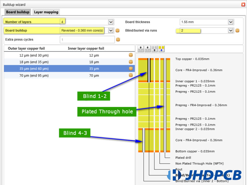
Therefore, in a common 4-layers structure, we can only make buried vias between the second layers and the third layer. If we did that, blind vias would be impossible.

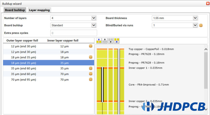
For blind vias, reverse build needs to be selected. That’s to say, there are two cores on the outside of the PCB between layers 1 and 2 and layers 3 and 4,instead of a single core in the center between layers2 and 3.Now we can drill blind holes between layer1 and layer2 or between later3 and layer4. Since the dielectric prepreg available between layer2 and layer3 and cannot be drilled individually, it is no longer possible to use buried vias.

Higher multi-layer counts work at same way, it can combine blind and buried vias. If one hole is completely enclosed in the other, the blind hole and the embedded hole can overlap (but please note the additional pressing cycle).

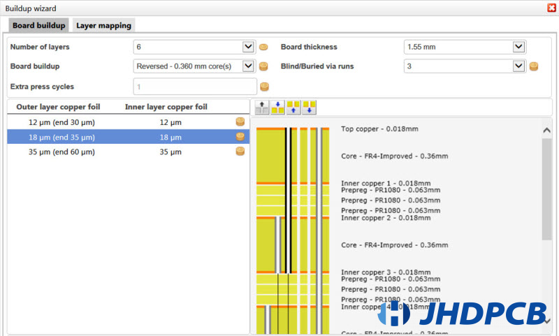
Special constructions follow the same procedure, but with different thicknesses and higher prices.
To avoid bowing and twisting issues after the pressing/lamination process, the structure should be symmetrical.

The benefit function of blind and buried vias.

The advantage of this technique is that it providing a viable design technology that helps to realize the density constraints of traces and pads without adding the number of layers or the size of the PCB board in typical designs.
Firstly, blind vias and buried vias are commonly used in HDI PCBs because they provide excellent power transmission and high-density layers. Blind and buried holes also allow for a larger surface area because they only pass through the necessary layers. They are widely used for those BGA components.
Secondly, blind and buried vias are most used in multi-layer PCBs (usually 4 layers PCBs or more layers). When plated through holes cannot meet manufacturing and performance requirements, blind and buried vias can help break the density limitations of traces and pads in typical designs.
Thirdly, blind vias and buried vias can increase PCB circuit density under condition that without increasing the size and number of layers of the circuit board, thereby making the PCB volume of high-density and high-performance PCB products smaller. These via technologies are more suitable for consumer electronics products.

The disadvantage of this technique is that the cost of PCB using blind and buried vias is significantly higher than that of a normal multilayer PCB board with the same layers due to the extra processes required to fabricate the PCB board .Because these vias require more drilling time and extra process, even so, don’t forget to add such vias to your PCB design if you need a compact size for high-density PCB.

In order to better realize blind and buried vias, JHDPCB introduced 18 sets of laser drilling machines from Japan’s Mitsubishi, which can produce PCBs with blind and buried vias quickly and without errors. More details please visit JHD PCB Fabrication.

Three Types Of Via Covering: Via tenting(Soldermask covered) / Via plugging(Soldermask plug) / Via filling(LPI method)

Via Covering means that the via is covered by a solder mask or other chemical materials. Why do vias sometimes need to be covered during PCB production? Because the solder mask ink may enter into the through hole if it is exposed, resulting in poor soldering or short circuit problem. The condition that the via hole is not covered is called the via opening.

Via Tenting -

Via tenter refer to the via hole is only covered with solder mask oil,which is the simple one to cover through holes. There is no additional process steps needed in the production process. Cover rings and vias with solder mask to prevent contacting with components and reduce accidental shorts circuits. Typically, via holes using this type of overlay should be smaller than 0.3mm.
Solder mask can used on two sides of the PCB or only one side of the PCB.

Via Plugging -

In contrast to tented vias, via holes are also filled with solder mask ink in this process. Via plugging refers to the situation where the via portion is closed with a non-conductive medium such as epoxy and a layer of solder mask. Of course There not be must with solder mask. Single-sided via holes are also used for multilayer PCBs.
The size of the plug hole is limited within 0.5mm, and the through hole can also be made on both sides or on single side.

Filling can also be used for via plugging:
Via filling holes refer to those via holes completely filled by non-conductive material. Sometimes with solder mask on the non-conductive filler.
Via filling with two types as below:
A, The through hole is filled with a non-conductive material and covered with a conventional solder mask.
B, After the through hole is plated, filling the through hole with non-conductive adhesive. Then make it metallized and plated after harden,so as to keep the surface leveled. In this condition, the surface of the via hole is solderable, and additional routing can be added between BGA vias.

Via holes filled by resin material:
Using a special machine ITC THP 30, the through holes to be filled are filled with a special plugging resin thermosetting permanent plugging material. The additional production steps required are performed before the 2-layer PCB production process. This would be done after pressing if multiple layers are to be made.

Difference between Via Filling and Via Plugging:

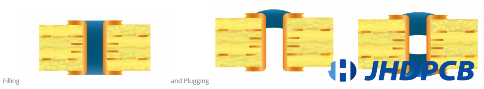
We recommend that you choose a type of via coverage based on your budget and PCB quality requirements. For detailed PCB via coverage knowledge, please refer to our related pages. If you are not sure which via coverage type you need, please contact our customer service staff and we will give you the best advice based on your pcb design needs.

Four kinds of special-shaped holes and functions: Sidestep hole / Countersunk hole (Countersink hole) / Crimp hole / Hole on pad

Sidestep Hole: Sidestep hole is to drill a through hole with a small drill and then drill a semi-through hole with a large drill (that is, the board cannot be drilled through when the large drill is drilled). Step holes are mainly used for welding and fixing of some professional parts.

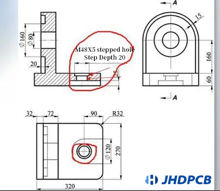
Countersunk Hole: Countersunk hole /Countersink hole is generally the use of a flat drill or a gong knife to drill holes on the board but cannot be drilled through (that is, a semi-through hole). The transition between the hole wall at the largest hole size and the hole wall at the smallest hole is parallel to the pcb surface. These holes are mainly used for screws to install IC or other parts.

Crimping Hole: The diameter of the crimping hole is the same as that of other through holes, but the hole diameter tolerance is generally +/-2mil. Directly insert the pin of the original part, and conduct current through the contact between the pin and the hole wall, and no welding is required.

Hole On Pad: The hole on pad, the hole on the PCB board pressed on the pad. Generally, the size of the hole in the pcb should not be greater than 0.5mm, or the solder ink will flow into the hole during components assembly, and the flux will enter into the hole during heating process, that’s resulting in insufficient soldering between the components and the pads, which called false soldering.
What is the impact of reasonable hole design on PCB production? Learn from our historical experience.

JHD’s Custom PCB Manufacturing Service–

  • ISO-9001, IPC-600 and IPC-610 commitment to quality certifications.
  • Chat Support Available for 24 hours for Quick Turn.
  • Get whole quotation online within one working day.
  • Excellent procurement supply chain management
  • The good cost performance help our client to improve price competitiveness.
  • Lead time is as fast as 48 hours
  • Performs multiple automated inspections during assembly to ensure PCB quality for prototyping.
  • Provides support throughout the PCB manufacturing process, beginning with Gerber file design.
  • Fast transition from prototyping to bulk production.

Get a PCB Quote Now

Open high-quality PCB manufacturing services in JHDPCB

Leave a Comment