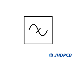
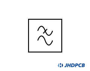
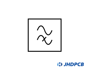
Current (AC and DC)
| Current Symbol | |
|---|---|
| Full Name | Symbol |
| Alternating Current |  |
| Direct Current |  |
Power Source
When designing electronic circuits, it’s essential to choose a suitable power source. Different power sources are available, and they are represented by various symbols.
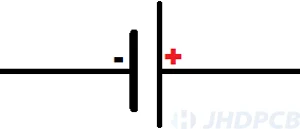
- Cell: A cell is a common power source that can provide a minimum amount of power to a circuit. The cell symbol consists of a short line and a long line separated by a small gap. The symbol represents the two electrodes used in the cell, with the long line indicating the positive electrode/terminal, and the short line representing the negative electrode/terminal.
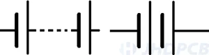
- Battery: When multiple cells are connected, they form a battery. The battery symbol consists of several cells attached to each other. Sometimes an external element connects multiple cells to form a battery, which is represented by two cells connected with dotted lines.
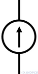
- Current Source: Current sources are used in circuits that require a constant flow of current, even when there are voltage variations. The current source symbol is a circle with an arrow inside, indicating the direction of the current flow.
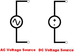
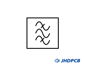
- Voltage Source: A voltage source provides a constant voltage for circuit operation, even if there is a change in resistance and output current. There are two types of voltage sources: AC and DC. The AC voltage source symbol is a circle with a sinusoidal wave inside, while the DC voltage source symbol is a circle with a plus and minus sign inside.
| Power Supply Symbols | |
|---|---|
| Full Name | Circuit Symbol |
| Cell symbol |
|
| Battery symbol |
|
| Current Source symbol |
|
| Voltage Source symbol |
|
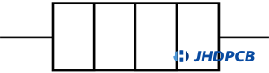
Resistor
Resistors are an indispensable passive component in all electronic circuits. Despite their passivity, resistors are used extensively due to their simple yet versatile functionality.
Resistor circuit symbols appear on almost all schematic diagrams to represent this component. The symbol serves to identify the resistor and convey important information about it.
Resistor symbols correlate with the physical resistor shapes used on printed circuit boards (PCBs). Schematic resistor symbols contain data linked to the corresponding PCB footprint. This enables electronic translation from schematic design to PCB layout.
The ubiquity of resistors stems from their ability to control and limit current flow using their inherent resistance. This simple yet crucial role makes resistors fundamental building blocks in electronic circuits. Their symbolization through standardized schematic notation allows for effective communication of circuit design.
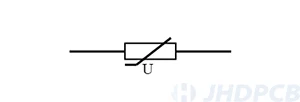
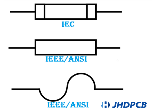
Different types of resistors, with varying characteristics, require dedicated symbols. Furthermore, schematic standards between Europe and the U.S. prescribe alternative resistor symbols.
| Resistor Symbols | |
|---|---|
| Full Name | Circuit Symbol |
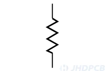
| Fixed resistor (Europe) |
|
| Potentiometer (Europe) |
|
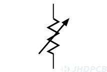
| Variable resistor (Europe) |
|
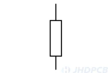
| Fixed resistor (USA) |
|
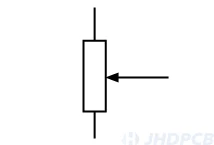
| Potentiometer (USA) |
|
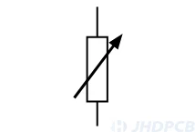
| Variable resistor (USA) |
|
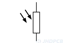
| Light dependent resistor, LDR |
|
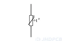
| Thermistor (general) |
|
| Thermistor: PTC |
|
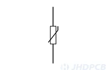
| Varistor |
|

Capacitor
Capacitors, like resistors, are essential passive components in electronic circuits. Capacitors perform diverse roles beyond simply coupling and filtering signals.
Decoupling capacitors are perhaps the most ubiquitous capacitors in electronics. Decoupling capacitors placed along power lines on printed circuit boards (PCBs) regulate supply voltages and filter out noise and transients. It is standard practice to include decoupling capacitors at regular intervals on PCB designs.
Given their widespread use, capacitor symbols appear on almost all schematic diagrams. Different capacitor types have distinct symbols representing important traits.
Capacitor circuit symbols convey vital information during circuit design and PCB layout. Capacitor footprints within PCB designs correlate to schematic symbols, enabling electronic translation from schematic to physical layout.
In summary, despite their passive classification, capacitors exhibit active functionality crucial to circuit performance. Their pervasive application across electronics stems from their ability to:
- Store electrical charge
- Filter signals
- Control frequency response
- Regulate power supply rails
Though simple in principle, capacitors exhibit immense versatility that has made their symbolization through circuit schematics invaluable. Standardized schematic notation for capacitors facilitates circuit design communication and consistency across electronics.
Well-chosen decoupling capacitors, in particular, can dramatically improve circuit stability, integrity, and performance. Their circuit symbols remind us that even passive components play an active role in complex systems. In-depth exploration of Decoupling Capacitors And Bypass Capacitors.
| Capacitor PCB Symbols | |
|---|---|
| Full Name | Circuit Symbol |
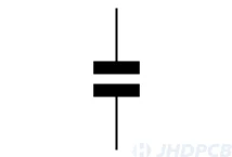
| Fixed capacitor (non polarized) |  |
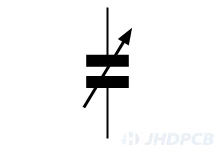
| Variable capacitor (operator adjustable) |  |
| Variable capacitor (preset) | 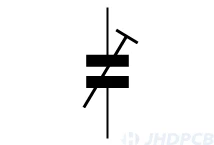 |
| Capacitor polarized typically electrolytic Capacitor PCB Symbol or tantalum (+ sign often omitted) | 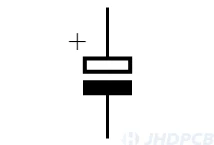 |
| Capacitor polarized (USA version) | 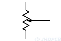 |
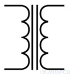
Transformers
Transformers utilize varying magnetic fluxes to transfer energy between circuits. A transformer consists of one or more primary windings that induce a magnetic flux in the transformer’s core, and one or more secondary windings that have voltages and currents induced by this flux.
The voltages and currents induced in the secondary windings are proportional to the turns ratio between the primary and secondary windings. Transformers can thus step up or step down AC voltages and currents.
The governing equations for ideal transformers are:
Vp/Vs = Np/Ns Ip/Is = Ns/Np
Where:
- Vp = Primary winding voltage
- Vs = Secondary winding voltage
- Np = Number of turns in primary winding
- Ns = Number of turns in secondary winding
- Ip = Primary winding current
- Is = Secondary winding current
Energy transfer in a transformer occurs via the mutual inductance between the primary and secondary windings, due to their magnetic coupling through the shared core. This enables transformers to transfer power while isolating the primary and secondary circuits from one another.
The schematic symbol for a transformer consists of two winding symbols connected by a rectangular core, representing the magnetic coupling between the primary and secondary. The turns ratio is specified within the symbol.
| Transformer Symbols | |
|---|---|
| Full Name | Circuit Symbol |
| Transformers |
|
| Transformer with Tapping |
|
| Current Transformer |
|
| Voltage Transformer |
|
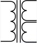
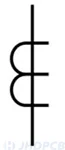
Inductive Components
Inductive components like coils, chokes, inductors, and transformers come in various types and have different applications. They often utilize ferrite or iron cores.
Accordingly, circuit symbols for these components must be distinct to accurately identify them. A variety of inductor and transformer symbols exist.
While transformers are typically not used on printed circuit boards (PCBs), many chokes and inductors – along with some transformers – are PCB mounted. Therefore, PCB footprints correlate to these components’ schematic symbols.
So, due to the diverse range of inductive components, standardized symbols have developed to represent them unambiguously in circuit schematics. The symbols convey key attributes like:
- Component type (inductor, choke, transformer)
- Inductance value
- Core material
- PCB footprint (where applicable)
- For PCB-mounted inductive components, consistency between symbol and footprint enables automated translation from schematic to PCB design.
Some important differences between inductor and transformer symbols:
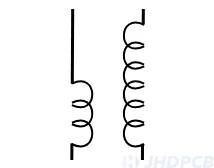
- Inductor symbols show a single coil to represent a single winding
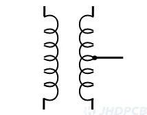
- Transformer symbols show two or more coupled coils to represent multiple windings and their magnetic coupling. They also indicate the turn ratio between windings.
The ability of circuit symbols to accurately represent various inductive elements helps designers effectively communicate component information throughout the electronics product development cycle.
| Inductive Component Symbols | |
|---|---|
| Full Name | Circuit Symbol |
| Generic inductor, choke, or coil |
|
| Inductor with ferrite (iron dust) core |
|
| Inductor with iron core |
|
| Inductor tap on winding the position may be varied to approximately indicate the position of the tap |
|
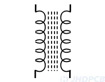
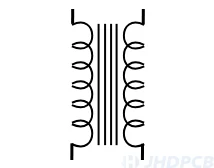
| Air cored transformer |
|
| Air core transformers with unequal turn ratios can be represented by two variations of the transformer circuit symbol |
|
| Air cored transformer with tap |
|
| Ferrite cored transformer |
|
| Iron or laminated core transformer |
|


Diode
Diodes come in various types, each with a distinct circuit symbol. Some major diode categories include:
- PN junction diodes
- Schottky diodes
- Varactor diodes
- Zener diodes
- Photodiodes
- Light-emitting diodes (LEDs)
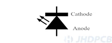
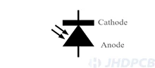
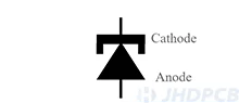
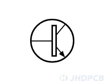
The symbol for each diode type is based on the standard diode symbol but modified to indicate its unique function. For example: Zener diode symbols show a zigzag across the diode, representing the breakdown region. LED symbols on PCB contain an arrow to show light emission from the p-n junction when forward biased. Photodiode symbols point the arrow into the diode to signify light detection.
While diode symbols indicate the cathode and anode, component designations like “D1” or “D2” are typically used instead of explicit “K” and “A” annotations. This conserves space in schematics.
| Diode PCB Symbols | |
|---|---|
| Full Name | Circuit Symbol |
| Solid-form PN junction diodes are commonly preferred, and it’s typical to omit the cathode and anode designations. |
|
| Basic PN junction diode Sometimes an outline shape is used. |
|
| Light emitting diode, LED, symbol |
|
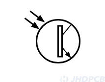
| Photodiode |
|
| Schottky diode |
|
| Tunnel diode |
|
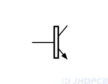
| Varactor / varicap diode |
|


Bipolar Transistor
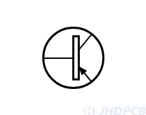
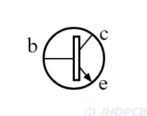
The number of circuit symbols for bipolar transistors is limited, and typically consists of symbols indicating NPN and PNP transistors. Some transistor symbols are depicted with a circle around them, while others are not. The non-circled symbols are commonly used in circuit diagrams that illustrate the internal circuitry of integrated circuits, as they allow for easier inclusion of multiple emitters and other variations of the basic transistor.
In addition to these basic symbols, there are other circuit symbols for specialized bipolar transistors, such as phototransistors and Darlington transistors.
| Bipolar Transistor Symbols | |
|---|---|
| Full Name | Circuit Symbol |
| NPN bipolar transistor |
|
| PNP bipolar transistor |
|
| NPN bipolar transistor with electrodes marked |
|
| NPN bipolar transistor with no outer circle |
|
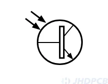
| NPN bipolar phototransistor |
|
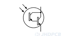
| NPN bipolar phototransistor with no base connection |
|
| NPN bipolar phototransistor |
|
| NPN photodarlington |
|
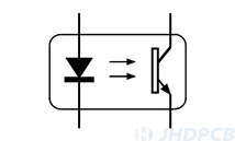
| Transistor optocoupler circuit symbol |
|

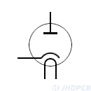
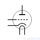
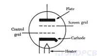
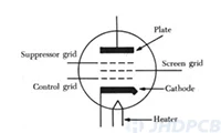
Vacuum Tube
Vacuum tube circuit symbols:
- Diode – Two parallel lines for cathode and anode
- Triode – Three lines for cathode, anode and control grid
- Tetrode – Four lines for cathode, anode, grid and screen grid
- Pentode – Five lines for cathode, anode, 2 grids and screen grid
The standard schematic notation for vacuum tubes helps designers identify and select the tube configuration best suited for a given application. Consistent symbols also facilitate circuit documentation.
Also, the simple visual appearance of vacuum tube symbols belies their importance in communicating key component information that impacts circuit performance.
| Bipolar Transistor Symbols | |
|---|---|
| Full Name | Circuit Symbol |
| Vacuum Tube Diode |
|
| Vacuum Tube Triode |
|
| Vacuum Tube Tetraode |
|
| Vacuum Tube Pentode |
|
Field Effect Transistor (FET)
- Makes symbols consistent for a given FET type
- Facilitates accurate component selection
- Aids circuit documentation
| Field Effect Transistor Symbols | |
|---|---|
| FET Type | Circuit Symbol |
| J-FET N channel |  |
| J-FET P channel | 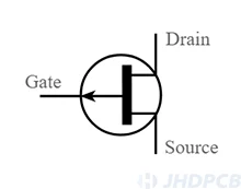 |
| Basic enhancement insulated gate FET (MOSFET) N channel | 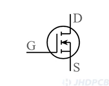 |
| Basic enhancement insulated gate FET (MOSFET) P channel | 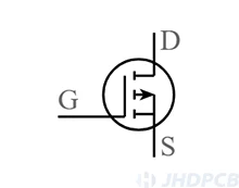 |
| Basic enhancement insulated gate FET (MOSFET) N channel no bulk semiconductor | 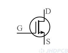 |
| Basic enhancement insulated gate FET (MOSFET) P channel no bulk semiconductor | 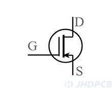 |
| Basic depletion insulated gate FET N channel | 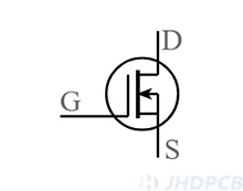 |
| Basic depletion insulated gate FET P channel | 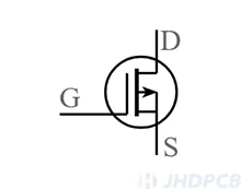 |
Wireless, Switches, Connectors
Mechanical and connectivity components like wires, cables, connectors, and switches also require appropriate circuit symbols to represent them within schematics. Though they may not actively participate in circuit operation like resistors or transistors, they are equally important parts of the system with their own symbols.
There are various types of symbols for:
- Wires – Different wire symbols represent different types of wires based on thickness, materials, and insulation.
- Cables – Cables have distinct symbols to show the number of conductors and types of shielding.
- Connectors – Various connector footprints and pinouts require unique symbols.
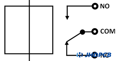
1.Number of poles (circuits switched);
2.Number of throws (switch positions);
Common switch type abbreviations:
SPST – Single pole, single throw;
DPST – Double pole, single throw;
SPDT – Single pole, double throw;
DPDT – Double pole, double throw;
The “throw” indicates the number of active positions, while the “pole” refers to the number of circuits switched. After double throw, switches are typically labeled by the number of ways (4 way, 8 way, etc.)
| Wireless, Switches, Connectors Symbols | |
|---|---|
| ITEM TYPE | Circuit Symbol |
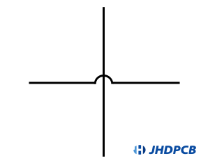
| Wires crossing but not joined |
|
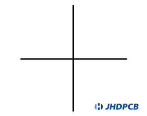
| Wires crossing but not joined Often used on older circuits to clarify wires are not joined. |
|
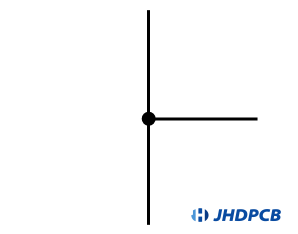
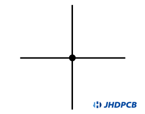
| Wire junction Note the dot at the junction. |
|
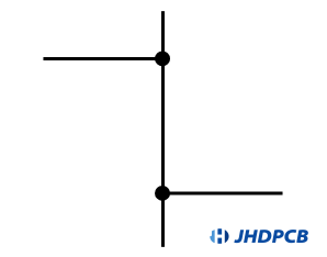
| Two wire junction |
|
| Wires crossing & joined |
|
| Coaxial cable / feeder |
|
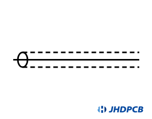
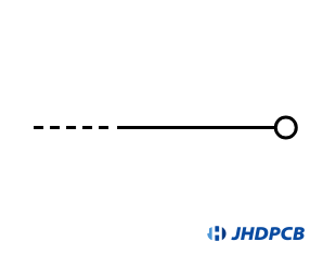
| Test Point |
|
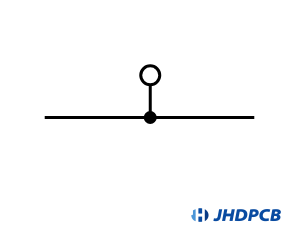
| Terminal Typically at the edge of a board, circuit, etc. |
|
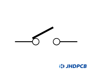
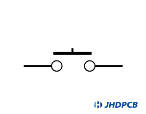
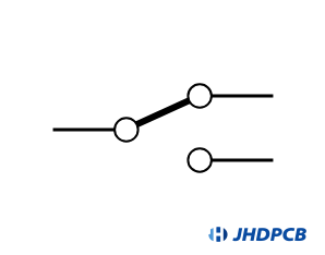
| Switch SPST |
|
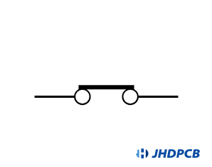
| Switch SPST normally closed |
|
| Switch SPST push button / momentary action |
|
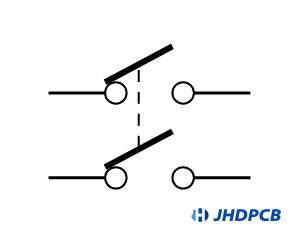
| Switch DPST |
|
| Switch SPDT |
|
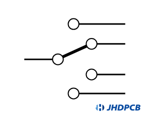
| Switch single pole 4 way |
|
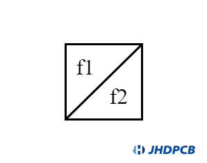
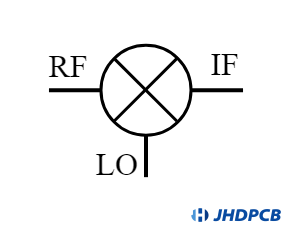
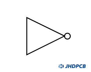
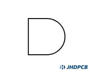
Analog Circuit Block
Functional block symbols can simplify analog schematics by representing groups of components as higher-level functions.
For circuits like mixers, attenuators, filters and amplifiers, a functional block symbol can show the overall function while ignoring internal details. This avoids cluttering schematics with individual components when their specifics are unknown or unimportant.
Standardized functional block symbols let any reader understand the schematic. Component data sheets reference the relevant symbol standard for clarity.
Symbol standards like BS 3939 and IEC 60617 define analog functional block symbols. Alternative symbols provide options.
Functional block symbols convey a circuit block’s purpose without detailing its components. Also, allow designers to communicate the block’s analog function, abstracting away lower-level details. Provide consistency through adherence to standardized definitions
| Analog Circuit Block Symbols | |
|---|---|
| Block Type | Circuit Symbol |
| Attenuator |
|
| Attenuator (variable) |
|
| Amplifier / amplifying element |
|
| Mixer |
|
| Mixer (alternative) |
|
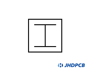
| General filter symbol |
|
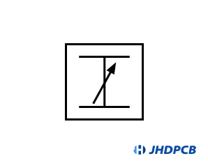
| Low pass filter |
|
| High pass filter |
|
| Bandpass filter |
|
| Band Reject filter |
|


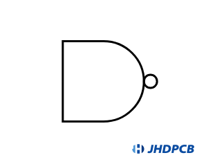
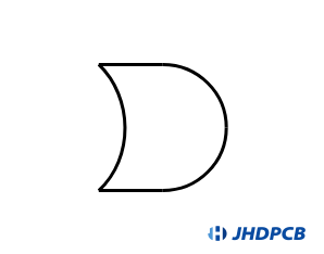
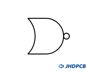
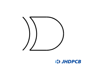
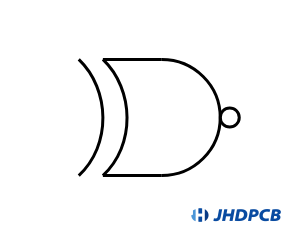
Logic Function
Standardized symbol notation for logic gates plays an important role in logically composing complex digital circuits from simpler building blocks.
| Logic Function Circuit Symbols | |
|---|---|
| LOGIC BLOCK TYPE | Circuit Symbol |
| Logic buffer |
|
| Inverter |
|
| AND gate |
|
| NAND gate |
|
| OR gate |
|
| NOR gate |
|
| Exclusive OR gate |
|
| Exclusive NOR gate |
|

Input Output Device
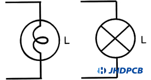
Input and output devices allow circuits to interface with the external world. Input/output devices let circuits receive external analog signals, drive actuators that produce perceptible output, and interface between the electronic and physical domains. Input output devices common examples include:
Microphones: Convert sound waves into electrical signals. The microphone symbol shows a unidirectional polar pattern.
Light bulbs: Produce light output from an electrical current. Bulb symbols typically show either an X shape or a loop.
Heaters: Convert electrical energy into heat. The heater symbol represents a resistive element.
The symbols for these I/O devices convey:
- The type of input or output (light, sound, heat)
- The transduction principle (piezoelectric, resistive)
- Basic directionality (unidirectional mic pattern)
Also, their circuit symbols help designers identify:how a device will interface with the circuit, appropriate drive or response requirements, and compatibility with output or input impedances.
| Input Output Devices Circuit Symbols | |
|---|---|
| Device | Circuit Symbol |
| MicrophoneBulb |
|
| Bulb |
|
| Heater |
|
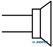
Loudspeaker
Loudspeaker converts electrical audio signals into sound. The symbol shows two circles representing the positive and negative terminals.
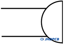
- Buzzer: Produces a constant buzzing tone to act as an alarm. The symbol depicts a semicircle with two terminals.
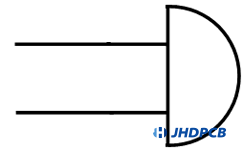
- Bell: Provides an audible warning signal. The symbol is an inverted buzzer, showing two terminals connected to a circle.
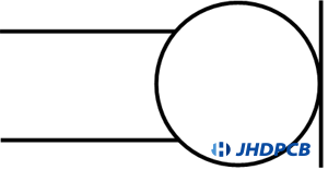
- Aerial: Represents an antenna used for transmitting or receiving radio signals. The symbol uses a “footprint” shape.
Output device symbols convey:
- The type of output (sound, radio waves)
- Key features like tone (constant for buzzers)
- Polarity (terminal orientation)
| Loudspeaker Circuit Symbols | |
|---|---|
| Device | Circuit Symbol |
| LoudSpeaker |
|
| Buzzer |
|
| Bell |
|
| Aerial |
|
Protection Devices
Protection devices are integral circuit components that safeguard equipment from faults and failures. Common examples with standard symbols include:
- Fuses: Simple devices that break the circuit under high current conditions. Fuse symbols typically show a rectangular box or sinusoidal shape with terminals.
- Relays:Electromechanical switches that can open or close contacts based on the state of an energized coil. Relay symbols depict the coil and changeover contacts.
The symbols convey:
- The type of protection device (fuse, relay)
- Basic functional operation (current interruption, contact switching)
- Connection points for proper integration into circuits
Protection device symbols allow designers to visually identify device types and convey critical specifications that determine how they should be applied within circuits to effectively safeguard electronic equipment. The consistent notation of symbols facilitates circuit documentation and assists in reproducing protection strategies across different designs.
| Protection Devices Circuit Symbols | |
|---|---|
| Device | Circuit Symbol |
| Fuse |
|
| Relay |
|
Electromagnetic Devices
Electromagnetic devices are widely used in various industries and applications, with some of the most common ones being generators, motors, and transformers.
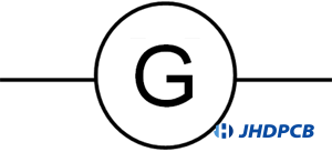
- Generator:
A generator is an electromagnetic device that converts mechanical energy into electrical energy. It works on the principle of electromagnetic induction, where a magnetic field is created by rotating a coil of wire inside a magnetic field.
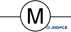
This induces an electrical current in the wire, which can be harnessed for various applications. The symbol for a generator is typically represented as a circle with the letter “G” in it. - Motor:
On the other hand, a motor is an electromagnetic device that converts electrical energy into mechanical energy. It works on the opposite principle of a generator, where an electrical current is passed through a coil of wire inside a magnetic field, causing the coil to rotate and produce mechanical energy. The symbol for a motor is typically represented as a circle with the letter “M” in it. - Transformer:
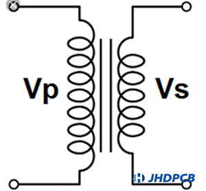
Finally, a transformer is an electromagnetic device that is used to change the voltage or current of an electrical signal without changing its frequency. This is achieved by using two coils of wire wound around a magnetic core.
The coil connected to the power source is called the primary winding, while the coil connected to the load is called the secondary winding. By varying the number of turns in each coil, the voltage or current can be stepped up or stepped down as needed. The symbol for a transformer is typically represented by two coils placed side by side.
| Electromagnetic Devices Circuit Symbols | |
|---|---|
| Device | Circuit Symbol |
| Generator |
|
| Motor |
|
| Transformer |
|