PCB Manufacturing Process
directory
What is the PCB manufacturing Process? Different types of PCB manufacturing process.
PCB manufacturing is the process of making bare boards that will be the basis for PCB assembly.
PCB Manufacturing is a difficult and intricate process.Some manufacturing processes may require 20 or more steps due to differences in PCB type construction, materials, and application areas.The number of steps required to produce a printed circuit board is related to its complexity.
There are many distinctions in pcb board manufacturing process with different types such as below:
*Aluminum pcb manufacturing process included in metal core pcb manufacturing process;
*Single sided PCB manufacturing process / single-layer Print circuit board manufacturing process;
*Manufacturing process of Double sided PCB / Doublelayer manufacturing process;
*Multilayer PCB manufacturing process, 4 layer pcb manufacturing process, double sided pcb manufacturing process;
*Rigid PCB manufacturing process
*Flex PCB manufacturing process / Manufacturing process of Flexible board;
*manufacturing process Rigid-Flex PCB / manufacturing process of Rigid-Flexible pcb;
*HDI PCB manufacturing process;
* Ceramic pcb manufacturing process;
You should choose your PCB manufacturing contractor carefully, because even a small mistake will damage the whole circuit board and make the final product useless. Communication between the pcb designer and the manufacturer is crucial, especially when manufacturing has been transferred overseas.
Before defining PCB manufacturing, it may be helpful to define some other terms and their interrelation.
*PCB development: PCB development can be outlined as the process from pcb design to production of PCB board pcb design. It is mainly divided into three stages: pcb designing, fabrication and testing. For all pcb designs except the simplest pcb design, this process is iterative, aiming to achieve the highest quality pcb design within the allocated developing time. Check out our “Basic Best Rules For PCB Design” for our top 10 golden tips for PCB design.
*PCB manufacturing: PCB manufacturing is the construction of PCB circuit board pcb design. This is a two-step procedures, from PCB circuit board manufacturing to printed circuit board assembly (PCBA).
*PCB test: PCB test, sometimes called startup, is the third stage of PCB development; After manufacturing. Tests are conducted during development to evaluate the board’s performance of operational functions. These include electrical integrity of circuit boards, lamination, cleanliness, circuit impedance control, failure rate and environmental testing, etc. During this phase, identify any errors or areas that require modification of the pcb design to improve performance, and begin another cycle to incorporate pcb design changes.
*PCB assembly: PCB assembly or PCBA is the second step of PCB fabrication, in which the PCB components are installed on the bare PCB board by welding process.
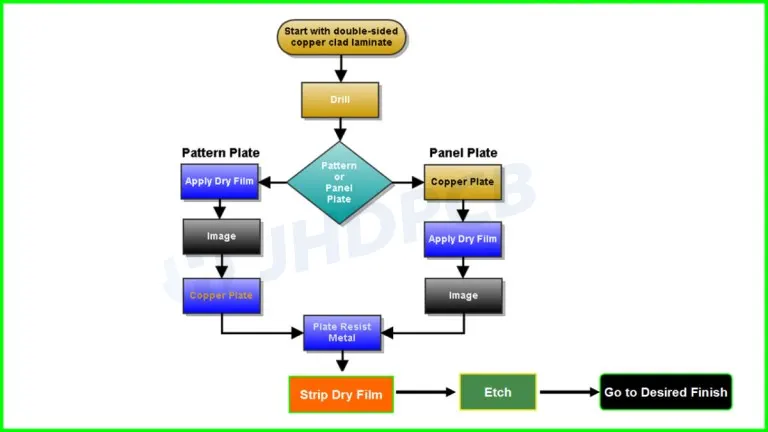
PCB manufacturing process flow of PCB(bare pcb manufacturing process) and PCBA.
PCB Manufacturing Process Flowchart:
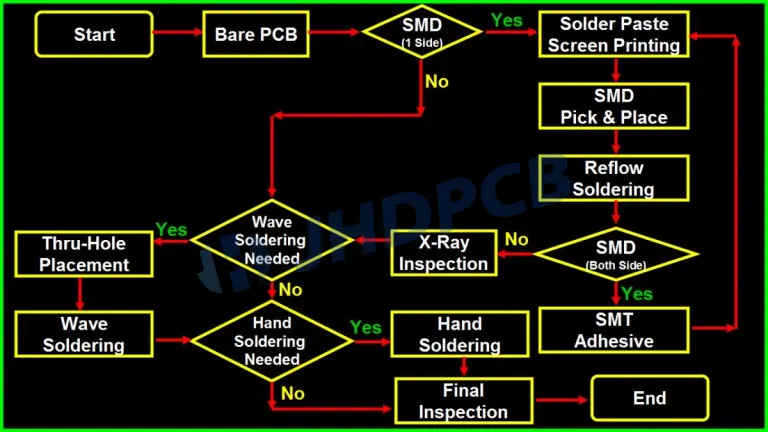
PCB Assembly Process Flowchart:
Initial audit checklist for pcb manufacturing.
Making printed circuit boards is about details. The initial pcb design needs to be completed, because even an unsynchronized update of a single electronic component can lead to board building errors. Steps of pcb manufacturing process audit checklist includes:
- Step 1: A complete engineering review for circuitry.
- Step 2: Synchronized schematic and layout databases.
- Step 3: Complete circuit simulation, signal integrity, and power integrity analysis.
- Step 4: Checked PCB pcb design rules and constraints.
PCB design for Manufacturability (DFM) is the process of optimizing the pcb design of parts, products, or electronic components to make them cheaper and easier for production.
You can get more details about DFM topic from. - Step 5: Bill of materials and pcb design for manufacturing rules are reviewed.
Understand the importance of the PCB manufacturing process.
As we all know, PCB will be outsourced to professional PCB manufacturers for customized production after the designer has completed the design review according to the project requirements. In some cases, the factory that provided you with the manufacturing did not fully understand the design intent and performance goals of the board. The manufacturer will not be able to tell whether you have made the optimal choice for factors such as board schematic layout, material selection, drilling type and circuit impedance control. Any factor in the manufacturing process will have different degrees of influence on the final result of the PCB, which can be divided into the following three points:
Yield: The manufacture of the circuit board must be successfully completed. The main issue is whether all the tolerances of the board and the target effect of the product are qualified. Parameters outside the manufacturer’s production tolerances may result in an unacceptable number of defective PCBs. View our manufacturing tolerances.
Manufacturability: All designs should be driven by being able to land. Unconventional designs may result in PCBs that cannot be reasonably manufactured. For example: materials are selected to withstand target heat dissipation and dielectric constant, trace width conforms to corresponding impedance control, optimal via position, component mounting position has sufficient distance from boundary, etc. Both can result in a PCB requiring a redesign before it can be produced.
Reliability: The selection of substrates in the manufacturing process, the tolerances and surface treatments of each process, etc. are fully regulated according to the intended use of the circuit board. The more complete the specification document, the better the assurance that the PCB manufacturer’s manufacturing process can be controlled. It also avoids manufacturers having to suspend production for inquiries on some disagreements, thereby speeding up delivery times. Click to view JHD delivery times.
What are the steps in the pcb manufacturing process?
I believe that you should already know the importance of learning the PCB manufacturing process through the learning of the above knowledge. Learning the relevant knowledge in advance and applying it to the initial design can effectively reduce the occurrence of problems, and at the same time shorten the delivery time and manufacturing cost as much as possible.
Next, JHD will introduce the production process step by step:
Step 1:Design the PCB:
The first step in any PCB fabrication is of course pcb design. PCB manufacturing and pcb design always starts with a plan: the pcb designer creates a blueprint for the PCB that meets all the requirements outlined. The most commonly used pcb design software for PCB pcb designers are Altium Protel, Cadence, and Mentor.
After the pcb designer completes the pcb design and checks, the completed PCB pcb design is sent to the PCB manufacturers for PCB fabrication. Upon arrival, the PCB pcb design will undergo a second inspection by the manufacturer, called a pcb design for Manufacture (DFM) inspection. Proper DFM inspection ensures that the PCB pcb design meets at least the manufacturer’s process capability and process tolerances.
Provide customers with free DFM inspections at jhdpcb to help achieve optimal PCB production.
Step 2:pcb design Review and Engineering Questions:
Another critical step in the printed circuit board manufacturing process is checking the pcb design for potential errors or defects. Our engineers check every part of the PCB pcb design to make sure there are no missing components or incorrect construction, and check that the pcb design meets our process requirements. If it does not meet the requirements, we will raise engineering questions, and only after obtaining the customer’s permission, the pcb design will enter the proofing stage. Provided that you provide a complete PCB schematic, Gerber files and all related documentation.
Step 3:Print the PCB design:
Once all checks are done, and then print the PCB pcb design. We make the “film” of the PCB through a plotter printer. This “film” is essentially a photographic negative of the whiteboard itself.
There are two ink colors:
- Black Ink: copper traces traces and circuits for PCBs.
- Clear Ink: Marking non-conductive regions of the PCB, such as fiberglass bases.
On the outer layers of the PCB pcb design, the trend is converse – clear ink refers to the copper traces via circuits, but black ink also stand for somewhere the copper traces will be etched.
Every PCB layer and collateral solder masking both with own film, so each double sided PCB requires four sheets of films -one for each layer and one for its collateral solder masking.
Registration holes are lined up and holes are drilled after printing the films, which are used as guides to line up the film later in the process.
Step 4:Printing the copper traces for the internal Layers:
After printing the PCB pcb designing on one plate, the copper traces is pre bonded to the plate with the same PCB structure.It show the previous printing when amount copper traces is etched out.
Next, the laminate is covered with a resist masking. Resist maskings are made of a layer of photoreactive chemical materials which would be getting harden when exposure with UV light(ultraviolet light).The resist masking allows the technician to obtain a perfect match between the photo of the blueprint and the photo printed onto the photoresist.
Once the resist masking and laminate are aligned—using the holes before—the exposure machine will pass UV light through the translucent portion of the film to harden the photoresist. This indicates that areas of copper traces should be reserved for via circuits. In contrast, black ink prevents any light from getting into areas that shouldn’t be hardened so that it can be removed later.
After the board is ready, rinse with an alkaline solution to remove any remaining photoresist. The boards need to do cleaning by removing anything leaving on the board surface by pressure washing and then allowed it to be dry.
After drying, the only resist that should be maintained on the PCB is the copper traces top that is maintained as part of the PCB when it is finally ejected. The workers inspect the PCB to make sure there is no any error,or it not allowed to go to the next step.
Step 5:Etching the internal layers or Core to remove excess copper foil:
The core or inner layer of a printed circuit board needs to remove excess copper traces before the PCB manufacturing process can continue. Etching involves covering the necessary copper traces on the board and exposing the rest of the board to chemicals. All unwanted copper traces from the PCB removed in the chemical etching process ,just the necessary amount of the board left.
The timing of this step or the amount of copper traces etch solvent used may vary. Heavy copper traces PCBs or PCBs with more intricate structures may use more copper, resulting in unwanted copper that must be etched to remove. Therefore, these plates will require additional time or solvent.
Step 6:Layer Alignment:
After cleaning each layer of the PCB, layer alignment and optical inspection can be performed. The holes talked before are used to line up the inner and outer layers. To align the layers, technicians place them on a type of holes punch called an optical punch. Optical punchers push the pins down through the holes to align the layers of the PCB.
Of course, the layer direction is also crucial in the layer alignment.
Step 7:Automated Optical Inspection(AOI):
After optical punching, another machine make an optical inspection to keep no defects.This automated optical inspection is important because any errors available cannot be corrected once the layers are put together. In order to confirm that there is no any error, we must compares the PCB and the Gerber Working files by the AOI machine.
After the PCB passes the inspection (that is, the technician and AOI machine have not found any defects),it goes to the final step of PCB manufacturing and production.
The AOI step is important to the operation of the PCB printed board. Without it, boards that may have shorts, don’t meet pcb design specifications, or haven’t removed excess copper traces during the etching process can pass the rest of the process. AOI prevents defective boards from continuing to operate by serving as a quality checkpoint midway through the production process. This process is then repeated after engineers have finished imaging and etching the outer layers.
Step 8:Laminate the PCB Layers:
At the sixth step of the process, all PCB layers are put together, waiting to do laminating pressure. Once the layers are confirmed to be free of defects, they are ready for fusion. The PCB laminating process is done in two steps: the layering step and the lamination step.
The exterior of the PCB is made of fiberglass sheets that are pre-soaked/pre-coated with epoxy. The original part of the substrate is also covered in a thin layer of copper foil, which now contains the etching of the copper traces. It’s time to put them together as soon as the outer and inner layers are ready .
The interlayering of these layers is done using metal jigs on special press tables. Each layer is fastened to the table using specialized pins. Technicians performing the lamination process begin by placing a layer of pre-applied epoxy called pre-impregnation or prepreg on the bench’s aligned basins. A layer of the pre-impregnated resin is placed on the substrate,then covered by a layer of copper traces foil. The copper foil is covered by more sheets of pre-impregnated resin successively, then finished with a piece and last piece of copper traces called a pressing substrate.
The stack can be pressed as soon as the copper pressing laminates is in place. Technicians take it to a mechanical press and press the layers down together. The pins are then pushed through the stack to ensure they are correctly seated.
If the layers are properly secured, the PCB stack will be taken to the next press, the lamination press. The laminator uses double heating plates to apply heat and pressure to the lamination. The heat of the circuit board fuse the epoxy resin inside the fibrous material – which, combined with the pressure from the press, melts the stack of boards layers together.
Some detachment work is required as soon as the PCB layers are pressed together. The technician needs to clear away the top platen and pins before pulling the real PCB out.
Step 9:Drilling the holes:
Before drilling, use an X-ray machine to locate the drilling point. Then, drill pilot holes to secure the PCB stack before punching more holes. When these holes need to be drilled, use a computer-guided drill to make the holes yourself, using the Gerber production files as a guide.
Any extra copper traces remaining at the edges is filed away after drilling is complete. If it is an HDI board, there are usually blind vias and buried vias, as well as some holes with very small diameters, and a laser transfer machine is also required. For other hole types please see our specific articles.
Step 10:PCB copper traces Plating:
Once the panels holes are drilled, they are ready for electroplating. The electroplating process uses chemicals materials to fuse all the various layers together. After thorough cleaning, PCBs are soaked in a range of chemicals. Part of this bathing process is coating the panel with a micron-thick layer of copper traces, which is deposited on the topmost layer and in the holes are drilled.
They are simply used to expose the fiberglass substrate that makes up the interior of the panel before filling the holes with copper traces. Bathing these holes with copper traces covers the previously drilled walls.
Step 11:Imaging the Outer Layers:
At the early step 4 of the process, photoresist is applied to the PCB. In step 11, it is time to apply another layer of photoresist. However, this time photosensitive resist is only applied to the outer layer, because it still needs imaging. After photolithography and imaging of the outer layer, they are plated in the same way as the inner layer of PCB in the before step.Even though the process is the same, the outer tin plating helps to protect the copper traces on the outer layer.
Step 12:Outer Layer Etching:
When the outer layer is etched in previous steps, the tin cap is used to help protecting the copper traces while doing the etching. Use the same copper traces solvent as before to remove any excess copper traces, tin protects the valuable copper traces in the etched area.
The first difference between outer layer and inner etching involves the area that needs to be removed.The inner layer uses a dark ink that acts on the conductive areas. Clear inks are used for non-conductive surfaces. The outer layer is indeed the exact opposite.So non-conductive layers have dark ink covering them, while copper traces has light ink.
This light-colored ink protects the copper trace by tinning it over it. Engineers remove unwanted copper traces, and any residual resist coating.During the etching process to prepare the outer layers for AOI and solder masking.
Step 13:Outer Layer AOI:
Same as the inner layer, the outer layer must be with AOI inspection. This automatic optical inspection keep that this layer of the PCB meets the precise requirements of the PCB design. It also verifies that all extra copper foil were removed from the layers in the previous step,so asto create a functional printed circuit board without incorrect electrical connections.
Step 14:solder masking:
The panel needs to be thoroughly cleaned before applying the solder masking. After cleaning, the surface finish of each panel has ink epoxy and solder masking. Next, UV light(ultraviolet light) is applied to the board to indicate where the solder masking needs to be removed.
After the technical workers removes the solder mask, the PCB board goes into the oven to cure the solder masking. This masking provides another protection for the copper traces of the PCB circuit board from damage caused by oxidation and corrosion.
Click to read more comprehensive PCB solder mask knowledge.
Step 15:Silkscreen:
Because the printed circuit board needs to show some information on the board, the manufacturer must print important data there, such process called silk screen printing or legend printing. This information typically includes the following:
- Information requested by customers, such as component instructions, model, customer LOGO, etc.
- Factory tracking code.
- Manufacturer’s UL number.
- Part Number.
- Pin locators and similar markings.
Click to read more comprehensive knowledge of PCB screen printing.
Once printing such information on a PCB layer, the PCB will be surface finish treated by using an inkjet printer. They then proceed to the testing, cutting and inspection stages.
Step 16:Surface Finishing:
PCB surface treatment requires plating conductive materials as below:
Immersion Silver: excellent solderability, high cost performance, flatness, high stability and high conductivity.
Immersion silver is a hypallage response, which is almost a sub-micron coating of pure silver. But the immersion silver procedure also involves some organic material, mainly to avoid silver erosion and get rid of the problem of silver migration. It is always difficult to estimate this thin layer of organic material. The survey displayed that the organism weight was no more than 1%.
Hard Gold: Durable, RoHS Compliant, Lead-Free, high-cost, Long Shelf Life.
Electroplated nickel gold is the earliest technology in the process of PCB surface treatment . It has been available since the advent of PCB boards, and other processes have appeared slowly. Electroplated nickel gold is with nickel electrocladding as the first layer on the surface conducting body of the PCB, and with gold electrocladding as the second layer. Nickel cladding is mainly to avoid spreading between copper and gold. There are two kinds of electroplated nickel gold: soft gold plating and hard gold plating. Electroplated nickel soft gold is mainly acting on gold wire in chip packaging; Electroplated nickel hard gold is mainly acting on electrical connections in areas without soldering.
Electroless Nickel Immersion Gold (ENIG): One of the common and usual surface finishes, long shelf life,more expensive than other surfaces. RoHS compliant.
Electroless nickel/immersion gold, or ENIG for short, also known as nickel-gold, immersion nickel-gold or electroless nickel-gold plating, is to replace palladium on the copper surface by chemical reaction, and then chemically coat a layer of nickel-phosphorus alloy on the palladium core, and then replace it by replacing palladium on the copper surface. The reaction coats the nickel with a layer of gold. There are two processes for the immersion gold of nickel and gold, the substitution semi-replacement and the semi-reduction mixed plating.
Hot Air solder Leveling (HASL): high cost-effective, durable, leaded, reworkable, non-RoHS compliant.
Lead-free HASL: cost-effective, lead-free, RoHS compliant, reworkable.
Hot air leveling, also known as hot air solder leveling,is a procedure in which molten tin-lead solder is covered on the surface of a PCB and leveled with heated compressed air to form a coating that resists copper oxidation and provides better solderability. A copper-tin metal compound obtained from the junction of solder and copper in hot air leveling to a thickness of approximately 1 to 2 mils.
Coat the surface of the PCB with molten tin-lead (lead and lead-free) solder, heat compressed air to level it (blow) to form a coating that is resistant to copper oxidation and has good solderability.
Immersion Tin (ISn): lead-free and RoHS compliant, smooth surface, high cost performance, high reliability;
Immersion tin refers to plating a layer of immersion tin on copper circuits. The immersion tin procedures can form flattened copper-tin chemical compounds with excellent solderability, such as hot air leveling(HAL), but there is no flatness problem. there is also no electroless nickel plating/dipping Diffusion between gold and metal; it’s just that the immersion tin plate can’t be stored for too long.
Organic solderability Preservative (OSP): low cost, simple manufacturing process, lead-free, smooth surface, suitable for SMT assembly, and repairable;
OSP is different from other surface treatment procedure: its role is to act as a baffle layer between copper and air; General speaking, OSP is a chemistry growth of an chemical-free thin film on a bare copper ground. This layer of film has thermal shock resistance,antioxidant, and moistureproof for protecting the copper surface from rust. in a normal environment; at the same time, it must be easily removed in the subsequent welding high temperature with the scaling powder so as to do facilitate soldering.
Electroless Nickel Palladium Immersion Gold (ENEPIG): less cost-effective,High weld strength.
The electroless nickel-electroless palladium-immersion gold ,which short for ENEPIG,also named as electroless nickel-electroless palladium-immersion gold which technology has three structures of a nickel layer, a palladium layer and a gold layer. There is anther layer of palladium available between the nickel and gold. The electroless palladium layer will protect the nickel layer from excessive corrosion of the gold displacement during the deposition reaction of the gold displacement. The palladium is well-prepared for immersion gold while preventing corrosion from the substitution reaction.
Appropriate materials decided to the customer budget and PCB design specifications.More ever, the application of this surface treatment provides a basic feature for PCB board. The surface treatment allows to install electronic components on the surface. These metals are also covered on the copper foil to protect it from oxidation that may occur if exposed to air. For more surface treatment information and corresponding shelf life please read the “PCB Surface Treatment Guide“.
Step 17:Electrical Reliability Test:
After the PCB surface treatment is complete, technical workers have to do some electrical tests on all sides of the PCB to keep good functionality. Electrical testing must finished according to IPC-9252A Guidelines and Requirements for Electrical Testing of Unpopulated Printed Boards. The main electrical tests are circuit continuity and non-connecting tests.
Circuit continuity testing checks for any disconnection in the PCB, called an “open circuit”. On the other side, the circuit isolation test checks the isolation value of various parts of the PCB to check if there is short circuits. While electrical tests are primarily intended to ensure functionality, they can also be used to test how the initial PCB pcb design will withstand the manufacturing process.
There are actually other tests that can be used to determine if a PCB is working properly, in addition to basic electrical reliability testing. Traditionally, ICT has used a test tool based on a “bed of nails” fixture. For each PCB assembly, it needs to do a custom ICT fixture that includes a set of spring-loaded pogo pins that make contact with the PCBA at the design test points. Each pogo pin is connected to a node/test point in the PCBA under test. Custom ICT fixtures required for new PCBA assemblies would be very expensive, especially for complex PCBAs. Manufacturing ICT fixtures take more days, and this testing way is only suitable for testing bulk production.
View our more comprehensive PCB test solutions.
Step 18:V-cut and Routing:
Manufacturing engineers need to identify the shape and size of individual PCB and make sure they can easy sper from panels. This information is usually located in the Gerber file of the pcb design.
Wiring or scoring allows easier separation of boards. The router or CNC machine creates several small blocks along the edge of the PCB circuit board. These edges enable the circuit board to break quickly without damage.
However, some manufacturers may choose to use a V-groove. This machine used to do V-shaped cuts along the sides of the PCB board.
Both options for scoring a PCB allow for clean separation of the board without cracking. After the boards are scored, the manufacturer removes them from building PCB board to make them to the next process. See more PCB physical mechanics process.
Step 19:Quality Inspection and Visual Inspection:
After the boards are scored and split, the PCB must undergo a final inspection before packaging and shipping. The final inspection verifies several aspects of the board construction:
- Hole sizes in all layers must match and meet pcb design requirements.
- Board dimensions must match those in the pcb design specification.
- The manufacturer must ensure the cleanliness of the board free of dust.
- Finished boards must not have burrs or sharp edges.
- All boards that fail electrical reliability testing must be repaired and retested.
For the complete quality control system of JHDPCB, please move here.
Step 20:Packaging and Delivery:
The final step of PCB manufacturing is packaging and delivery. Packaging usually involves sealing the material around the printed circuit board to keep dust and other foreign objects out. The sealed sheets are then placed into the container to protect them from damage during shipping. Finally, they go out and deliver to customers.
Meet all your PCB project needs with JHDPCB.
JHDPCB is a trusted and experienced PCB manufacturer,We provide customers with high-quality PCBs with professional pcb manufacturing laminating process,rich experience and first-class precision equipment, not limited to any type of PCB.
Just contact us freely and send your Gerber file along with specification for materials and quantities, and we’ll give you quotation in short time. Get a quote now.
We also provide free PCB file inspection to help you get the correct PCB design and eliminate costly mistakes before mass production. All our PCB designers comply with iso9001:2019 quality management system. Our internal quality control department will verify whether your prototype meets our and your high standards before we send it to you.
After you complete PCB manufacturing, we also provide the full link production line for assembly services. We can carry out all work from prototype assembly to turnkey PCB assembly ,entrusted PCB assembly,and partial or full assembly according to your only needs. All turnkey services comply with IPC Level 3 standards and have passed ISO 9001:2019 certification.
From small batches to large bulk production, from various kinds of PCBs to PCB assembly, we will try our best to help all customers with their PCB needs.


