pcb dfm

DFM Inspection Guide Before PCB Fabrication.

directory

directory

What is DFM Design for Manufacturability of PCBs?

DFM, or Design for Manufacturability, is an approach that focuses on optimizing the design of printed circuit boards (PCBs) to ensure they can be efficiently and reliably manufactured. It involves considering various factors such as size, material, dimension and function during the design phase to minimize potential manufacturing issues, reduce costs, and improve overall product quality.
DFM PCB takes into account the capabilities and limitations of the manufacturing processes and equipment involved in PCB production. By designing the PCB with manufacturing in mind, designers can avoid common pitfalls and challenges that could arise during fabrication and assembly.

Here are some key aspects addressed in DFM for PCBs:

  • Component Selection: Choosing components that are readily available, compatible with the manufacturing processes, and have proper documentation can streamline the assembly process.
  • Design Rules: Adhering to manufacturing-specific design rules and pcb dfm guidelines helps ensure that the pcb design is compatible with the manufacturing equipment and processes, such as minimum trace widths, spacing, and pad sizes.
  • Assembly Considerations: Considering the assembly process early on allows designers to optimize component placement, orientation, and accessibility for efficient and accurate assembly.
  • Design for Testing (DFT): Incorporating testability features, such as test points, boundary scan, and built-in self-test capabilities, helps facilitate the testing and troubleshooting processes during manufacturing.
  • Thermal Management: Proper thermal design, including heat sinks, thermal vias, and adequate spacing between heat-generating components, helps prevent overheating issues and ensures reliable operation.
  • Signal Integrity: Addressing signal integrity concerns, such as impedance matching, proper routing techniques, and noise reduction measures, helps maintain signal quality and minimize potential issues.
  • Design for Handling and Packaging: Considering the handling and packaging requirements of the PCBs, including appropriate panelization and protective measures, ensures safe transportation and assembly.

By incorporating DFM principles into the PCB design process, manufacturers can improve yield rates, reduce rework, and shorten production cycles. Ultimately, DFM helps achieve a balance between design requirements, manufacturing feasibility, and cost-effectiveness.

Why do you need a DFM inspection?

DFM inspection, or Design for Manufacturability inspection, is performed to evaluate the design of a product or component for its manufacturability. It involves a thorough review of the design documentation, such as PCB layouts, schematics, and assembly drawings, to identify potential issues that may impact the manufacturing process. Here are some reasons why a DFM inspection is necessary:

  • Identifying Manufacturing Constraints: DFM inspections help identify design elements that may pose challenges during manufacturing. By reviewing the design documentation, manufacturing experts can assess if the design complies with the capabilities and limitations of the manufacturing processes and equipment. This includes evaluating factors such as minimum trace widths, spacing requirements, pad sizes, and component placement considerations.
  • Preventing Manufacturing Issues: DFM inspections aim to catch design issues early on to prevent costly manufacturing problems. By reviewing the design for manufacturability, potential issues such as design rule violations, assembly difficulties, component availability, and manufacturing yield challenges can be identified and addressed prior to production. Addressing these issues proactively can help avoid delays, rework, and additional costs.
  • Improving Quality and Reliability: A DFM inspection ensures that the design is optimized for manufacturing, which can lead to improved product quality and reliability. By considering factors like thermal management, signal integrity, and component selection during the design phase, potential issues that may affect product performance can be addressed, resulting in a more robust and reliable end product.
  • Cost Reduction: By designing for manufacturability, unnecessary complexities, and costly manufacturing steps can be avoided. DFM inspections help identify opportunities for cost reduction, such as optimizing component placement for efficient assembly, minimizing the number of manufacturing steps, and reducing scrap or rework.
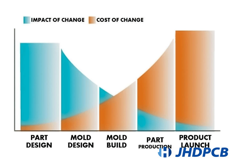
  • Enhancing Time-to-Market: Detecting and resolving manufacturing-related issues early in the design phase helps shorten the overall product development cycle. By addressing DFM considerations upfront, design iterations and rework caused by manufacturing issues can be minimized, enabling faster time-to-market.

In summary, a DFM inspection is crucial to ensure that a product’s design is compatible with the manufacturing processes and equipment. By identifying and addressing potential manufacturing issues early on, it helps improve product quality, reduce costs, and accelerate time-to-market.

What are the aspects of DFM inspection content?

Once you’ve completed a complex design and sent your data to your manufacturer, your design will be pored over by one or more engineers. These folks go through new designs looking for anything that could reduce fabrication and assembly yield, or that creates a risk of rework or a failed board. When you’re trying to get to market quickly, the last thing you need is for your board to receive no-bid status. Anything that appears as a discrepancy between design files, Gerber files, netlist data, and your BOM should be addressed before manufacturing. Some design choices can cause your board to receive no-bid status. Your new board won’t hit the fabrication line until all aspects of the design have passed these important checks and sign-offs are complete.
Before you send your board off for manufacturing, you should complete an in-house design review if you want to cut down the time required to put your board into production. The content of a DFM inspection can vary depending on the specific product and manufacturing processes involved. We’ve compiled a PCB DFM checklist that helps ensure your board will be fully manufacturable and testable. However, here are some common aspects that are typically considered during a DFM inspection:

  • Design Rule Check (DRC): A DRC is performed to verify whether the design meets the specified design rules and guidelines. This includes checking parameters such as trace widths, spacing, pad sizes, drill sizes, and other design constraints defined by the manufacturer or industry standards.
  • Component Placement: The inspection evaluates the component placement on the PCB layout to ensure that it is optimized for efficient assembly. This includes assessing component spacing, orientation, and accessibility for soldering or other assembly processes.
  • Assembly Process Compatibility: The DFM inspection considers the compatibility of the design with the intended assembly processes. It reviews the design for factors such as soldering techniques (e.g., surface mount or through-hole), solder mask requirements, stencil design, and any specific assembly guidelines provided by the manufacturer.
  • Design for Testability (DFT): The inspection assesses whether the design incorporates features that facilitate testing and troubleshooting during manufacturing. This may include the presence of test points, boundary scan capabilities, built-in self-test mechanisms, or other test-related features.
  • Thermal Considerations: The inspection examines the thermal aspects of the design, including proper heat dissipation and management. It looks for the presence of heat sinks, thermal vias, adequate spacing for airflow, and any other design elements that help prevent overheating or thermal issues.
  • Signal Integrity: The inspection evaluates the design for signal integrity concerns. This includes checking for proper impedance matching, controlled impedance routing, signal isolation, and noise reduction techniques to maintain signal quality and minimize electromagnetic interference (EMI) risks.
  • Design Documentation Review: The inspection involves a thorough review of the design documentation, including PCB layouts, schematics, assembly drawings, and any other relevant documentation. It ensures that the design is accurately documented and provides all the necessary information for manufacturing.
  • Design Cost Optimization: The inspection considers opportunities for cost optimization in the design. It looks for areas where design complexity can be reduced, material costs can be minimized, or manufacturing steps can be streamlined to achieve cost-effectiveness without compromising product quality.

It’s important to note that the specific content and depth of a DFM inspection may vary depending on the manufacturing processes, industry standards, and the expertise of the inspection team. The goal is to thoroughly evaluate the design for manufacturability and identify any potential issues that could impact the production process. After introducing some main inspections, here are some more detailed process inspection matters.

Apply DFM principles to PCB process list.

DFM (Design for Manufacturability) is a critical aspect of the PCB manufacturing process, ensuring that designs can be manufactured efficiently, cost-effectively, and with high quality. Next will explore the common basic principles of DFM in PCB production, covering aspects such as component placement, assembly, soldering, testing, and more. By following these principles, manufacturers can optimize the manufacturing process, reduce costs, and enhance the overall reliability of PCBs.

  • Minimum trace width and spacing: Select appropriate minimum trace width and spacing based on the manufacturer’s capabilities and requirements to ensure reliable manufacturing and good electrical performance.
  • Minimum hole size and pad diameter: Choose suitable minimum hole size and pad diameter to accommodate component leads and ensure proper solder joint formation.
  • Component orientation: Orient components on the PCB in a way that minimizes the need for complex or lengthy routing, reduces signal interference, and facilitates efficient assembly.
  • Copper balance: Maintain a balanced distribution of copper on the PCB to avoid excessive etching or plating issues. Ensure symmetrical copper traces and planes to promote uniform current flow and minimize impedance variations.
  • Panelization: Arrange multiple PCBs on a panel to optimize material usage, reduce production time, and facilitate automated assembly and testing processes. Consider appropriate breakaway tabs or mouse bites for easy separation.
  • Solder mask design: Design the solder mask to accurately define solderable areas and prevent solder bridging. Ensure adequate solder mask relief around pads and vias for proper solder flow.
  • Silkscreen placement: Place component designators, polarity indicators, and other markings on the silkscreen layer in a way that provides clear visibility without obscuring critical signal traces or pads. Click to learn more about PCB silk screen printing knowledge.
  • Tooling holes and fiducials: Include tooling holes and fiducial marks on the PCB to ensure accurate registration during assembly processes, such as pick-and-place and solder paste stencil alignment.
  • Routing considerations: Optimize routing to minimize signal crosstalk, impedance mismatches, and excessive signal reflections. Follow high-speed design guidelines for differential pairs, controlled impedance traces, and signal integrity.
  • Design for soldering processes: Consider the chosen soldering process (wave soldering, reflow soldering) and design the PCB layout to accommodate it. Ensure proper pad sizes, component spacing, and thermal relief for effective soldering and heat dissipation.

These specific DFM principles address various aspects of the PCB manufacturing process and can help optimize production efficiency, yield, and overall product quality.

Common DFM problems before PCB fabrication.

There are several common Design for Manufacturability (DFM) problems that can arise before printed circuit board (PCB) fabrication. Addressing these issues during the design phase can help prevent manufacturing challenges and ensure a smoother production process. Here are some common DFM problems to watch out for:

  1. Insufficient Clearances: Insufficient clearances between traces, pads, and other components can lead to short circuits during fabrication. It is important to adhere to design rules and guidelines regarding minimum clearances to prevent such issues.
  2. Inadequate Trace Widths: Inappropriate trace widths can cause problems during PCB fabrication, such as etching or plating difficulties. It is important to consider the current carrying capacity of the traces and adhere to recommended trace width guidelines.
  3. Unbalanced Copper Pour: Unbalanced copper pour or excessive copper distribution on one side of the PCB can cause warping or bowing during the fabrication process. It is essential to maintain a balanced copper distribution to ensure flatness and stability.
  4. Misaligned Drill Holes: Misaligned or off-center drill holes can cause issues during PCB fabrication and assembly. Properly aligning the drill holes with the corresponding pads and vias is crucial to ensure accurate drilling and component placement.
  5. Missing or Incorrect Footprints: Incorrect or missing component footprints can result in problems during assembly, such as misalignment, soldering issues, or poor electrical connections. It is important to verify and double-check the accuracy of component footprints in the design.
  6. Unsupported Manufacturing Processes: Designing features or elements that are not compatible with the chosen manufacturing processes can lead to fabrication difficulties or higher production costs. It is important to consider the capabilities and limitations of the manufacturing processes during the design phase.
  7. Lack of Design Documentation: Insufficient or inaccurate design documentation can cause confusion, delays, or errors during PCB fabrication. Properly documenting the design, including clear and detailed PCB layouts, schematics, assembly drawings, and manufacturing notes, is crucial for effective communication with the manufacturer.
  8. 90-degree bends in traces cause acid traps: to identify acid traps, it is necessary to know how the traces are positioned on the PCB surface. If the copper elements are bent less than 90 degrees (acute angle), they can act as acid traps during manufacturing. This occurs prior to cleaning as acid residue accumulates in this area and is not removed. The desired copper elements then begin to erode (over-etch) and an open circuit is formed. Since today’s plots are very thin (4 or 5 mils), it is very important to avoid acid traps. Therefore, avoid tracing at sharp angles. Try to maintain a 45° or 90° angle to the pitch.

    Avoid 90° bends

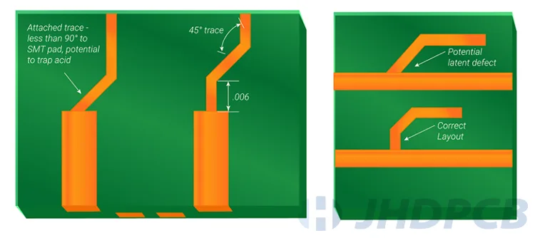
    Acid traps remove the desired copper feature, eventually creating an OPEN connection.

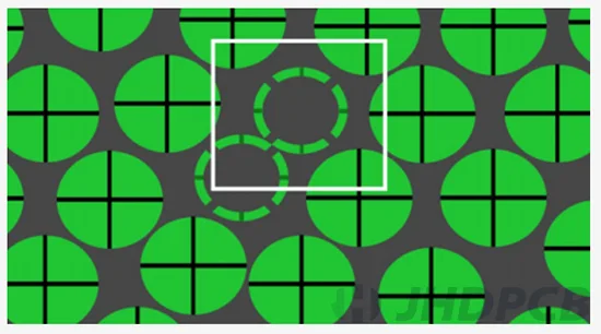
  9. Fluctuating copper pieces/solder mask create antennas: Splitters are small (conductive) copper wedges or (non-conductive) solder masks that float freely on a flat surface. They can adhere to other copper pieces or exposed copper and cause short circuits. If they are large enough to not float, they can also form antennas that can cause noise and other interference inside the board. Why does it become an antenna? Because it is not grounded and therefore acts as a signal pickup.
    How can copper debris be avoided? Copper debris can be avoided by keeping the copper properties at approximately 0.004″. In the example below, this is the distance between the anti-pads. While this trick is not completely foolproof, it greatly reduces the chance of copper being deposited elsewhere in the layer. It depends on the weight of the copper. The greater the weight of the copper, the greater the required connection area.

    Distance between anti-pads

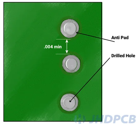
    Copper slivers can be avoided by maintaining the spacing between antipads around 0.004 inches.

  10. Thermal exhaustion leads to soldering problems: To provide sufficient heat for the soldering process, small copper bars are used on the heat dissipation pad. The bars prevent heat from being dissipated, ensuring a solid solder joint and an accurate electrical connection between the pad and the board. In some cases, voids between the heat and the plate or pad can result in an incomplete connection and minimize the heat concentration required for a proper connection. This can lead to a number of functional problems. Such thermals compromised by voids are referred to as stalled thermals. This can lead to uneven soldering and slow reflow times during the assembly process.

    Heat exhausted

    Starved thermals can affect the soldering process.

  11. The absence of a spacer on a pin causes a short circuit: pins (brought out through a hole) that have no spacers are connected to the plane. If a pin has no spacers on all levels, it connects to all voltage levels.
  12. Inadequate ring size causes circuit breakage: a hole size larger than the drill ring size is specified, which can cause the pin to break or short circuit at the same voltage level. For more pcb annular ring guidelines, please visit our blog.
  13. Copper too close to the edge of the PCB causes short circuits in adjacent layers: Sometimes the distance between the copper and the edge of the PCB is not sufficient. If the copper is too close to the edge, short circuits can occur between adjacent layers when current is applied to the board. This happens because of the exposed copper at the edge of the PCB. Addressing these common DFM problems before PCB fabrication through careful design review, adherence to design rules and guidelines, and collaboration with manufacturing experts can help prevent costly rework, delays, and yield issues in the production process. 

How to combine DFM in PCB production?

PCB designers need to consider the standards and constraints of PCB manufacturers to ensure a smooth design and manufacturing process; the Design for Manufacturing (DFM) process for PCB design must meet all requirements for PCB design. In this article, we will look at DFM best practices for PCBs. To effectively combine Design for Manufacturability (DFM) principles with PCB production, consider the following steps:

  • Involve Manufacturing Experts Early: Involve fabrication experts and professional PCB fabricators such as JHDPCB early in the design process. Working with a professional will provide valuable insight into manufacturing capabilities and limitations, allowing you to factor in DFM considerations from the start.
  • Understand Manufacturing Processes: Gain a thorough understanding of the PCB manufacturing processes involved, such as PCB fabrication, assembly, and testing. Familiarize yourself with the specific requirements, constraints, and recommended design guidelines for each process.
  • Follow Design Rules and Guidelines: Adhere to the design rules and guidelines provided by the manufacturer or industry standards. These rules specify design constraints for trace widths, spacing, pad sizes, drill sizes, and other critical parameters. Ensuring compliance with these pcb dfm rules reduces the risk of manufacturing issues.
  • Utilize DFM Tools and Software: Employ DFM check PCB tools and software that can automatically check your design for potential manufacturing issues. These tools can perform design rule checks (DRCs) and identify areas that may require optimization or modification to enhance manufacturability.
  • Optimize Component Selection: Choose components that are readily available, well-documented, and compatible with the chosen manufacturing processes. Verify component availability, lead times, and any specific requirements to ensure smooth procurement and assembly.
  • Perform Design Reviews: Conduct thorough design reviews, both internally and with manufacturing experts. Review the PCB layout, schematics, and assembly drawings to identify any potential manufacturing challenges. Address issues related to clearances, component placement, thermal management, signal integrity, and assembly process compatibility.
  • Design for Assembly (DFA): Optimize the design for efficient and accurate assembly. Consider factors such as component placement, orientation, and accessibility for soldering or other assembly processes. Ensure that the design facilitates automated assembly techniques whenever possible.
  • Implement Design for Testability (DFT) Features: Incorporate DFT features to facilitate testing and troubleshooting during manufacturing. Include test points, boundary scan capabilities, built-in self-test mechanisms, or other test-related features to simplify the testing process and improve overall product quality.
  • Validate the Design: Before finalizing the design, perform design validation by using simulation tools or prototyping. This helps identify and resolve any remaining manufacturing issues, ensuring that the design is optimized for production.
  • Maintain Communication with Manufacturers: Maintain communication with PCB manufacturer (JHDPCB) and assembly house throughout the production process. Seek advice and guidance from our expert engineers on manufacturability issues and resolve any issues promptly.

By combining these steps, you can integrate DFM principles into the PCB production process, resulting in a design that is optimized for efficient manufacturing, improved yield rates, reduced costs, and enhanced overall product quality.

How to achieve good DFM with PCB design tools?

Achieving good Design for Manufacturability (DFM) with PCB design tools involves utilizing the features and capabilities of the software to optimize your design for efficient and reliable manufacturing. Here are some steps to achieve good DFM using PCB design tools:

  • Select a DFM-Oriented Design Tool: Choose a PCB design tool that incorporates DFM features and functionality. Look for tools that provide design rule checking (DRC), design for assembly (DFA), and design for testability (DFT) capabilities. These features help identify potential manufacturing issues and guide you towards DFM-compliant designs.
  • Familiarize Yourself with Design Rules: Understand the design rules and guidelines provided by your PCB fabricator or industry standards. Configure the design rule settings within the PCB design tool to match the specific DFM requirements. This ensures that your design is checked against the appropriate manufacturing constraints during the design process.
  • Utilize Design Rule Checking (DRC): Use the DRC feature of the PCB design tool to automatically check your design against the specified design rules and guidelines. DRC verifies parameters such as trace widths, clearances, pad sizes, and drill hole specifications. Fix any DFM violations highlighted by the DRC to ensure compliance with manufacturing requirements.
  • Optimize Component Placement: Use the PCB design tool’s placement features to optimize component placement for efficient assembly. Consider factors such as proximity of components, alignment of pads, and accessibility for soldering or other assembly processes. Utilize automated placement and routing features to achieve an optimal layout that adheres to DFM guidelines.
  • Employ Design Rule Constraints: Leverage the design rule constraint features provided by the PCB design tool. Define and enforce design rules for trace widths, clearances, thermal considerations, and other critical parameters. Setting up and enforcing these constraints helps maintain DFM compliance and prevents potential manufacturing issues.
  • Perform Design Validation and Simulation: Use the simulation capabilities of the PCB design tool to validate the design’s performance and manufacturability. Perform signal integrity analysis, thermal analysis, dfm analysis and other simulations to identify potential issues and optimize the design accordingly. This helps ensure that the design meets manufacturing requirements and functions as intended.
  • Generate Accurate Manufacturing Outputs: Utilize the manufacturing output generation capabilities of the PCB design tool to produce accurate and comprehensive manufacturing documentation. This includes generating Gerber files, drill files, assembly drawings, and other manufacturing-related outputs required by the fabricator. Double-check the generated outputs to ensure they align with the intended DFM specifications.
  • Stay Updated with Software Updates: Regularly update your PCB design tool to benefit from the latest DFM features, bug fixes, and performance enhancements. Stay informed about new DFM-related functionalities introduced in software updates and utilize them to improve the manufacturability of your designs.

Remember that while PCB design tools provide DFM features, it’s essential to collaborate with manufacturing experts and fabricators throughout the design process. Their expertise and guidance can further enhance the DFM aspects of your design and ensure its compatibility with the specific manufacturing processes.

JHDPCB assists free PCB fabrication DFM file check.

Design for Manufacturability (DFM) is critical in ensuring efficient and reliable PCB production. By considering manufacturing requirements and constraints during the design phase, potential issues can be identified and addressed, resulting in improved product quality, cost reduction, and faster time-to-market. Achieving good DFM with PCB design tools involves utilizing their features, such as design rule checking, simulation, and design optimization, to create designs that adhere to manufacturing guidelines.
At JHD, our engineers have a wealth of experience and expertise. Our team conducts preliminary DFM design checks early in the order process to improve production efficiency and quality.
Our engineer team has the following advantages:

  • Manufacturing Process Familiarity: We have in-depth knowledge of various PCB manufacturing processes, including fabrication, assembly, and testing. This enables us to accurately assess the manufacturability of designs and fully leverage DFM principles.
  • Effective Use of DFM Tools: We utilize advanced PCB design tools that encompass design rule checking, simulation, and optimization capabilities. Through these tools, we proactively prevent potential manufacturing issues and refine design solutions.
  • Continuous Learning and Updates: Our design team is constantly on the lookout for the latest DFM trends, techniques and tools. Continuously improve our professional capabilities to adapt to the ever-changing manufacturing environment and requirements.

If you are developing a new PCB, you should check all factors early in the design process. Of course, even if your PCB project is in production, you can check and change it.
A lot of ideas, time and energy are invested in DFM. Senior product development engineers in JHDPCB have extensive experience in product development, design and manufacturing. We will cooperate with you to conduct a free DFM inspection. We are committed to partnering with our clients to develop manufacturable solutions that meet their needs. 

Get a PCB Quote Now

Open high-quality PCB manufacturing services in JHDPCB

Explore more JHDPCB blogs

Leave a Comment