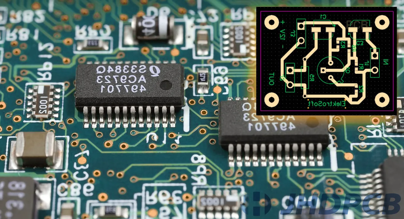

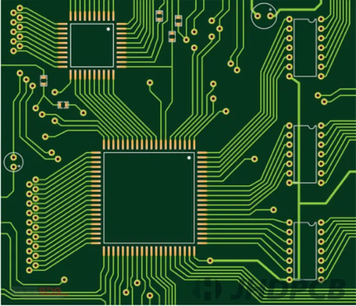
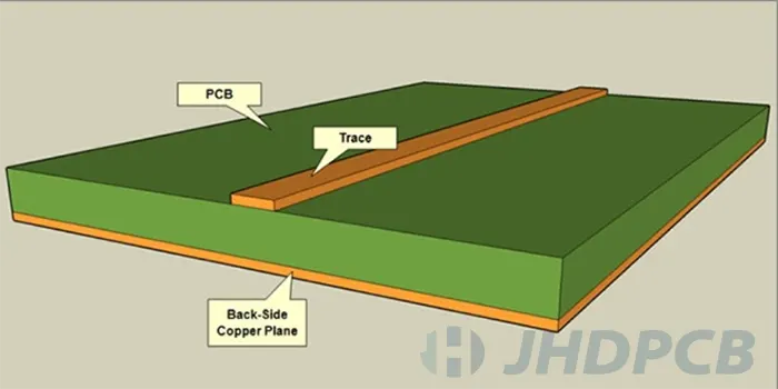
PCB trace is the track that signals and data travel during printed circuit board operation, which is of great importance to the printed circuit board. It connects different components together to ensure the normal functioning of the printed circuit board. The signal conducted by the trace is composed of electricity, which requires the material making the trace to have high conductivity and stability. The circuit board trace refers to the routing network, fuses, insulation, and copper that make up the PCB. Thereinto, the most common material is copper. PCB copper trace can guarantee the operation of printed circuit board through its good conductivity and relative stability.
Every substance in nature has a certain resistance to current, so both conductors and insulators will produce varying degrees of obstruction to the passage of current. In the fabrication of PCB track, copper is a common conductor material, but due to the composition and properties of copper itself, it will still cause resistance to the current, which is PCB track resistance.
In a circuit, resistance is measured in ohms and is an indicator to measure current resistance. PCB trace resistance is commonly used to determine the signal transmission loss through the PCB, in addition to measuring the power that the trace can consume. Again, the trace resistance value must be low enough to allow the current to pass through the PCB circuit. It depends on the trace’s thickness, width and length, and is a key factor that should be calculated and analyzed during PCB design.
Tracking resistors mainly face the problem of power loss, which can lead to temperature increase and conductivity decrease. The most effective way to solve the power loss caused by tracking resistance is to increase the tracking area, which is closely related to width and thickness. Precise width and thickness can reduce heat accumulation. The wider the trace, the less resistance it has to the current, and the less heat it accumulates. There are plentiful methods can be used to reduce resistance, such as choosing thicker layers of copper or increasing the area of copper used. The demand point of thick copper PCB comes from this.
![]()
Ohm’s law to show the relationship between the resistance is inversely proportional to the current, resistance expressed as 𝑅 = 𝑉 / 𝐼, where R is the total resistance, V represents the circuit voltage, I refer to the current in the circuit. This means that the lower the resistance, the higher the current. In addition, according to the 𝑃 = 𝑉 𝐼 can be concluded that the current is proportional to the power relationship. Where P is the power, V is the applied voltage, I is the circuit current. These two formulas can help to understand the basic relationship between different parameters.
The calculation formula of PCB track resistance is:
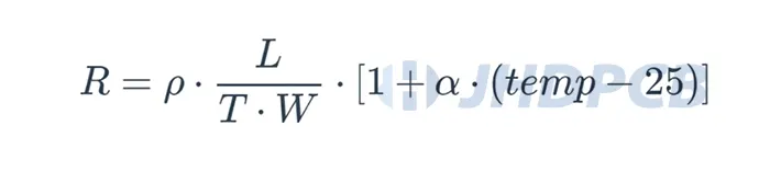
Thereinto, L is the length of the track, W is the width, T is the thickness, and α is the temperature coefficient of copper.
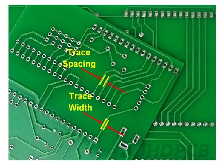
PCB trace width, measured in mils or thousands of inches, is an important parameter in PCB design. Common signals have trace widths ranging from 7 to 12 mils (JHD can be adapted and adjusted according to PCB design requirements and application current overload capacity) and lengths up to several inches. However, when setting the width and length of the track, it is necessary to consider many factors such as PCB trace spacing and PCB trace ampacity. In addition, in the design, but also must be with the manufacturing cost, board density and size and performance and other aspects of adaptation. If there are specific requirements for things like noise control or speed, then the width of the trace is a priority, even more so than manufacturing cost, board size and other factors.
Thickness has a great impact on the PCB in maintaining the balance. Whether the PCB maintains the balance will affect its functional performance status. Generally, PCB trace thickness ranges from 0.008 Inch to 0.240 Inch (JHD can be adapted and adjusted according to PCB design requirements and application current overload capacity), and it must be consistent throughout the PCB. There are a wide variety of PCB boards on the market, including single panel, double panel and multilayer board. The thickness of the track also varies according to the structure and type of the circuit board.
Both standard trace width PCB and PCB trace thickness play a crucial role in PCB design, as they determine the amount of electricity that can pass through the circuit trace without overheating and damaging the board. In addition, a circuit trace with a large cross-sectional area helps to handle higher power. If the width and thickness are not taken seriously, the PCB board will not work properly, and even lead to overheating or damage of the circuit trace, which will destroy the PCB board connected to the components. A properly calibrated PCB routing width and thickness helps to minimize the heat build-up in the circuit board. The wider the trace, the lower the resistance to the current, and the less the heat accumulation.
Many factors will affect the width and thickness of the track, such as:
- Capacitance of pcb trace – the rated current-carrying capacity of the product design;
- Cross-sectional area of the trace- More powerful equipment requires a larger cross-sectional area of the trace;
- Impedance control – the circuit impedance between the laminate and the traceis controlled within the rated range to ensure the integrity of signal transmission;
- Locus location – may be in the top, bottom, or middle layers;
- The larger the length – width and height of the trace, the higher the current needs to be carried by the trace, and its ultra-high resistance value will lead to greater power loss. The generated heat will directly affect the service life of PCB;
- The thickness of the copper layer- the default is usually 1oz to 2oz;
- The cross section of the tracethe cross section area-the higher the power, the greater the cross-sectional area requirement;
- The location layout of the trace.
The design and layout of the printed circuit board is closely related to the production cost and use efficiency of the circuit board. The reasonable layout design can not only save the production cost, but also make the circuit board operate efficiently. If you do not pay attention to the layout, it may produce electromagnetic interference, circuit failure and other serious problems. In the layout, the practical problems should be fully taken into account, such as the quality of materials and components, component placement, power and heat problems, and circuit board limitations, so as to make the layout more reasonable and maximize its working efficiency.

PCB trace spacing and pcb trace width will affect the circuit board through various forms, so we need to focus on the following four factors:
- Electrical performance and signal integrity-
In general, most tracks on the board default to certain values for width and spacing. However, there are cases where different dimensional widths or spacing are required. For example, controlled impedance networks require the pcb trace width to be calculated in a configuration where the board layers are stacked. Sensitive and high-speed traces require spacing values large enough to prevent signal crosstalk. Because of the differences in the uses of circuits, there may be special requirements for the width and spacing of traces. For instance, the default PCB trace width will be reduced in narrow areas. - Power and Ground Routing-
In order to transmit more current, the path to the power source or ground should be wider. Too thin trace is easy to heat, when the high power of the current through easy to burn through. In addition, the inside of the board should have a wider wiring path than the outside, to speed up heat dissipation. At the same time, in order to reduce the noise in the circuit, the trace in the circuit board should be as short as possible. If the tracks need to carry a large current, the spacing between them should be properly widened, otherwise the traces will be prone to arc. - Fabrication of circuit board-
Compared with only 3 mil traces, 20 mil traces have larger metal loss tolerance, which indicates that the larger the PCB trace width, the more favorable the fabrication of circuit boards. The weight of copper used in circuit board fabrication has a great influence on the track width. If the weight of copper is too large, it is difficult to carve a thin track width on the circuit board. Thus, the design of pcb copper trace cannot be ignored. - Circuit board assembly-
Welding is adversely affected if PCB trace width is too wide. If PCB trace width is too wide for ground grids and power supplies, uneven heating and welding point blockage may occur.
Before design, the first thing you need to do is determining the pcb trace design rules, and then understand the manufacturer’s specifications and power distribution in detail. Remember not to rush to use automatic add-ons.
During the design, a reasonable and sufficient track width should be set, the through hole needed to be used to conduct heat, again, a certain space should be reserved between the track and the mounting hole. At the same time, the grids are supposed to be properly spaced, and don’t have too many grids. In addition, noise should be reduced as much as possible.
After design, it is necessary to strictly check the design content for many times, and test the experimental product repeatedly according to the design method, in order to ensure the safety of the circuit board and ensure its normal operation.
In the design process, there are the following aspects to pay attention to:
Choice of routing type
Wiring can be divided into manual wiring and automatic wiring, among which automatic wiring is the inherent function of PCB design software. Designers cannot completely rely on the function of automatic wiring, because the function can not replace manual wiring to play the designer’s creativity and flexibility, it can only be used as a tool to save time.
The selecting of PCB trace width
PCB trace width is important for the operation of the circuit. PCB trace width must be appropriate to the capacitance of pcb trace to ensure the smooth passage of current. The minimum width of the pcb trace needs to be determined precisely, otherwise the circuit board could overheat, which is a matter of heat management and performance.
Ensure that the analog track and the digital track are separated
Generally, digital signals are transmitted through parallel trace. If the digital trace and analog traces are arranged together, it is easy to generate signal interference and thus generate noise. Therefore, especially at high frequencies, the trajectory carrying the digital signal must be separated from the trace carrying the analog signal.
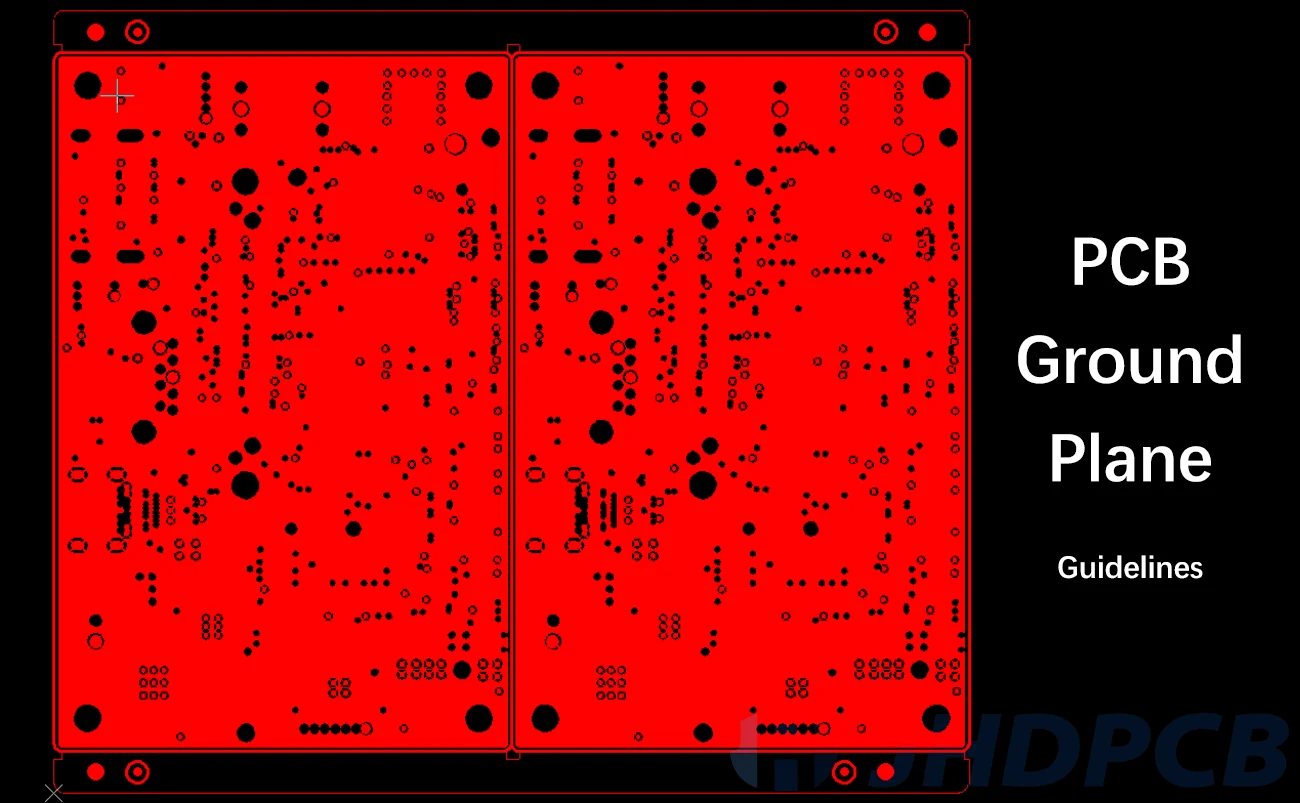
Connect to the ground plane
Each individual pcb trace needs to be connected to the ground plane rather than the ground, because the ground plane provides the same reference point for all tracks to measure voltage. On the contrary, if connected to different ground, will get different voltage and resistance. Therefore, a solid ground plane should be established and placed below the path carrying the signal, which may improve its resistance to noise while reducing the impedance. In addition, power and ground planes can be placed in the innermost layer of the board to prevent distortion or separation of components due to the bending of the board.
Provide adequate spacing and space between components
Leaving a gap of 0.007 to 0.0010 inches between adjacent tracks and pads can prevent short circuits during the manufacturing or assembly phase of the PCB. Likewise, enough space is needed around the mounting holes to prevent electric shock.
Alternate the direction of PCB trace
If most of the traces on a certain plane are oriented in the same direction, the PCB traces on adjacent planes should be oriented in another direction perpendicular to it, thus reducing the risk of crosstalk between traces.
Avoid capacitive coupling
Placing PCB traces configured for the power supply and analog signals on a dedicated plane can reduce the capacitive coupling caused by the tracks above and below the ground. In addition, decoupling capacitors can also reduce the occurrence of capacitive coupling, which is a practical and affordable component.
Layout of thermal vias and pads
The use of hot pads on the through-hole assembly can improve the heat dissipation capacity while making the welding simpler. In addition to hot pads, hot through holes also play a vital role because they can be electrically connected between layers and are able to transfer heat from the hottest components to the outside for heat dissipation.
Thickness of the ground trace and the power supply trace
To allow greater current passage, trajectories to the power and ground need to be thicker. They can be easily detected even by the naked eye, which can reduce the occurrence of misconnections. In general, the normal trace is 0.025 inches wide, while the ground trace and the power supply traces are 0.04 inches wide.
Avoid right Angle
At high frequencies, rectangular curves tend to increase the risk of crosstalk, radiation and reflection, resulting in discontinuity of the signal, and thus damage the integrity of the signal.
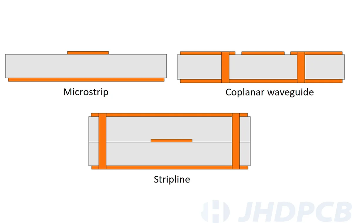
Transmission line type
There are different transmission line types on printed circuit boards, and selecting the appropriate transmission line type can provide targeted impedance control. to ensure equipment performance. There are three common transmission types of PCB: microstrip line, stripline and coplanar waveguide. Detailed information can be learned on our corresponding page.
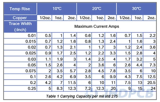
In addition to the calculator, the PCB track width table is also a convenient tool. It shows the amount of electricity a trace can carry, as well as the effect of temperature rise, and can be used to quickly determine the pcb trace width.
- The first step is to calculate Area:
It is possible that the region[mils^2] = (Current[Amps]/(k*(Temp_Rise[deg. B])^b))^(1/c) - Next, Width is computed.
Width[mils]=Area[mils^2]/(Thickness[oz]*1.378[mils/oz])
Internal layers of the For IPC-2221 model: k = 0.024, b = 0.44, c = 0.725
For IPC ϭ 2221 outer layers: k = 0.048, b = 0.44, c = 0.725
where k, b and c are constants resulting from fitting the curves to the IPC 2221 curves.
Learning about how to fix pcb trace is also important. When the power supply unit has problems such as display failure and strange noise, it is a sign that the pcb trace needs to be repaired. Before maintenance, it is necessary to determine the resistance and the pcb trace width through measurement and other ways. During the repair process, you need to consider the maximum current that the circuit board can accept. When the current is too large, there may be short circuit and other conditions.
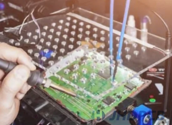
Specific maintenance steps are as follows:
- First find the damaged trace.
When a damaged trace is found, it should be removed with a cutting tool, and care should be taken not to damage the surrounding parts. - Clean the damaged marks to a copper color and tin the exposed areas.
Clean the repair area with a cleaning paper towel or a solvent cleaning pen. At this point, the existing track can be coated with flux, and a soldering iron can be used to assist the solder wire in tinning both sections of the track. - Select a new wire that can replace the old one.
Ensure that the new wire is in good condition and of the right size to replace the original wire. - Tin the ends of the jumper wire.
If the new wire is suitable, remove the insulation from both ends and weld with solder. - Weld one end of the wire.
A section of the new wire is overlapped with the existing trace by more than twice the pcb trace width. After fixing the wire with tape, apply flux on the overlap, and then the wire and the trace will be welded together. - Flexible wire formation according to specific needs and requirements.
- Attach the wire to the surface of the circuit board.
During this process, tools such as tape and adhesive can be used to keep the wires firmly attached to the circuit board. - Finally weld the other end of the wire.
Repair is basically completed after welding, and don’t forget to clean residual stains after checking to ensure that the connection is normal.