PCB Trace Spacing

Trace Spacing: A Guide for PCB Design

directory

The formulation of printed circuit boards (PCBs) is a pivotal element in the development of electronic products. A key consideration in PCB design is ensuring proper trace spacing, which refers to the distance between conductive elements, such as traces and pads, on the PCB. Trace spacing plays a critical role in maintaining signal integrity, minimizing crosstalk, and avoiding potential short circuits.
In this document, we will explore the principles of PCB design of trace spacing, including industry standards and best practices. We will discuss various factors that influence trace spacing requirements, such as voltage levels, signal frequencies, environmental conditions, and manufacturing processes. Additionally, we will cover specific applications, such as high-speed digital designs and power distribution systems, where trace spacing requirements are particularly important.
Through this document, engineers and designers can gain a comprehensive understanding of PCB design of trace spacing, enabling them to produce high-quality PCB designs that meet the required performance and safety standards. By implementing the appropriate trace spacing guidelines and design principles, designers can ensure reliable operation, minimize signal distortions, and mitigate potential risks associated with inadequate trace spacing.

What is PCB Trace/Line Spacing?

PCB trace or line spacing refers to the distance between two adjacent traces or lines on a printed circuit board. It refers to the space or distance between the conductive traces on the printed circuit board (PCB). The spacing is important to prevent electrical interference, crosstalk, and short circuits between adjacent traces.
The gap between the traces on the PCB is influenced by multiple factors, such as the voltage levels, signal frequencies, and the manufacturing capabilities of the PCB fabrication process. Higher voltage levels and frequencies generally require larger spacing to avoid electrical breakdown or signal interference.

PCB manufacturers often provide design guidelines or specifications for trace spacing based on their manufacturing capabilities and industry standards. These pcb trace spacing guidelines ensure that the PCB design meets the required electrical and safety standards.
Designers must consider the trace spacing along with other design parameters, such as trace width, impedance control, and signal integrity requirements, to ensure proper functioning and reliability of the printed circuit board.

The Standards of Regulating PCB Trace Spacing.

The standards for regulating PCB trace spacing are defined by various industry organizations and standards bodies. These standards ensure that the spacing between traces on a printed circuit board (PCB) meets certain requirements to prevent signal interference, electrical leakage, and other issues. Here are several important criteria that govern the spacing of traces on a printed circuit board (PCB):
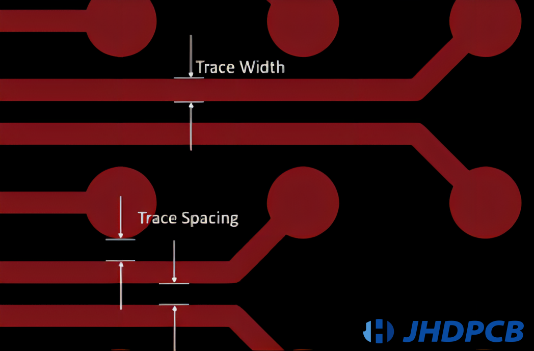
criteria that govern the spacing of traces

  • This standard provides guidelines for PCB design, including trace spacing. PCBs are classified into three categories according to their intended uses: Class 1 (for general electronic products), Class 2 (for dedicated service electronic products), and Class 3 (for high reliability electronic products).
  • For Class 2 and 3 PCBs, the standard recommends a minimum trace-to-trace spacing of 0.25mm (10 mil) for low voltage and 0.5mm (20 mil) for high voltage. These values represent the minimum PCB trace spacing, also known as the pcb minimum trace spacing, required to ensure safe operation and prevent breakdown.
  • For Class 3 PCBs, the standard also specifies minimum creepage and clearance distances between conductors to prevent electrical leakage, with values ranging from 0.1mm (4 mil) to 2mm (80 mil) depending on the operating voltage.
    Read more about the IPC class standard definitions for PCB manufacturing.
  • This updated version of IPC-2221 addresses challenges related to high-speed digital and high-frequency analog PCB designs. It offers more specific guidelines regarding trace spacing to ensure signal integrity and mitigate electromagnetic interference.
  • For example, for high-speed digital signals with a rise time of 1ns or less, the standard recommends a minimum differential trace spacing of at least 3H, where H is the distance between the trace and a plane or reference plane.
  • The standard also suggests different trace spacing requirements for different signal frequencies, with higher frequencies requiring tighter spacing to prevent crosstalk and signal distortion.
  • This standard focuses on the mechanical design requirements for PCBs, including trace spacing. It provides guidelines for determining the minimum spacing between traces based on factors such as voltage levels, current carrying capacity, and environmental conditions.
  • For example, for low-voltage PCBs (<50V), the standard recommends a minimum trace-to-trace spacing of 0.25mm (10 mil) for Class 1 and 2 PCBs, and 0.15mm (6 mil) for Class 3 PCBs.
  • The standard also specifies minimum spacing requirements between different types of conductors, components, and edges to prevent accidental contact and ensure safety.
  • This safety standard specifies the minimum spacing requirements for PCB traces to prevent electrical arcs and short circuits. The specifications differ depending on the type of conductors and voltage levels used.
  • For example, for low-voltage conductors (<30V), the standard requires a minimum spacing of 0.8mm (32 mil) between uninsulated conductors and 1.6mm (64 mil) between insulated and grounded conductors.
  • For higher voltage levels (>250V), the standard specifies larger minimum spacing requirements between different types of conductors and between conductors and other parts of the PCB assembly.
  • This standard provides guidelines for designing high-speed digital systems, including PCBs. It covers topics such as signal integrity, power distribution, and trace spacing to ensure reliable operation of high-speed circuits.
  • For example, for differential signals with a rise time of less than 1ns, the standard recommends a minimum differential spacing of at least 3H to prevent crosstalk.
  • The standard also provides specific recommendations for the spacing between power and ground planes to minimize the impedance of the power distribution network.
  • The standard specifies a minimum spacing of 0.25mm (10 mil) between pads and traces for Class 1 and 2 PCBs, and 0.18mm (7 mil) for Class 3 PCBs.
  • It recommends a minimum spacing of 1.5mm (60 mil) between components and adjacent traces to prevent heat transfer issues during soldering.
  • The standard also provides specific guidelines for the spacing between through-hole components and SMT components to ensure proper assembly.
  • The standard specifies a minimum spacing of 0.25mm (10 mil) for Class 1 and 2 PCBs, and 0.15mm (6 mil) for Class 3 PCBs, between traces carrying voltages up to 50V.
  • For higher voltage levels, it recommends increasing the spacing requirements based on the insulation requirements and operating environment.
  • The standard provides different spacing requirements for different types of conductors, such as power and signal traces, and for different layers of the PCB stackup.
  • The standard specifies a minimum clearance distance of 2.5mm (0.1 inch) between patient connections and other conductive parts of the equipment.
  • It recommends a minimum spacing of 4mm (0.16 inch) between power supply components and high-voltage circuits to prevent electrical arcing.
  • The standard also provides specific guidelines for the spacing between PCB components and traces to avoid electromagnetic interference and ensure reliable operation.

These are just a few examples of the guidelines and recommendations provided by each of these standards. PCB designers and manufacturers must carefully consider the specific requirements of their applications and consult the relevant standards to ensure that their PCB designs meet the required performance and safety criteria.

Why are Trace Spacing Design rules crucial in circuit design?

Trace Spacing Design rules crucial in circuit design

There are several key points that highlight the significance of Trace Spacing Design rules in electronic circuit design. Understanding these points can help emphasize the importance of adhering to these guidelines for optimal performance and reliability.

  1. Electrical Safety: By maintaining suitable trace spacing, it becomes possible to avoid arcing between high voltage traces, thus guaranteeing circuit safety and decreasing the probability of electrical hazards.
  2. Signal Integrity: Adequate spacing between traces reduces crosstalk, minimizing the interference between signals and maintaining signal integrity. This is crucial for high-speed digital and analog circuits.
  3. Impedance Control: By following trace spacing design rules, designers can achieve the desired impedance for transmission lines, ensuring optimal signal quality and reducing reflections.
  4. Manufacturing Reliability: Design rules for trace spacing take into account the capabilities and tolerances of the PCB fabrication process. Following these guidelines guarantees the precise and dependable manufacture of the PCB, thereby decreasing the possibility of manufacturing defects.
  5. EMI/EMC Compliance: Proper trace spacing helps in minimizing electromagnetic interference (EMI) and achieving electromagnetic compatibility (EMC) compliance. This is especially important for circuits operating in sensitive environments or those requiring regulatory compliance.
  6. Heat Dissipation: Adequate spacing between power traces and other components helps in efficient heat dissipation, preventing thermal issues and ensuring the reliability of the circuit.
  7. Design for Manufacturing (DFM): Following trace spacing design rules simplifies the manufacturing process by reducing the chances of short circuits, opens, or other manufacturing-related issues. This leads to cost-effective and efficient PCB production.
  8. Design for Testability (DFT): Proper trace spacing allows for easier probing and testing of the PCB during the manufacturing and debugging stages, improving testability and reducing the time required for troubleshooting.
  9. Design for Serviceability: Adequate spacing between traces makes it easier to access and repair components on the PCB, enhancing the serviceability and maintenance of the circuit.
  10. Design Consistency: Following trace spacing design rules ensures consistency in PCB layout, making it easier for multiple designers or teams to collaborate on a project and reducing the chances of errors or inconsistencies.

In summary, adhering to trace spacing design rules is crucial for ensuring electrical safety, signal integrity, impedance control, manufacturing reliability, EMI/EMC compliance, heat dissipation, DFM, DFT, serviceability, and design consistency in PCB design.

What is the rule of Trace Spacing Design?

The trace spacing design rules can vary based on different factors, such as voltage, impedance, crosstalk prevention, manufacturability, and safety margin. Let’s dive into each of these factors:

1.Based on Voltage:
The minimum spacing between traces is determined by the voltage difference between them. Increased trace spacing is necessary for high voltage traces to prevent electrical breakdown and arcing. The following table provides common design rules based on trace-to-trace voltage:

Trace-to-Trace VoltageMinimum Spacing
< 50V2x trace width
50-150V3x-4x trace width
150-300V5x-8x trace width
>300V10x+ trace width

2.Based on Impedance:
Trace spacing can also be influenced by the desired impedance for high-speed signal integrity. Widening the spacing between traces lowers capacitive coupling, thereby increasing impedance. The following examples illustrate design rules based on target impedance:

Target ImpedanceSpacing
50 Ohms1x-2x trace width
75 Ohms2x-3x trace width
90-100 Ohms3x-4x trace width

3.Based on Crosstalk Prevention:
Crosstalk refers to unwanted interference between adjacent traces. To minimize noise coupling, recommended pcb trace spacing, i.e., larger spacings are recommended for high-speed digital or analog traces. This is because high-speed signals can create electromagnetic interference (EMI) and crosstalk, which can cause signal degradation or even loss of data. Increasing the distance between these traces can reduce the effects of EMI and crosstalk by increasing the isolation between them. The spacing requirements vary based on the type of trace:Target ImpedanceSpacin

Signal TypeSpacing
Digital signals > 50MHz>4x trace width
RF/microwave traces>5x trace width
Sensitive analog signals>3x trace width

4.Based on Manufacturability:
Trace spacing should consider the fabrication process capabilities and tolerances to ensure manufacturability. Different PCB technologies and layer configurations have specific minimum spacing requirements. Here are some typical values:

PCB TechnologyMinimum Spacing
>6 layer board5 mils
2-6 layer board6 mils
Doubleside board8 mils
Thick copper boards>10 mils

5.Based on EMI/EMC Considerations:
Electromagnetic interference (EMI) and electromagnetic compatibility (EMC) are crucial factors in modern electronic designs. Proper trace spacing can help reduce EMI emissions and enhance EMC performance. Higher-frequency signals and sensitive components may require larger spacing to mitigate EMI/EMC issues.

Signal TypeSpacing
High-Frequency Signals>4x trace width (frequency-dependent)
Sensitive Components>2x-3x trace width (component sensitivity-dependent)

6.Based on Thermal Considerations:
Trace spacing can also be influenced by thermal considerations to ensure proper heat dissipation and prevent overheating of adjacent traces. The following design rules illustrate the spacing for thermal considerations:

Trace TypeSpacing
High Current3x-4x trace width
Power4x-5x trace width

7.Based on Differential Pairs:
Differential pairs are commonly used for transmitting high-speed signals with low noise and crosstalk. The spacing between the two traces of a differential pair should be tightly controlled to maintain signal integrity and match impedance.

  • Differential Pairs Spacing: 0.1x-0.3x trace width, depending on the design requirements.

8.Based on Environmental Factors:
If the PCB will be exposed to harsh environmental conditions such as temperature extremes or high humidity, greater trace spacing may be necessary to ensure reliability and prevent potential failures caused by environmental stress.

  • Harsh Environment Spacing: >2x-3x trace width, depending on the severity of the environment.

9.Safety Margin:
Adding a safety margin to the trace spacing accounts for process variability and reduces the risk of shorts during manufacturing. The amount of margin can vary depending on the application stage (prototyping or production). A suggested practice is to allocate an additional 10-20% space for margin when it comes to spacing.

10.Based on Signal Ground Separation:
For designs carrying both high-speed signals and analog signals, it is vital to separate signal ground planes from each other. The size of the separation regions should be at least twice the width of the power or signal trace.

11.Based on Trace Routing:
Trace routing can also affect spacing requirements. In situations where traces are routed parallel to each other, additional spacing may be required to prevent crosstalk. For instance, when traces are routed in a meander pattern, the spacing can be increased to three times the trace width.

Overall, these guidelines provide a comprehensive approach to trace spacing design rules that ensure reliable and robust PCB layouts. Designers must carefully consider these design rules during the PCB layout process to achieve optimal performance and prevent potential problems such as crosstalk, arcing, and electrical breakdown.

Specific applications

High-speed digital designs:
In high-speed digital designs, trace spacing requirements are crucial to ensure signal integrity and minimize electromagnetic interference (EMI). As signal frequencies increase, it becomes necessary to maintain proper spacing between traces to prevent signal crosstalk and impedance discontinuities.
To meet these requirements, industry standards such as IPC-2221 and IPC-2223 provide guidelines for minimum trace spacing based on factors like signal frequency, rise time, and the type of material used for PCB fabrication. Designers should also consider controlled impedance routing techniques, such as differential pair routing and careful layer stackup planning, to minimize signal reflections and maintain signal integrity.

Power distribution systems:
In power distribution systems, voltage pcb spacing trace requirements are essential to prevent electrical arcing and ensure proper insulation between high-voltage traces. High-voltage traces require larger spacing compared to low-voltage traces to avoid potential short circuits and electrical breakdown.
Industry standards like IPC-2221 and IPC-2223 provide guidelines for minimum creepage and clearance distances for different voltage levels. Creepage distance indicates the minimum route along the PCB surface connecting two conductive elements, while clearance distance denotes the minimum distance through air or solid insulation material separating two conductive elements.
Designers must consider these spacing requirements when designing power distribution systems to ensure safety and compliance with regulatory standards.
In general, the trace spacing criteria differ based on the particular application and its related variables. By following industry standards and best practices, PCB designers can ensure proper trace spacing to achieve optimal performance, signal integrity, and safety in their designs.

How to calculate proper pcb trace spacing for various voltage levels?

calculate proper pcb trace spacing for various voltage levels

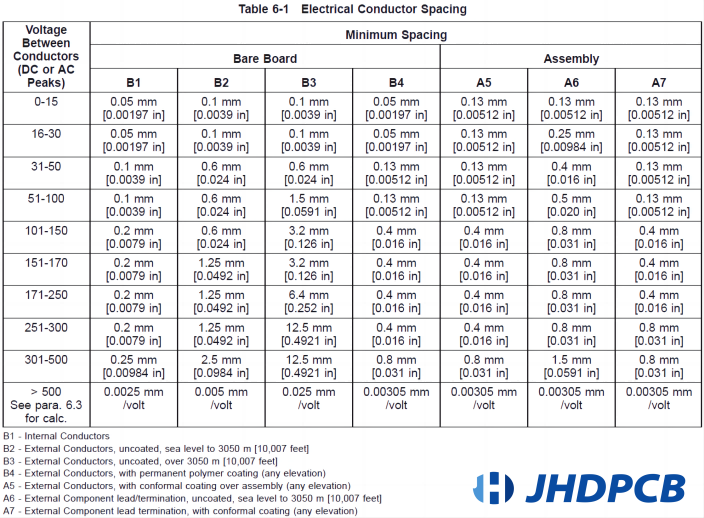
To calculate the proper PCB (Printed Circuit Board) trace spacing for various voltage levels, you can use a PCB trace spacing calculator. However, it is important to consider several factors such as the dielectric breakdown strength of the PCB material and the required clearance based on safety regulations. Here is a general guideline for calculating the trace spacing:

  1. Determine the required clearance: The required clearance is usually specified by safety regulations or industry standards such as IPC-2221. It defines the minimum distance required between conductive traces or between traces and other components to ensure electrical safety and prevent arcing or breakdown. Refer to the applicable standard for the required clearance values based on the voltage levels involved.
  2. Determine the dielectric breakdown strength: The PCB material used in the design has a specific dielectric breakdown strength, which indicates the maximum voltage the material can withstand before it breaks down. Consult the datasheet or manufacturer specifications to find the dielectric breakdown strength of the PCB material.
  3. Calculate the trace spacing: Once you have the required clearance and the dielectric breakdown strength, you can calculate the trace spacing using the formula:

     Trace Spacing = Required Clearance + (Dielectric Breakdown Strength / Voltage Level)

    The required clearance and dielectric breakdown strength are expressed in the same units (e.g., mm), while the voltage level is expressed in volts. The resulting trace spacing value is the minimum distance between conductive traces or between traces and other components that must be maintained to ensure electrical safety and prevent breakdown. The trace spacing calculation can be adjusted for different voltage levels by adjusting the value of Voltage Level in the formula.

    For example, let’s say the required clearance is 0.2mm and the PCB material has a dielectric breakdown strength of 40kV/mm. If you are working with a voltage level of 12V, the trace spacing would be:

     Trace Spacing = 0.2mm + (40kV/mm / 12V) = 0.2mm + 3.33mm = 3.53mm

    In this example, you would need to maintain a trace spacing of at least 3.53mm to ensure safety and avoid potential breakdown.

    In addition to the above steps, other considerations when designing PCB trace spacing include noise immunity, signal integrity, and manufacturing constraints. For example, reducing the trace spacing can improve signal quality but may also increase the risk of crosstalk and other interference issues. Similarly, tight trace spacing may require specialized manufacturing techniques such as laser drilling or microvia technology. JHDPCB welcomes inquiries from customers seeking professional services in PCB trace spacing.

What is the difference Between PCB Creepage and Clearance?

PCB Creepage and Clearance

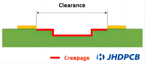
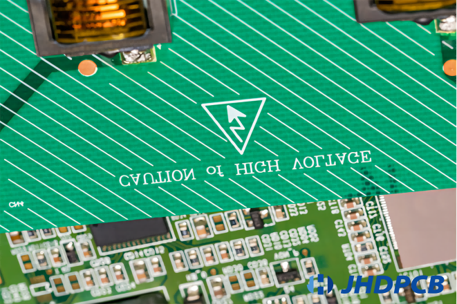
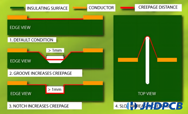
When designing printed circuit boards that conduct high voltages, it is important to consider the distances between metal conductors on the board to prevent electrostatic discharge and potential damage to the board and its components. This spacing is typically measured in two ways:

spacing is typically measured in two ways

  1. Creepage
    Creepage distance pertains to the spacing between two conductors on the PCB surface or along the insulating material’s surface. This measurement is important because even if two conductors are not directly touching each other, there may still be a risk of arcing if they are too close together. Creepage distance is particularly important for PCBs that are exposed to high levels of moisture or contamination, which can increase the risk of current leakage between conductors.
  2. Clearance
    On the contrary, clearance refers to the line-of-sight distance between two conductors through the air. In other words, clearance is the minimum air gap required between conductors to prevent arcing. Clearance distance is particularly important for high voltage circuits where the voltage exceeds 30VAC or 60VDC.
    In certain scenarios, the creepage and clearance distances may coincide, particularly when measuring the distance between two component pads or exposed metal areas on an unobstructed section of the board. However, in other cases, the two distances may be different depending on the placement of components or any unusual contours of the raw board.PCB designers must carefully consider both the difference between creepage and clearance distances and their individual requirements when designing high voltage circuits to ensure the safety and reliability of the board and its components.
    It is also recommended to follow industry standards and guidelines related to these measurements, such as those provided by the International Electrotechnical Commission (IEC) and Underwriters Laboratories (UL).

What about the type of circuit for PCB creepage and clearance?

The type of circuit for clearance and creepage in pcb depends on the specific requirements of the application and the standards/regulations, such as the creepage and clearance distance standards, that need to be followed.Here are a few common types of circuits and their associated creepage and clearance requirements:

Low Voltage Circuits: For circuits operating at low voltages (e.g., below 50V), relatively smaller creepage and clearance distances are typically sufficient. The precise distances can fluctuate based on factors such as pollution level, insulation coordination, and adherence to safety regulations.

the type of circuit for PCB creepage and clearance

  • High Voltage Circuits: Circuits operating at high voltages (e.g., above 50V) require larger creepage and clearance distances to ensure safe operation and prevent electrical breakdown. The specific creepage and clearance distances for high voltage circuits can vary depending on various factors, including the voltage level, pollution degree, material properties, and relevant standards.
  • Power Electronics Circuits: Power electronics circuits, which involve high currents and high voltages, often require larger creepage and clearance distances. This is to mitigate the risk of arcing and insulation failure due to the higher energy levels involved. The distances are determined based on the specific voltage and current ratings, as well as applicable safety standards and regulations.
  • Medical/Healthcare Circuits: PCBs used in medical or healthcare applications often have stricter creepage and clearance requirements due to the critical nature of the equipment. Standards such as IEC 60601-1 specify specific distances based on various factors like patient contact, applied parts, and working voltage.
  • Industrial Circuits: Industrial applications may have varying creepage and clearance requirements depending on the specific environment and safety regulations. These circuits may need to account for factors like high humidity, dust, vibration, and temperature variations.

In summary, the type of circuit for PCB creepage and clearance is determined by the voltage levels, current ratings, application requirements, and relevant safety standards/regulations. Thoroughly evaluating these factors is imperative in order to guarantee dependable and safe functioning of the PCB.

Design guidelines for PCB creepage and clearance issue.

Design guidelines for PCB creepage and clearance issue

Establishing design guidelines for PCB creepage and clearance is essential to uphold the circuit’s safe and dependable operation. Here are some key guidelines to consider:

  1. Understand the Requirements: Familiarize yourself with the specific requirements for creepage and clearance distances based on the application, voltage levels, current ratings, and applicable standards/regulations. Standards like IEC 60664 and IPC-2221 provide guidelines for determining these distances.
  2. Identify High Voltage Areas: Identify the areas of the PCB where high voltage components or traces will be present. These areas will require larger creepage and clearance distances to prevent arcing and electrical breakdown.
  3. Keep Traces and Components Isolated: Maintain sufficient spacing between high voltage traces and components to minimize the risk of creepage and clearance violations. Use wider spacing and consider using larger PCB layers to create adequate isolation.
  4. Consider PCB Layer Stackup: In multi-layer PCBs, consider the layer stackup to ensure proper creepage and clearance distances between different voltage layers. Utilize dedicated ground and power planes to segregate areas of high voltage and low voltage.
  5. Use Insulating Barriers: Implement physical barriers or insulation materials to create separation between high voltage and low voltage areas. These can include slots, slots with coverlays, or insulation coatings.
  6. Minimize Edge Clearance: To prevent arcing across the edges of the PCB, maintain a sufficient clearance distance between high voltage traces and the board edge. This is particularly important for high voltage circuits operating in humid or polluted environments.
  7. Consider Conformal Coating: Apply conformal coating over the PCB to enhance insulation and protect against moisture and contaminants. This approach can offer an extra level of safeguarding for meeting the creepage and clearance criteria.
  8. Consider Air Flow and Ventilation: Adequate air flow and ventilation can help reduce the risk of arcing and improve insulation performance. Ensure sufficient spacing and proper heat dissipation to prevent heat buildup and potential insulation failure.
  9. Verify with Testing: Perform thorough testing and inspection of the PCB to ensure compliance with the required creepage and clearance distances. Use high voltage testing equipment to verify insulation performance and identify any potential issues.
  10. Document and Follow Standards: Maintain detailed documentation of the design, including the chosen creepage and clearance distances, materials used, and any testing performed. Follow relevant standards and regulations to ensure compliance and safety.

By following these design guidelines, you can effectively address creepage and clearance issues and ensure the safe and reliable operation of your PCB.

The question of PCB Trace Spacing

PCB trace spacing is important for several reasons. Firstly, it ensures electrical safety by preventing arcing or short circuits between adjacent traces. Additionally, it aids in preserving signal integrity by reducing crosstalk and interference among traces. Lastly, it allows for proper heat dissipation and reduces the risk of thermal issues.

The determination of PCB trace spacing depends on several factors, including the operating voltage, environmental conditions, and applicable industry standards. Standards such as IPC-2221 provide guidelines for trace spacing based on voltage levels and desired level of electrical isolation. Designers also consider factors like trace width, board thickness, and the presence of insulation materials to calculate an appropriate trace spacing.

Inadequate trace spacing can lead to various problems. Insufficient spacing may result in electrical arcing between traces, leading to shorts or even board failures. It can also cause crosstalk, where signals from one trace interfere with adjacent traces, degrading signal quality. In high-power applications, inadequate spacing can cause excessive heat buildup, affecting component performance and reliability.

Ensuring proper trace spacing requires careful consideration during the design phase. Designers should consult relevant industry standards and guidelines to determine the required spacing for their specific application. Utilizing PCB design software with built-in design rule checks can help identify and flag potential spacing violations. Collaborating with experienced PCB manufacturers and seeking their expertise can also ensure compliance with trace spacing requirements.

Absolutely! JHDPCB has a team of experienced engineers who specialize in PCB design and manufacturing. We can provide design review and consultation services to ensure your PCB meets the necessary trace spacing requirements. Our expertise and state-of-the-art facilities enable us to manufacture PCBs with precise trace spacing, meeting the highest industry standards for electrical safety and performance.

Yes, there are industry standards that provide guidelines for PCB trace spacing. The IPC-2221 standard, for example, offers recommendations based on voltage levels and the required level of electrical isolation. This pcb trace spacing standard takes into account various factors such as pollution degree, working environment, and insulation coordination. Other standards, such as IEC 60664, also provide guidelines for determining appropriate trace spacing based on factors like working voltage, clearance requirements, and pollution degree.

Indeed, trace spacing requirements can differ based on the particular application at hand. High voltage and high power applications typically require larger trace spacing to ensure sufficient electrical insulation and prevent arcing. Low voltage and low-power applications may have more relaxed spacing requirements. Additionally, certain industries such as automotive, aerospace, and medical may have stricter trace spacing requirements due to the critical nature of the applications and the need for enhanced safety and reliability.

Yes, ensuring electrical safety involves more than just trace spacing. Other factors to consider in the design process include clearance distances, creepage distances, and the selection of suitable insulation materials. Clearance distance refers to the distance between a trace and any conductive material that is not part of the same electrical circuit.Creepage distance pertains to the minimum distance along the surface of a PCB between two conductive components.These distances are determined by factors like voltage levels, pollution degree, and applicable safety standards.

PCB design software often includes design rule checks (DRC) that can help identify spacing violations. These tools analyze the PCB layout and compare it against specified design rules, including trace spacing requirements. DRC can flag any violations, allowing designers to make necessary adjustments. Additionally, conducting thorough inspections and utilizing 3D visualization tools can help identify potential spacing issues and ensure compliance with trace spacing requirements.

Yes, trace spacing can impact manufacturability and cost. Smaller trace spacing may require more precise manufacturing processes and higher quality materials, which can increase production costs. It is important to balance design requirements with manufacturing capabilities to optimize both performance and cost. Collaborating with PCB manufacturers, like JHDPCB, who have expertise in optimizing designs for manufacturability, can help ensure that trace spacing requirements are met efficiently and cost-effectively.

 A creepage and clearance calculator typically requires inputs such as voltage level, pollution degree (degree of contamination in the environment), material properties, and relevant standards. Based on these inputs, the calculator uses established formulas and guidelines to calculate the minimum creepage and clearance distances required for the specific application.

In conclusion, PCB trace spacing is a critical aspect of PCB design that directly impacts the safety and reliability of the circuit. Adhering to proper trace spacing guidelines helps prevent issues like arcing, electrical breakdown, and insulation failure. By following the design guidelines mentioned above, designers can ensure adequate creepage and clearance distances for different voltage levels and applications.
At JHDPCB, we understand the importance of PCB trace spacing and offer professional services to assist our customers in achieving optimal design solutions. Our team of adept engineers is knowledgeable in terms of industry standards and regulations associated with creepage and clearance specifications.We provide comprehensive design reviews, consultation, and guidance to ensure that our customers’ PCBs meet the necessary safety standards and deliver reliable performance.
With our expertise, state-of-the-art facilities, and commitment to customer satisfaction, JHDPCB is equipped to provide our customers with high-quality PCB manufacturing and assembly services while addressing specific trace spacing requirements. We are dedicated to supporting our customers throughout the design and production process, ensuring their PCBs meet all necessary specifications for creepage and clearance.

Get a PCB Quote Now

Open high-quality PCB manufacturing services in JHDPCB

Leave a Comment