
Rigid Printed Circuit Boards (PCBs) are the most popular and commonly used, but you may also consider using flex PCBs once you become more familiar with them, as they are now more readily available due to more manufacturers providing this type. However, many customers continue to lack an understanding of the difference between rigid and flexible PCBs.
The two rigid and flexible PCBs are used to connect electronic components in a variety of consumption and non-consumption devices. As the names suggest, rigid PCBs are built on a rigid substrates layer that cannot be bend, while flexible PCBs (also the flex circuits), are built on flexible substrates that can bend, twist and fold. The non-conductive substrate of a rigid circuit board usually contains fiberglass (mostly FR1-FR4), which Enhance the strength and rigidity of the board. The rigid PCBs will provide great support for PCB components and excellent heat resistance. They serve a good purpose on large products like televisions and desk computers.
Flexible PCBs use flexible substrates like polyimide. The flexible base enables the flex circuit to tolerate vibration, dissipate heat and fold into many shapes. Due to their structural properties, flexible circuits are increasingly used in in small and cutting-edge electronics, such as smartphones and wearable technologies. In this blog, we will focus on the flexible circuit boards and give a introduce of the necessary knowledge of the flex circuit design guide, including flex PCBs’ materials to how to choose a best flex PCB manufacturer. Now learn more about the characteristics of flexible PCBs below.

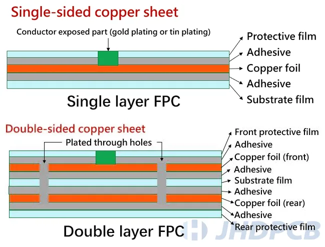
As happens for rigid PCBs, flexible PCBs (also called FPCs) can be classified as single-layer, double-layer, or multi-layer circuits. The basic structure of a single-layer flexible-printed circuit is as follows:
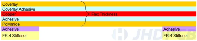
- Dielectric Substrate Films: Polyimide (PI), the main material of the flexible core and cover layers, is a dielectric flexible material with a uniform thickness and a dielectric constant (DK) value between 2.5 and 3.2 at 10GHz. Variations of DK will be eliminated by the absence of woven glass reinforcing. Thanks to its cast manufacturing process, polyimide features extremely uniform thickness, ranging from 0.5 to 4 mils. Polyimide (PI) films do not soften when heated and continue to be flexible after being heat-cured
- Electrical conductors: Generally made of copper, representing circuit traces, usually thin and ideal for both dynamic and static applications. Flexible circuits typically use 0.5oz (0.7 miles) of copper. The weights of 0.5oz and 1oz in flex PCB copper are the most popular. The optimum combination of the thinnest construction is made possible by the maximum copper weight of 2 oz.
- Flexible copper-clad laminate (FCCL): It is the core component of a flexible PCB and consists of multiple layers of copper foil and polyimide. Typically, these circuit boards use roll-annealed copper, which is produced by subjecting electrodeposited copper to a roll-annealing process. It provides a smaller bending radius. Copper’s ductility is improved as the vertical grain structure transforms into an elongated horizontal structure, making it appropriate for dynamic applications. Fully annealed or low-temperature annealed copper has better bending properties.
- Bondply: Bondply is composites materials comprised of polyimide sheets covered on both sides with B-staged acrylic adhesives. Bondply is utilized in between two conductive layers from distinct FCCL cores in heavy copper multi-layered constructions of flex/rigid-flex boards to encapsulate etched details.
- Protective finish: Coverlay, cover coat, photo-imaged dry film, and liquid photo-imaged polymer are used to protect the board surface. These various surface treatments can offer a solderable surface and stop copper oxidation.
- Adhesive material: Acrylic adhesives, epoxy adhesives, and pressure-sensitive adhesives (PSA) are just part of numerous types of adhesives that can be utilized in flex circuits. PSAs are incredibly adaptable, have exceptional bond strength, and are simple to use. They may directly stick to the substrate or other surfaces. Since epoxy cures hard, it is not suggested for use in dynamic operations.
- Stiffeners: By using localized rigid material known as PCB stiffeners, single-layer, double-layer, and multi-layer flex PCBs can be made more rigid where it is needed. This can increase the strength, thickness, and rigidity of mounting components by adding mechanical support. Materials like FR4 and Kapton are frequently employed as stiffeners and aluminum or stainless steel are occasionally utilized. Pressure-sensitive adhesives or acrylic thermally cured adhesives can be used to attach these materials. Strain reduction, weight balance, and heat dissipation are all possible uses for stiffeners, which can boost abrasion resistance and strengthen solder junctions.
It is crucial to comprehend two aspects of bendability: how frequently the board will flex and the extent to which it will flex. Whether the PCB is static or dynamic depends on how many times it can bend. A static board will flex less than 100 times in its lifespan and is regarded as bend-to-install. Mostly, it is bent while being assembled. The design of a dynamic board must be more durable because it bends frequently and must be able to resist thousands of bends.
The flex circuit’s flexibility is directly impacted by its thickness. The more pliability, the thinner the material must be. These boards’ thickness varies depending on a number of variables:
- Dielectric material selection;
- Copper layer count;
- Base copper weight;
- Adhesive thickness;
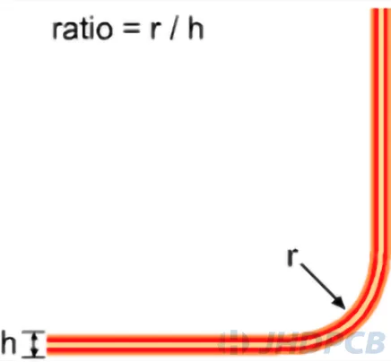
The bend radius is how much the bend area of the board can bend. The smallest angle at which the flexible area can bend must be determined early in the design process. By doing this, you may be sure that your design will permit the required number of bends without harming the copper. The bend radius is determined based on the number of layers in the circuit board. Bonded designs are necessary for bigger minimum bend radiuses when the flex circuit has three layers or more. The FPC is more flexible with the smaller the bending radius.
The bend ratio measures the relationship between the flex pcb thickness (T) and flex pcb bend radius (r). If the bend radius is smaller, the likelihood of failure is higher. The minimal bend ratio for several types of circuits according to IPC standard is listed below for a reliable flexible PCB design:
| Number of layers | Bend ratio for static boards | Bend ratio for Dynamic boards |
|---|---|---|
| Single-sided | 10:1 | 100:1 |
| Double-sided | 10:1 | 150:1 |
| Multilayer | 20:1 | Not recommended |
Note: Only single- and double-layer flexible printed circuit boards can reliably guarantee dynamic bending.
Layout for the bend areas of flexible pcb design:
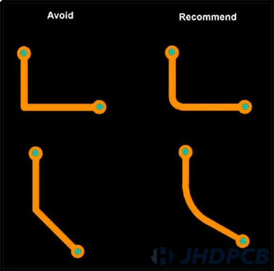
- Avoiding 90°bends as this results in high strain. Use gradual and large curved angles to avoid damaging circuits.
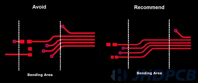
- Plating through-holes and component placement near bends should be avoided.
- Conductors traversing a bend area should be perpendicular to the bend axis.
- To increase the efficiency of a multi-layered circuit, stagger the conductors.
Put conductors with a diameter of fewer than 10 mils inside the neutral bend axis, which experiences the least compression or stress during flexing.
Although every PCB designer is familiar with routing traces, routing a flex design presents some special difficulties. When routing near bends areas, you must be careful. Vias and pins must not pass through the bend areas in order to protect the holes from damage. Traces must pass through such regions perpendicular to the bend line. Be cautious while stacking layers with traces running adjacent on top of one another. You should stagger the traces rather than doing this since it will add unwanted stiffness to the bend locations of the flex circuit. The layer architectures of flex circuits are distinct, and not all of the layers might be accessible in every area of the board. Designers must use caution when routing on layers that might abruptly drop out. Instead of using orthogonal routing, employ curved corners.
Consider the arrangement of preparatory components (SMT or TH) and decide if stiffeners are necessary for those components. A PCB’s circuitry architecture can make or destroy it. Key layout design and routing factors to take into account while designing flex PCBs include:
- Sharp angles reduce the longevity of a board, therefore a big bend radius is preferred.
- Curved traces result in lower stress than angled ones.
- Conductors ought to be run perpendicular to the overall bend. By doing this, the stress spots that can lead to trace copper breakage are removed.
- Traces on a flexible circuit board with two or more layers should be spaced apart.
- By avoiding l-beaming caused by stacked copper traces, the stress that could harm copper circuits is reduced.
- To stiffen the flex material at the inside bend radius and prevent tears, use tear guards in the circuit.
- Always taper down the traces from the thick to the thin as you gradually transition from wide to narrow traces.
- Keep the area around the bend free of discontinuities like vias, cut-outs, slits, and holes. When a via is bent, stress and cracks develop that ultimately lead to failures and malfunctions.
- Put an end cutouts slits in flex areas in accordance with IPC with circular sections(relief holes) to reduce tearing at corners. The radius ought to be larger than 0.75mm.
- Flex materials are more likely to move and compress during production. As a result, the drill to copper is an important aspect when constructing your flex board. Always leave at least 8 mils between the drill and the copper.
- Be aware of whether panel plating or pad-only plating (button plating) is best for your flex circuit. With button plating, copper is solely applied to the vias pads. Button plating offers greater versatility because it uses less copper. Manufacturers can better manage copper thickness and increase etch yields in intricate etch patterns. Due to conductor traces have a uniform copper thickness, width, and spacing, it also makes regulated impedance possible at faster speeds. The additional processing processes make it more expensive. Click to read detailed PCB trace spacing guidance.
On a flex circuit, a power or ground plane may occasionally be required. Utilizing solid copper pours is OK as long as you don’t mind the coppers dramatically decreased flexibility and potential buckling under tight-radius bends. In order to maintain a high amount of flexibility, it is typically advisable to employ hatched polygons.
Due to the placement of the hatch traces and “X” es, a typical hatched polygon still has significantly biased copper stresses in the 0°, 90°, and 45° angle directions. A hexagonal hatch layout would be more statistically ideal. Although a negative plane layer and a number of hexagonal anti-pads could be used to accomplish this, the hatch illustrated below can be easily built by cutting and pasting sections.

The tension biases can be distributed uniformly among the three angles by using hexagonally hatched polygons.
Consider the type of application (static dynamic), bend radius, number of layers, and overall board thickness when optimizing your flex PCB stackup. When creating the build-ups, keep the following principles in mind:
- Create flex board models as early in the design process as possible using rigid paper or mylar. With CAD technologies, virtual mock-up models can be created. The fundamental components can then be added, followed by gluing the rigid pieces to this using cardboard.
- Consider your material choices in light of the design and operating circumstances.
- Use flexible layers in the center of a rigid-flex board when constructing it to prevent sliding.
- Always aim to employ an even number of layers to obtain a balanced stack-up.
- Throughout your build-up, make sure to specify each layer’s thickness and impedance requirements.
- Select ECAD/MCAD tools that are industry-standard and provide a full toolkit for designing, outlining, and customizing stack-up in flex/rigid-flex board.
- Use the air-gap construction technique to rigid-flex structures to avoid using flex adhesives inside the stiff parts, hence addressing the reliability issues of vias.
Layer counts on flexible circuits can range from 1-6. If you need more layers of flexible PCB, please contact us for details. Due to their thickness, designs with more than three layers will have a restricted ability to flex. Consider the type of application (static dynamic), bending radius, layers, and thickness of board when optimizing your flex PCB stackup. Below are a few illustrations of typical material stack-ups used in the manufacture of flexible circuit boards.
Single-Layer Flexible Circuit:
- Applications(s): Connector to connector flex, functional circuit board.
- Depending on the completed thickness necessary to meet bend requirements, flexible core can either be adhesive-less or adhesive.
Double-Layer Flex Circuit:
- Common application(s): Surface microstrip controlled impedance, ZIF to ZIF interconnect, PTH or SMT Connector interconnect.
- Depending on the finished thickness necessary to meet bend requirements, flex core can be either adhesive-less or adhesive-based.
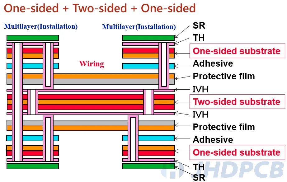
Multilayer Flex Circuit:
- Common application(s): Stripline controlled impedance, radio frequency (RF)/electromagnetic interference (EMI) shielded.
- FR4 or polyimide stiffeners are available.
- Flex cores are usually adhesive-less to reduce flex thickness and allow for bend needs.
- Higher layer counts available. It is advised to review the bend requirements.
Employing IPC standards for certain flex materials, performance, and assembly of flex PCBs while designing your flex circuit.
Pads are part of a conductor that are utilized to connect a component for an electrical connection and are often found surrounding a through-hole. The terms “terminals” or “lands” can also be used to describe pads. Due to the flexible nature of the circuit, all of the pads on a flex circuit are vulnerable to rising off the substrate and ought to be anchored. The copper pads’ ability to remain adherent to the base material may be compromised by stress from bending or flexing. Thus, it is crucial to offer support for exposed pads:
- If the circumstances allow, JHD will first advise adding 1.5 mils of through-hole plating to rigid-flex and flex circuits. This plating can give Z-axis support surface lands, while non-plated lands are referred to as unsupported.
- Especially for single-sided designs without a plated through-hole to help attach the pad, it is a good idea to make pad sizes larger to aid in stress relief. Generally speaking, flexible circuit boards have worse copper adhesion than boards made of FR4 material.
- To provide a more lasting connection, design pads to be larger than access holes whenever possible.
- Use hold-down tabs if available space is limited. In both flexible circuit assembly and rework, hold-down tabs, also the hold-down copper pads, which are extensions of the copper pad, are utilized to maintain the pad in place during soldering processes.
Vias may occasionally be required for multi-layer flex zones to migrate between layers. Vias should ideally not be positioned because they might quickly suffer fatigue during flexing motion. The potential problems that could result from the usage of vias, such as cracking, breaking, or peeling in the flexible material, must be taken into consideration during flex circuit design. Vias have a higher risk of coming away from the flex layers. You can put the following strategies into practice to make vias on flexible circuit boards more stable:
- To connect traces or plated through-holes on flex boards, use teardrop (pad fillets) shaped vias. This lessens the likelihood of stress concentration spots. When the pad diameter is more than the connecting strand’s breadth, fillets connections are appropriate.
- Give annular rings the biggest possible size. They are mostly used to create a strong connection between a via and a copper trace. For flex PCB, the annular ring should be at least 8 mils.
- Also, adding tabs or anchors to vias will assist stop peeling.

- Vias should not be placed in bends. Use “rooms” to identify locations where you know there won’t be any bends (if you must have vias in a flex circuit), and then utilize the PCB editor’s design rules to limit via a placement to those fixed regions.
- Vias that are placed over a stiffener are safe, but those that are placed just off its edge are susceptible to cracking.
- At least 20 mils should separate the rigid-flex/flex interface from the placement of vias.