Chip Scale Package: A Guide to CSP Package Forms and Types

jhdpcb@gmail.com
What is CSP chip scale package?
Based on the CSP chip scale package definition of IPC/JEDEC J-STD-012, CSP (Chip Size Package) is a single-chip, a type of surface-mountable integrated circuit package whose package substrate size does not exceed 120% of the semiconductor chip size. Originally, the acronym “CSP” used to stand for “Chip Scale Package,” but since only a few packages are chip-sized, the acronym’s meaning was adapted to Chip Scale Package CSP. The most important goal of CSP BGA package is to reduce the size of the mounting area and reduce area.
The definition of a CSP says nothing about how it needs to be manufactured or constructed. Any package that meets the defined dimensional requirements and has surface mount capability can be considered a CSP. When classified as a chip-scale package, the structural size is not considered too much. As a result, the industry has developed a variety of chip-scale packages, and no general assumptions can be made about the manufacturability or reliability of CSPs as a homogeneous package group. There are more than 50 different classes of chip-scale packages in the CSP electronics industry, and they are still growing.
At the beginning of a typical CSP process, chips are mounted on an interposer using epoxy. The epoxy is usually a non-conductive type, but conductive epoxy is also used when the backside of the die needs to be connected to a circuit. The die is then wire bonded to the interposer using gold or aluminum wires. These wire bond profiles are as low as possible and as close to the die as possible to minimize package size. This is followed by plastic encapsulation, usually by transfer molding, to protect the chips and wires. After packaging, solder balls are attached to the bottom of the interposer. Finally, the package is marked and the part is separated from the leadframe.
Features of Chip Scale Packaging.
- Chip-scale packaging has many advantages of chip scale packaging csp technology. One of their biggest advantages over traditional packages is the reduced package size. The BGA design of the package increases the number of interconnects, so there is a reduction in size. It has the advantages of smaller size (smaller footprint and thickness), lighter weight, relatively easier assembly process, lower overall production cost, and improved electrical performance.
- Self-alignment characteristics and no bent leads are another advantage of chip-scale packaging, which can further help reduce manufacturing costs. Unlike other packages, chip-scale packaging can utilize existing surface mountable technology (SMT) and is easier to start manufacturing. They are also tolerant to die size variations, as the interposer design can still accommodate the shrinking die size without changing the CSP footprint.
- Add to this the size and performance advantages of bare die assembly and the reliability of encapsulated devices. They are usually built using lead frames, allowing mass assembly of many packages. This maximizes the use of interposer area and allows many devices to be fabricated using the same substrate.
- Other key features include:
Flexible tools for custom packages;
Single-chip designs are typically 20% larger than die size;
5mm pitch to 1.27mm pitch;
Capable of package height <1mm;
Competent at MSL Level 3.
What are the common forms of CSP?
Common forms of CSP Several forms include: flip chip, non-flip chip, wire bonding, ball grid array, and leaded. These five forms will be introduced one by one next.
- Flip-chip CSP (FCCSP)
- Non-flip-chip
- Wire-bonded
- Ball Grid Array
- Leaded
Flip-chip CSP (FCCSP):
Flip-chip refers to turning the chip upside down and attaching it to the substrate or lead frame. Compared with general CSP, the difference is that it uses bumps such as solder or copper pillars for interconnection instead of traditional wire bonding. I/O pads can be distributed over the entire surface of the chip, allowing chip size to be reduced through optimized circuit paths. The absence of bond wires also helps reduce signal inductance. FCCSP (Flip Chip CSP Package) provides chip scale capacity for approximately 200 I/Os or less. FCCSP offers better chip protection and better solder joint reliability than Direct Attachment (DCA) or Attachment-on-Board (COB). FCCSP features a low-profile, small-profile, and lightweight package. FCCSP is over molded in two ways: one using capillary underfill (CUF) and the other using epoxy molding compound instead of underfill (MUF) to reduce cost, improve thermal performance and secondary reliability .
Non-flip-chip:
Non-flip chip, also known as front mount chip, is the earliest chip structure. From top to bottom, the structure is: electrode, P-type semiconductor layer, light emitting layer, N-type semiconductor layer and substrate. In this structure, the heat generated by the PN junction needs to be conducted to the heat sink through the sapphire substrate. The poor thermal conductivity of the sapphire substrate leads to poor thermal conductivity of the structure, thereby reducing the luminous efficiency and reliability of the chip. In the positive chip structure, both the p-electrode and the n-electrode are located on the light-emitting surface of the chip, and the shielding of the electrodes will affect the luminous efficiency of the chip, resulting in a low luminous efficiency of the chip; the positive and negative electrodes are located on the same side of the chip, which is prone to current congestion and reduces Luminous efficiency; In addition, factors such as temperature and humidity may also cause electrode metal migration. As the chip size shrinks and the spacing between positive and negative electrodes decreases, electrode migration may cause short circuit problems.
Wire-bonded:
Wire bonding is the process of creating electrical interconnections between semiconductors (or other integrated circuits) and silicon chips using bonding wires, which are thin wires made of materials such as gold and aluminum. Although less common, wire bonding is used to connect ICs to other electronic devices or to connect one printed circuit board (PCB) to another. Wire bonding is generally considered the most cost-effective and flexible interconnection technique used to assemble the vast majority of semiconductor packages. Wire bonding can be used for frequencies above 100 GHz. The two most common processes are gold ball bonding and aluminum wedge bonding.
Ball Grid Array:
A Ball Grid Array (BGA) is a surface mount package (chip carrier) for integrated circuits. BGA packages are used to permanently mount devices such as microprocessors. BGAs can provide more interconnect pins than dual in-line or flat packs. The entire underside of the device can be used, not just the perimeter. The traces connecting the package’s leads to the wires or the die to the package’s balls are also shorter on average than perimeter-only types, enabling better performance at high speeds.
Leaded:
Chip-On-Lead (COL) is a technology that mounts a die or crystal on the leads of a lead frame instead of pads. To complicate matters further, unlike conventional leadframes, this leadframe has no tape for support during wire bonding.
What are the types of CSP chip scale package?
Chip scale packages can be classified into the following groups:
- Customized leadframe-based CSP (LFCSP)
- Flexible substrate-based CSP
- Flip-chip CSP (FCCSP)
- Rigid substrate-based CSP
- Wafer-level redistribution CSP (WL-CSP)
Customized lead frame-based CSP (LFCSP)
LFCSP is a near-chip scale package (CSP), a plastic encapsulated wire bond package in a leadless package format with a copper lead frame substrate. Perimeter I/O pads are located on the outer edge of the package. Electrical contact to the printed circuit board (PCB) is made by soldering the perimeter and exposed pads on the bottom surface of the package to the PCB. Heat can be effectively conducted away from the package by soldering the exposed thermal pad to the PCB. Provides a stable electrical ground connection through bond down and through conductive chip attach material. Wire bonding is provided using gold wire. The perimeter and thermal pad surface finish is Sn/Pb solder or 100% Sn. Packaged in tape and reel or tray.
Flexible substrate-based CSP
The short definition of a flexible circuit is “a patterned arrangement of printed wiring utilizing a flexible substrate, with or without a flexible cover.” Flexible circuits are most commonly fabricated using one of two substrates, polyimide or polyester. Polyimide is favored where soldered components are required, while polyester is typically used in low-cost applications. Polyimide is also the material of choice for nearly all CSPs and flexible BGAs; however, polyester has been successfully used to make smart cards, arguably a large chip package that deserves some visibility. Flex circuits are produced in several basic forms, often parallel to rigid PWB structures. Products usually come with an overlay. The cover layer is typically a polymeric film of the same family as the base film with an integral adhesive layer. However, other processes and materials can also be used. Click to see more PCB types supported by JHD.
Flip-chip CSP (FCCSP)
Flip-chip refers to turning the chip upside down and attaching it to the substrate or lead frame. Compared with general CSP, the difference is that it uses bumps such as solder or copper pillars for interconnection instead of traditional wire bonding. I/O pads can be distributed over the entire surface of the chip, allowing chip size to be reduced through optimized circuit paths. The absence of bond wires also helps reduce signal inductance. FCCSP (Flip Chip Chip Scale Package) provides chip scale capacity for approximately 200 I/Os or less. FCCSP offers better chip protection and better solder joint reliability than Direct Attachment (DCA) or Attachment-on-Board (COB). FCCSP features a low-profile, small-profile, and lightweight package. FCCSP is over molded in two ways: one using capillary underfill (CUF) and the other using epoxy molding compound instead of underfill (MUF) to reduce cost, improve thermal performance and secondary reliability.
Laminate-substrate-based CSP
Laminate-substrate-based CSPs are an extension of National Semiconductor’s current Plastic Ball Grid Array (PBGA) technology and are the package of choice for portable applications. CSPs are available in two package designs: laminated CSPs and fine-pitch ball grid arrays (FBGAs). FBGAs are interconnected to the board using solder ball technology, while laminated CSPs use peripheral nickel-gold pads to interconnect the package to the board. The structures and materials used in these packages are designed to provide National Semiconductor’s new micro Products provide the highest performance and reliability. Laminate CSPs are available in Plastic Thin-Profile Fine-Pitch Quad Flat No-Lead Package (P-TFQFN) and Plastic Thin-Profile Shrink Small Outline No-Lead Package (P-TSSON) packages.
Wafer-level redistribution CSP (WL-CSP)
CSPs can be mass-produced by semiconductor manufacturers at the wafer level csp package, reducing costs and increasing yields. In their production, through several steps, the I/O pads are redistributed to facilitate bump formation. The bumped dies are then packaged and singulated. To redistribute the pads and form the bumps, a photolithography process similar to that used when the IC was originally manufactured is used.
| CSP Chip Scale Package Type | |||||
|---|---|---|---|---|---|
| Packaging Type | Construction | Advantages | Examples | Types | Applications |
| Leadframe-Based CSP | Copper leadframe, low-loop wire bonds or flip-chip interconnect, over-molded | 50% size reduction compared to thin-shrink small-outline package (TSSOP) inductance (MicroLeadFrame®) and very low inductance flip-chip MicroLeadFrame | MicroLeadFrame® (wire bond) and flip-chip MicroLeadFrame® (fcMLF) (Amkor) | Quad flat pack no lead (QFN), small outline no lead (SON), Dual flat pack no lead (DFN) | Portable electronics (cell phones and personal data assistants) (PDAs), MicroLeadFrame®and high-performance applications in the 5–40 GHz range |
| Exposed die-attach pad | 50% reduction in inductance/capacitance compared to leaded parts | MLP (MicroLeadFrame Package) (Carsem) | QFN, SON, MLPQ (quad format), and MLPD (Dual format) | PDAs, Global-Positioning Systems (GPS), RF product for Bluetooth™ | |
| Flexible Interposer CSP | Polyimide flex substrate (single electrical layer), wire bonded and overmolded | Significant area reduction compared to quad flat packs Cost parity with QFPs | MicroStar™ BGA (Texas Instruments) | MicroStar™ and MicroStar™Junior BGA | Consumer-based end equipment using digital signal processor solutions (wireless communication, laptop computers, and hard-disk drives) |
| Wire Bonding Silicon Die to Polyimide Tape | Not applicable | Flex Tape Chip Scale BGA | CS144/CSG144 | Not applicable | |
| Bumped Chip Carrier (BCC) and BCC+ based CSP | Standard bumped chip carrier and electrically/thermally enhanced center-exposed-pad technology, over-molded. | 40% less mounting area an 67% less mounting volume compared to Shrink Small Outline Package | BCC, BCC+ (Fujitsu) | Single-chip and stacked chip scale package | RF devices, wide area networks, and Dense Wavelength Division Multiplexing systems |
| Rigid laminate substrate (with or without soldermask), wire bonds, over-molded | Small outline, low profile (1.0 mm), enhanced electrical performance over 2.4 GHz, JEDEC moisture sensitivity level (MSL) 3 | Land grid array and fine-pitch ball-grid array (National) | Thin, fine-pitch QFN, Thin shrink SON | Portable applications, including cellular phone, wireless, lap-top computers, and DSP | |
| FR-5 laminate substrate | Improved signal-to-noise ratio (> 1 GHz) compared to wire-bonded parts and low-inductance die interconnects | ChipArray® Ball Grid Array (Amkor) | fcCSP | Cell phones, handheld electronics, and high-performance workstations (notebooks and RF applications) | |
| Laminate-Substrate-Based CSP | Rigid laminate substrate (with or without soldermask), wire bonds, over-molded | Small outline, low profile (1.0 mm), enhanced electrical performance over 2.4 GHz, JEDEC moisture sensitivity level (MSL) 3 | Land grid array and fine-pitch ball-grid array (National) | Thin, fine-pitch QFN, Thin shrink SON | Portable applications, including cellular phone, wireless, lap-top computers, and DSP |
| FR-5 laminate substrate | Improved signal-to-noise ratio (> 1 GHz) compared to wire-bonded parts and low-inductance die interconnects | ChipArray® Ball Grid Array (Amkor) | fcCSP | Cell phones, handheld electronics, and high-performance workstations (notebooks and RF applications) | |
| Wafer-level CSP (WLCSP) | Repassivation and deposition of solder bumps | Eliminates need for underfill, standard SMT process, minimal footprint per I/O, saves space on PWB | WLCSP (country) | micro patch | Not applicable |
| Polyimide layer for redistribution traces, overmolded | 30% smaller board area and 65% thinner profile | Super CSP (Fujitsu) | ball grid array, planar grid array | Flash and ASICs | |
What different of csp package and cob package?
- Chip Scale Package (CSP)
CSP recommends that the sensor chip bundle be no more than 1.2 times the area of the chip itself. This is done by the sensor manufacturer, usually with a layer of glass covering the chip. - Chip on Board (COB)
COB means that the sensing unit chip will be bonded directly to the PCB (Printed Circuit Card) or FPC (Flexible Printed Circuit). The COB process is part of the camera module manufacturing process, so it is completed by the camera component supplier.
Difference Between The Two.
The biggest difference between CSP PBC and COB is that the photosensitive surface of the CSP packaged chip is protected by a layer of glass, and COB is not equivalent to a bare chip. For the same lens, the module heights of the two processes are different, and the COB should be low. During the production and processing of CSP, the dust point is required to be relatively low. If there are still dust spots on the sensor surface it can be reprocessed, COB cannot.
Comparing the two product packaging options, the CSP process is faster, more accurate, more costly, and may suffer from poor optical path, while the COB is more space efficient and more affordable, but the process time is longer, the payoff is more troublesome, and it cannot be repaired.
CSP package VS BGA package.
For novices who have just taken BGA rework, many people don’t know how to distinguish BGA packages from CSP packages. Today I will explain the difference between these two packaging methods.
First let’s look at the difference between the concept of BGA package and CSP package. Their solder ball forms are divided into partially distributed and fully distributed.
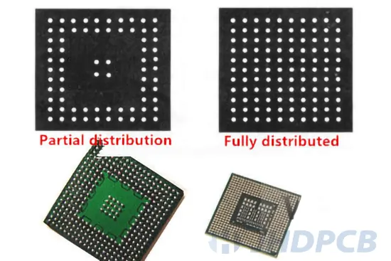
BGA ball grid array package.
With the development of integrated circuit technology, packaging requirements for integrated circuits have become more stringent. This is because the csp package technology is related to the functionality of the product. When the frequency of the IC exceeds 100MHz, the traditional packaging method may produce the so-called “CrossTalk” phenomenon. When the IC pin number is greater than 208 Pins, the traditional packaging method Its difficulty. Therefore, in addition to the QFP packaging method, most high-pin count chips (such as graphics chips and chip sets) are now using BGA (Ball Grid Array Package) package technologies. BGA has become the best choice for high-density, high-performance, multi-pin packages such as CPUs and south / north bridge chips on motherboards.
BGA packaging technology can be divided into five categories:
- PBGA (Plasric BGA) substrate: generally a multilayer board composed of 2-4 layers of organic materials. Among Intel series CPUs, Pentium II, III, and IV processors use this package.
- CBGA (CeramicBGA) substrate: ceramic substrate, the electrical connection between the chip and the substrate is usually mounted by Flip Chip (FC). Among Intel series CPUs, Pentium I, II, and Pentium Pro processors have all used this package.
- FCBGA (FilpChip BGA) substrate: a rigid multilayer substrate.
- TBGA (TapeBGA) substrate: The substrate is a strip-shaped soft 1-2 layer PCB circuit board.
- CDPBGA (Carity Down PBGA) substrate: refers to the chip area (also known as the cavity area) with a square low depression in the center of the package.
The BGA package has the following characteristics:
- Although the number of I / O pins increases, the distance between the pins is much larger than the QFP packaging method, which improves the yield.
- Although the power consumption of the BGA is increased, since the controllable chip chip welding is used, the electrothermal performance can be improved.
- The signal transmission delay is small, and the adaptive frequency is greatly improved.
- Co-planar welding can be used for assembly, which greatly improves reliability.
After more than ten years of development, the BGA packaging method has entered the practical stage. In 1987, Japan’s Citizen Corporation began to develop a chip (ie, BGA) packaged with a plastic ball grid array. Later, Motorola, Compaq and other companies also joined the ranks of developing BGA. In 1993, Motorola pioneered the application of BGA to mobile phones. In the same year, Compaq applied it to workstations and PCs. Until five or six years ago, Intel started using BGA in computer CPUs (ie Pentium II, Pentium III, Pentium IV, etc.) and chipsets (such as i850), which played a role in boosting the expansion of BGA application fields. At present, BGA has become an extremely popular IC packaging technology. Its global market size was 1.2 billion pieces in 2000. More detailed BGA assembly knowledge can be learned through our corresponding blog.
CSP chip size package.
With the global demand for personalized and lightweight electronic products, packaging technology has advanced to CSP (Chip Size Package). It reduces the size of the package size of the chip, so that the size of the bare chip can be as large as the package size. That is, the size of the packaged IC is no more than 1.2 times the side length of the chip, and the IC area is only no more than 1.4 times larger than the die.
CSP Chip Scale size packaging Type:
- Lead Frame Type (representative manufacturers) include Fujitsu, Hitachi, Rohm, Goldstar and so on.
- Rigid Interposer Type (Rigid Interposer Type), representing manufacturers such as Motorola, Sony, Toshiba, Panasonic and so on.
- Flexible Interposer Type (soft interposer type), the most famous of which is Tessera’s microBGA, CTS’s sim-BGA also uses the same principle. Other representative manufacturers include General Electric (GE) and NEC.
- Wafer Level chip scalePackage (Wafer Size Package): Different from the traditional single-chip packaging method, WLCSP is to cut the entire wafer into individual chips. Manufacturers investing in R & D include FCT, Aptos, Casio, EPIC, Fujitsu , Mitsubishi Electronics, etc.
The CSP package has the following characteristics:
- CSP is only smaller in size, smaller than CSP is called FC (Flip Chip).
- Flip Chip is called flip chip in our SMT assembly, which is to solder the bare chip directly to the PCB.
- BGA is very wide, CSP is just one of them.
- Just a small package.
- Generally less than 1: 1.2.
- Different pitches.
- BGA pitch (1.0mm1.27mm)
- CSP pitch <0.8 mm
In summary, BGA package and CSP package have their own different advantages and disadvantages. It is recommended that no matter what type of packaging method you choose, you need to consider the issue of post-maintenance.
Application field of CSP chip scale package.
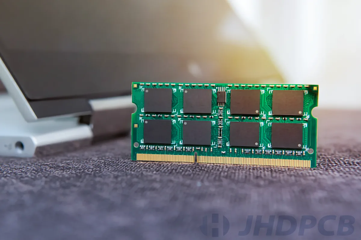
CSPs has significant size and weight. The size and weight reduction make them ideal for use in mobile devices such as cell phones, laptops, PDAs and digital cameras.
I believe that through the above packaging introduction, you have a general understanding of CSP chip-scale packaging. We have made a detailed description of the advantages and disadvantages of CSP, common forms, chip and package types, chip scale package csp led market etc. JHD has the best CSP packaging technology, if you need more information about CSP packaging or have any questions, please feel free to contact us. JHD’s professional customer service team will provide the best advice for your PCB production and assembly.