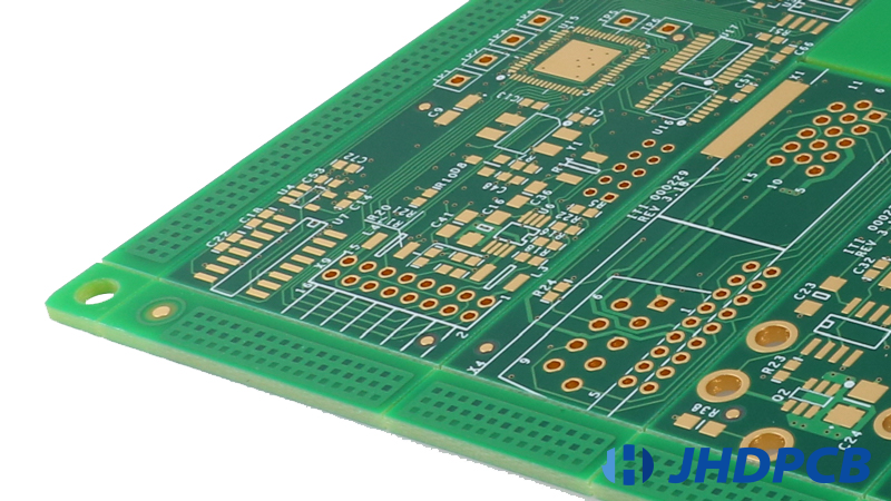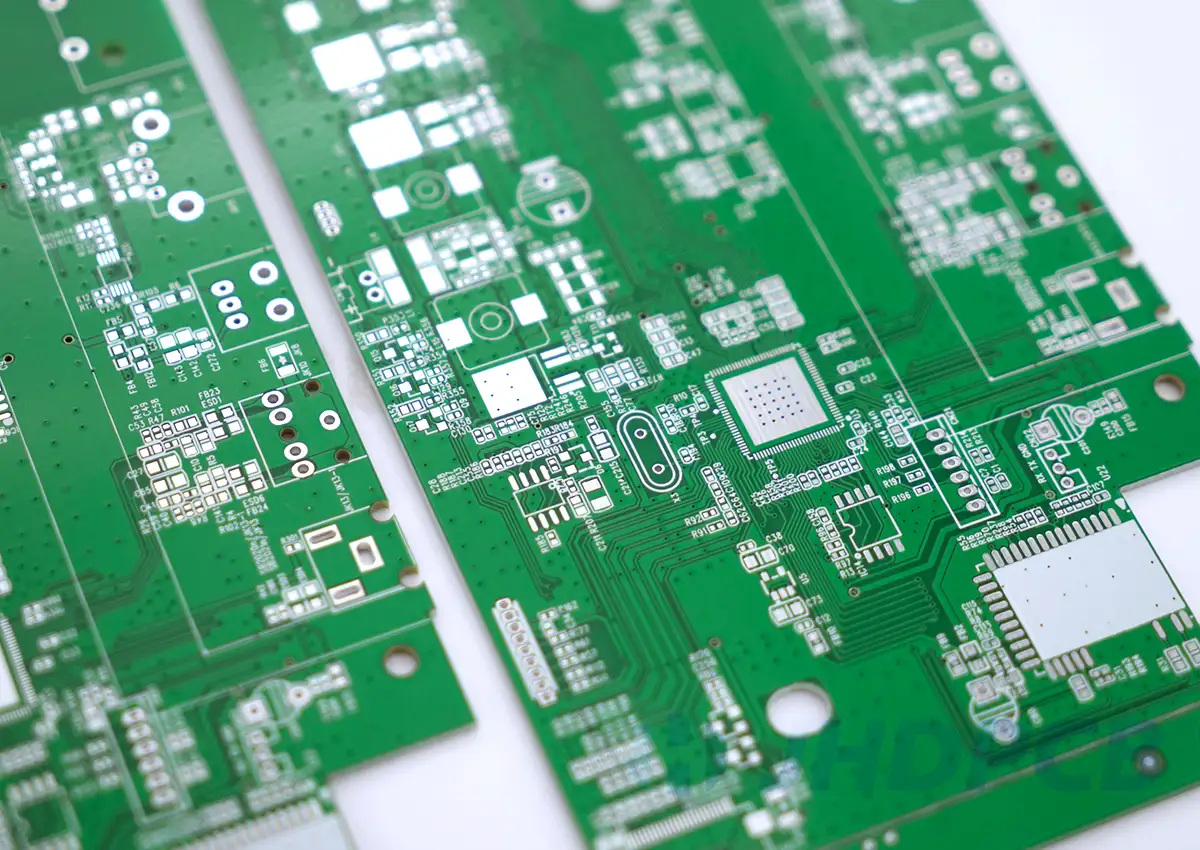

PCB solder pads are designed in various shapes to suit different application fields. In the following, JHDPCB lists some of our commonly used shape layouts. Regardless of the desired shape, including single-sided, double-sided contact pads, and a variety of customized pads. JHDPCB production and customer service teams are happy to provide you with high-quality services.
Metal domes are usually placed on a gold or tin contact plate, and each JHD metal dome has a corresponding PCB contact pad. Below are the single-sided and double-sided contact pads, broken down by metal dome series. If you need design help or have any other questions, please feel free to contact us directly.
| Contact pads by dome series | |||
|---|---|---|---|
| Series name | Legend display | Series name | Legend display |
| F-SERIES |
| GX-SERIES |
|
| S-SERIES |
| SQ-SERIES |
|
| M-SERIES |
| RCG-SERIES |
|
| WT-SERIES |
| BL-SERIES |
|
| RK-SERIES |
| P-SERIES |
|
| U-SERIES |
| E-SERIES |
|
| DT-SERIES |
| TC-SERIES |
|
| FB-SERIES |
| TB-SERIES |
|
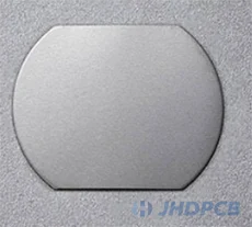
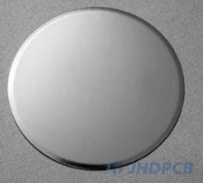
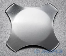
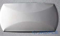
| Special-shaped customized pad series | ||
|---|---|---|
| Shape type | Introduction | Example diagram |
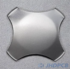
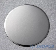
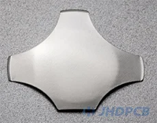
| Single sided | (Suitable for F, U, TC, SQ, GX, and RCG Series domes) The single-sided PCB pad is ideal for four-sided domes and also does not affect the track when the dome is activated. | 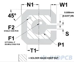 |
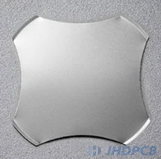
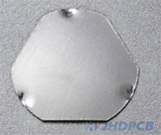
| Double sided | (Suitable for all domes except oblong) Double sided PCB pads are available for all dome styles except elongated and dual action (DT-Series) | 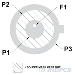 |
| Solder dome | Solder dome is suitable for the single-sided PCB pads ,also known as the S-Series. | 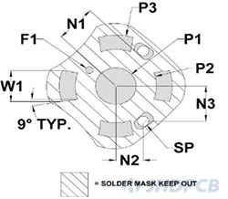 |
| Single sided 3-leg | (Suitable for WT-and E-TDF Series) 0.38mmSingle sided PCB pads can usually be used with three-leg domes, which included the WT-Series and E-TDF-Series. | 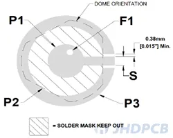 |
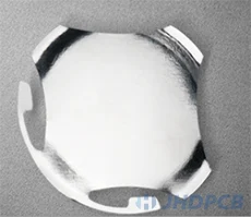
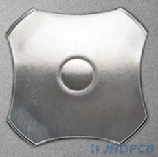
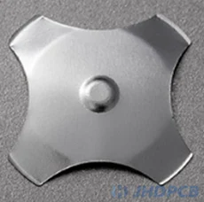
| Single sided with center led | (Suitable for BL-Series Domes) Single- sided PCB pads can be used with BL-Series domes with center hole for led. | 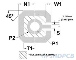 |
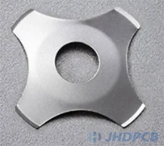
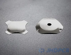
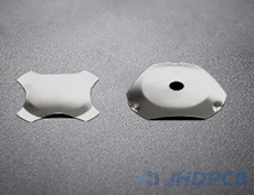
| Double sided with center led | Double sided PCB pads can also be used with BL-series domes with center for led. | 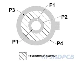 |
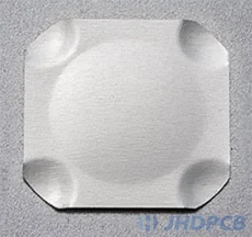
| Double sided oblong | (Suitable for RK-Series and E-Series oblong (ONN) domes) | 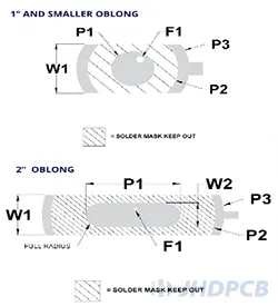 |
| Single& double sided (DT-Series) | (Suitable for DT-Series domes) Single-sided double action contact pads was pads with specifically designed to use with the DT-Series dual action domes. | 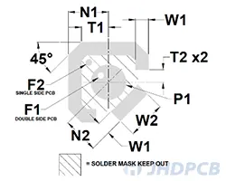 |
| Single& double sided contact pad 4-leg battery | (Suitable for FB-Series domes) Single and double sided contact pad was particularly used to use with the FE-Series battery contacts | 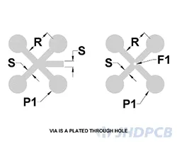 |
| Single& double sided contact pad 3-leg battery | (Suitable for TB-Series domes) Single and double sided pad contact pad was particularly designed to use with the TB-Series battery contacts. | 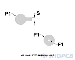 |
The pad stack is represented by a combination of letters and numbers representing different rubber sheet shapes and soil sizes. These combinations are used in conjunction with the terrain drawing conventions defined in the IPC-2220 design standard.
The first section of the pad stack notation contains the landforms written in lowercase. The six basic designations of the landforms are as follows:
- b-oblong;
- c-circular;
- d – D-shaped (square at one end and round at the other);
- r – rectangular;
- s – square;
- u – contour (refers to irregular shapes).
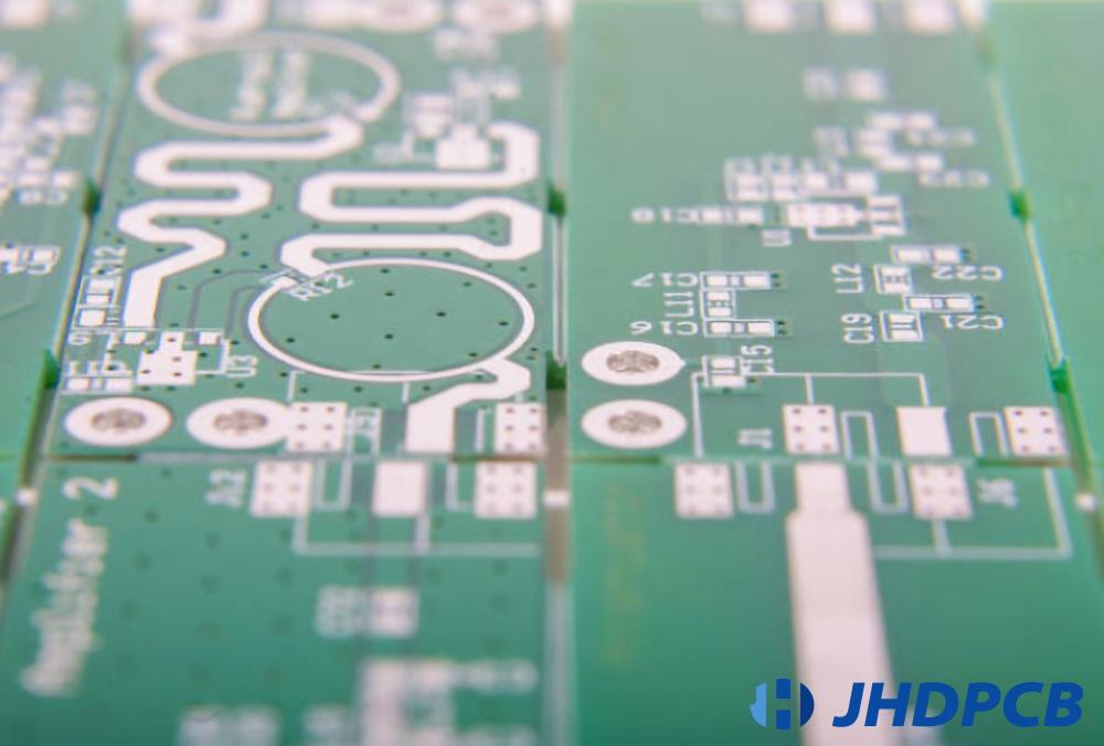
Finally, JHD not only works with conventionally shaped panels such as those mentioned above but can also produce custom-shaped panels to meet design and application requirements.
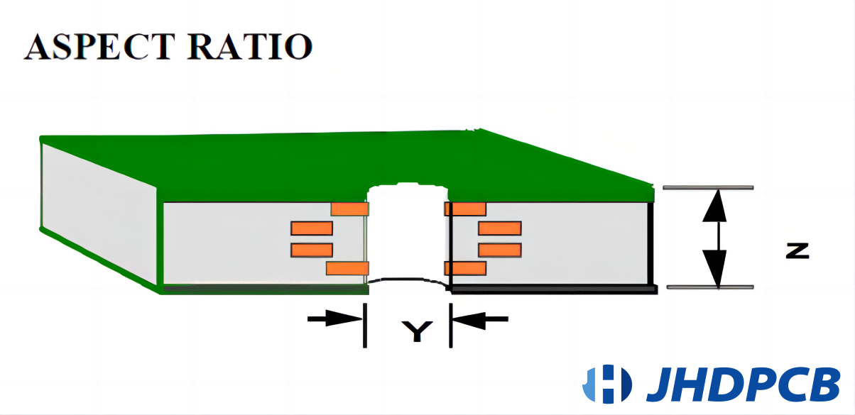
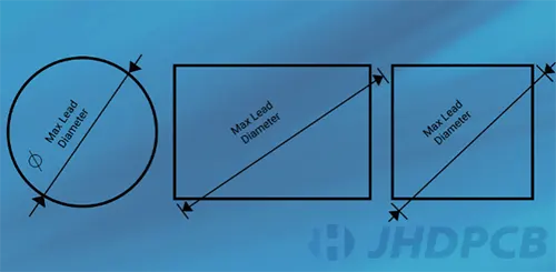
1. Determine the maximum diameter of the lead.
The maximum available conductor diameter shall be determined from the component enclosure drawing or data sheet. The following figure shows the maximum lead diameters for different geometries.
– Round PTH conductors require round holes.
– Rectangular PTH conductors require rectangular holes.
– Rectangular PTH conductors require rectangular holes.
2. Calculating the minimum diameter of the hole size.
The minimum bore diameter is calculated using the following formula
For IPC-2222 Level A: Minimum bore diameter = maximum conductor diameter + 0,25 mm (10mils).
For IPC-2222 Level B: Minimum bore diameter = maximum conductor diameter + 0.20mm (8mils).
For IPC-2222 Level C: Minimum inside diameter = maximum conductor diameter + 0,15 mm (6mils).
3. Calculation of pad diameter.
Once the minimum bore diameter has been calculated, the minimum loop size is 0.05 mm (50 mils); IPC-2221 states that for Level A the minimum tolerance is 0.6 mm, for Level B it is 0.5 mm and for Level C it is 0.4 mm.
Pillow diameter = minimum bore size + minimum ring size x 2 + manufacturing tolerance.
For level A IPC-2221: Cushion diameter = minimum bore size + 0.1 mm + 0.60 mm (24mils).
For IPC-2221 level B: Pillow diameter = minimum bore size + 0.1 mm + 0.50 mm (20mils).
For IPC-2221 level C: Cushion diameter = minimum bore diameter + 0.1 mm + 0.40 mm (16mils).
Check out the more detailed IPC-2221 standard in PCB Design.