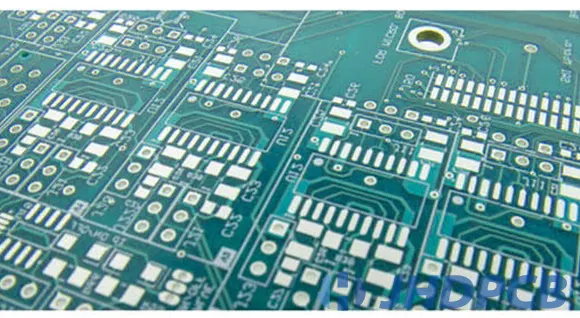
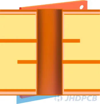
PCB via hole plating has plenty of other names, such as PCB hole plating, PCB through hole plating(PTH), and PCB plating through holes. Through-hole technology, by means of inserting their leads through the corresponding holes to enable the components installed on the PCB boards. These holes are referred to as through holes, which were drilled from the top to the base of boards. The PCB hole plating process refers to that drilled holes being filled with copper in order to offer a current path within the whole inner hole. The current path can extend from one board surface to another or from the surface of the board to the inner layer of the board, and between two inner layers. Such a conductive mode can benefit in the electrical connection between copper tracks and components. In addition to this, it can also decrease the entire resistance to offer a stationary current flow and boost mechanical stability. For copper plating PCB vias, the PCB via plating thickness is at least 20µm.
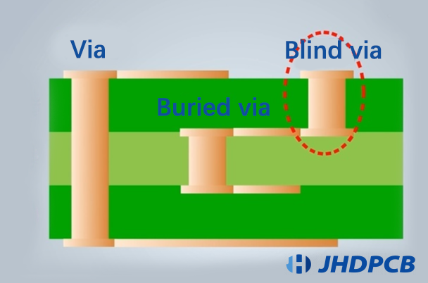
Beyond that above, we have to know there are three common types of vias, including plated through-hole, buried hole, and blind hole. Then detailed information about these three vias will be offered to you.
- Plating through holes-
Plating through holes is the most frequent via. The judgment criteria of being seen as a PTH is that you can see light when you raise up the PCB and face to the light. PTH has the simplest fabrication, it can be finished only by drilling a full hole or making a full hole through laser light. In addition to this, the cost of PTH is relatively inexpensive. But in some circumstances, plating through holes are not needed for some circuit layers. The reason is that PTH will take up more space even with cheaper costs. - Blind Via Hole(BVH)-
As its name suggested, blind via holes reveals that the opposite cannot be seen when the adjacent inner layer and the outermost circuit of the PCB are connected by a plated through-hole.
The main advantage of BVH is to improve the utilization rate of space for PCB circuit layer. But the depth of the hole is the most vital thing you should pay attention to. The z axis( the depth of the hole) should be suitable. This production method can merely be used because of the difficulty of hole plating. - Buried Via Hole (BVH)-
Buried via holes can connect the PCB’s any circuit layers except the outermost layer. This process must be finished in a complex way. The first step is you need to carry out the internal bonding after the plating treatment when other individual circuit layers are drilled. Then the all is bonded. The cost of Buried via holes is the most expensive because of its longer fabrication time than blind via holes and through holes. This product method can be employed in HDI (high-density) circuit boards in order to add more available space for other circuit layers.
Click to view more detailed PCB hole type information.
As a result, you totally need to use printed circuit boards with plated through holes, if you are expected to have a high-efficiency electronic product. But, to be honest, there certainly exists some risks.
The problem of thermal cycling will impact all products with printed circuit boards. They will consistently heat up when we charge them up. This condition will last until they are cut down, which is the time to cool down. The temperature will increase together with the temperature rising of the product. The risk of cracking will ascend as the repeated process of heating up and cooling down. The PCB hole plating thickness of copper plating determines the time of thermal cycling. Namely, the thicker the copper is, the longer it can persist. The service life of the printed circuit board is inextricably bound up with the thickness of copper plating inside the through hole because the failure of boards is directly resulted by this cracking.
Drilling tolerance
It’ ‘s needed for standard plated through holes that the finished hole size is smaller about 0.006” than the drilled hole size. This can facilitate copper from 0.0008” to 0.001” to be plated inside the hole.
The drilling tolerance can be caused by two reasons. The first one is the long-term used drill bit is not as sharp as a new drill bit and the size of the old drill bit is no longer a standard size. Some cases may occur when one of the three stacked panels shifts a little, including the not nominal drill size, the drill misregistration, and the process of the head moving up and down.
Routing tolerance
The tolerance of routing has a greater tolerance than the drilling process. The routing tolerance is caused by the tolerance of the router bit itself and the track deviation of router bits.
If a 0.250” finished plated hole is needed by a PCB circuit board, a 0.256” diameter opening is required to be created by the router for plated holes. For the 0.256” diameter opening, the tolerance of itself is +/-0.004. under this circumstance, it’s the perfect status for the finished 0.250” size that the tolerance is +/-0.005. Beyond that, the process has two variables, one is chemistry, the other one is the faster plating speed of smaller holes than bigger holes in most cases.
Chemical Plating tolerance
As the copper plating process, the size of the hole will lessen and then equal to the finished size. It’s impossible for the current technology to realize a +/-0.001” tolerance. The +/-0.003” tolerance is the most suitable choice for holes with sizes up to 0.249”.
The process of copper plating is determined by three factors, including the amps of current sent into circuit boards, the temperature of the tanks, and the time of circuit boards in the plating tanks. For a standard plating process, it requires 45 minutes to an hour to plate enough copper inside the hole. The size of the plating hole tolerance is caused by time in the plating tanks, the amps involved, the chemistry variables, and the temperature of the tanks. Affected by these factors, the size tolerance of finished plated holes is +/-0.003”.
For press fit holes, in order to achieve a tight fit between components and the hole, the perfect tolerance of them is +/-0.002”, which is the strict tolerance required by the plating department. IPC 0.0007 mils are the first choice for holes under this tolerance. And in this way, those press-fit holes can be easily plated within +/-0.002” tolerance. And all the +/-0.003” holes will be within the tolerance. Because of the required longer time of panels staying in plating tanks, it’s harder to achieve the plating tolerance is within +/-0.002”, when a 0.001” minimum size is required by customers.
Slots And Cutouts tolerance
A big plating nightmare will be caused by a drill chart that requires a tolerance is +/-0.003” for plated holes and have big cutout plated ares and slots with a tolerance of only +/-0.003”. The large plated cutouts are at the upper end of the tolerance under the condition of +/-0.002” holes being plated to the finished required size of +/-0.002”. As a result, all the cutouts and holes can be nominal finished sizes when the holes tolerances are +/-0.003” and the slots and cutouts tolerances are +/-0.005”.


