HDI PCB
With the development of high-density, high-precision electronic products, the market demand for HDI PCB is also increasing. HDI PCBs enable more functional interconnects in a smaller board area. This enables PCB miniaturization for many applications, but of course it also presents difficulties in HDI PCB production. JHDPCB is specially equipped with a full set of state-of-the-art production lines for HDI products, and is equipped with a full set of surface treatment equipment (Immersion Gold, Immersion Silver, Immersion Tin, OSP, Spray Tin, Gold Plated Thick Gold Plated, Tin Plated, Silver Plated). Batches of 2-12 Layer HDI PCB, production minimum line width and line spacing 40um/40um. For more information about our process capabilities, please refer to our HDI Capcity. Next we will take you to learn more about HDI.

What is HDI PCB?
High-density interconnects (HDI) are PCBs with a greater number of interconnects and a minimal footprint. This leads to miniaturization of the circuit board. The components are placed closer together, and the board space is significantly reduced, but the function is not affected.
More precisely, a PCB with an average of 120 to 160 pins per square inch is considered an HDI PCB. HDI design combines dense component placement and veratile routing. The HDI popularized microvias technology. Through the implementation of microvias, buried vias and blind vias to make more dense circuits. The microvias, buried vias and blind vias of HDI PCB all need to be produced by laser drilling machine. The precision of the laser drilling machine determines the quality and precision of the vias produced. JHDPCB has 60 sets of Japan’s Mitsubishi laser drilling machines, through the start of Synchrom technology, to achieve high-capacity processing. The minimum aperture of laser holes can reach 0.06mm.

What are the advantages of HDI PCBs?
· Compact design
The combination of microvias, blind vias, and buried vias greatly reduces board space. With the support of HDI technology, it is possible to achieve twice the functionality of a standard PCB in the same size. Thereby reducing the PCB size to accommodate more applications.
· Excellent signal integrity
HDI utilizes via-in-pad and blind via technologies, which help bring components close to each other, reducing signal path lengths. HDI By using small vias, all stray capacitances and inductances are reduced. At the same time, the via stubs are removed, thus reducing the reflection of the signal, thereby improving the signal quality. These will result in faster signal transmission and better signal quality. JHDPCB adopts high-precision back-drilling technology to reduce the equivalent series inductance of vias and meet the integrity requirements of product signal transmission.
· High reliability
The implementation of stacked vias used by HDI technology enables these boards to withstand extreme environmental conditions. Provides better durability and reliability for PCBs in hazardous conditions and extreme environments.
· High cost performance
If the traditional pressing process is used, when the board layer exceeds 8 layers, more manufacturing costs are required. But HDI technology can reduce the functionality of a standard 8-layer PCB to a 6-layer HDI board (or even less) without compromising quality. Maintain the desired functionality while reducing cost. JHDPCB can mass produce 4-12 layers, 3-level HDI, and the price is very cost-effective.
Our advantages in HDI PCBs.
The world’s leading production equipments:We have introduced a variety of world-renowned production equipment, such as Orbotech LDI, VIGOR lamination machines, Mitsubishi laser drilling machines, Command plating lines, PTH Lines and etc.
Excellent procurement supply chain management: We reduce our material costs through centralized procurement and large-scale procurement.
Experienced team of experts: We have been deeply engaged in HDI PCBs production for more than 12 years and grow into an industry-leading HDI PCBs manufacturer, supported by an experienced team of experts that can provide our customers with reliable quality HDI PCB.
Quick delivery: To shorten the delivery time. Everything is manufactured under one roof with our state-of-the-art equipment. We have many brands of laminate in stock, such as aluminum. See ‘CCL Types’ for more sheet information. Can deliver 3-5 days for sample order and 14-18 days for bulk order. More lead times can be found in “PCB Quick Turn“.
Rich experience in projects: Over the years, we have served various HDI projects in various industries, and manufactured the highest quality HDI PCB projects for virtually every technology company, and we can do the same for you.
JHD HDIPCB detailed manufacturing capabilities.
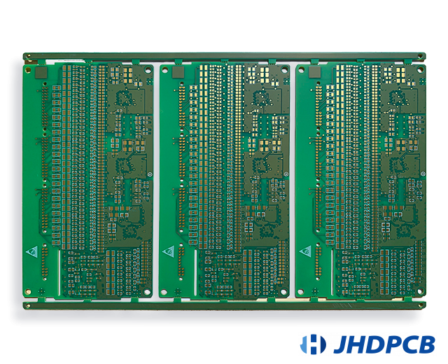
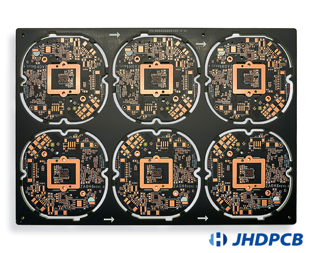
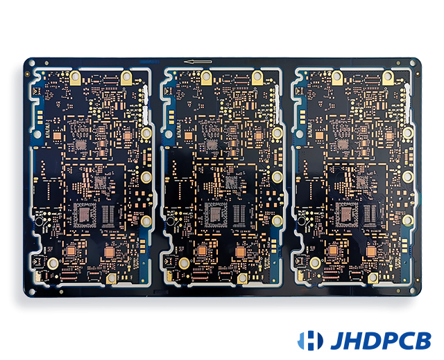
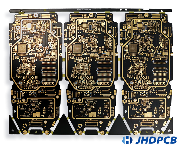
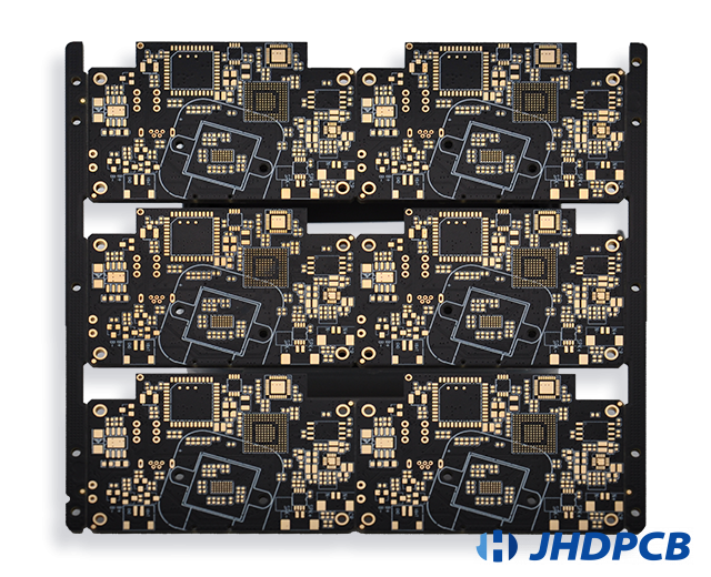
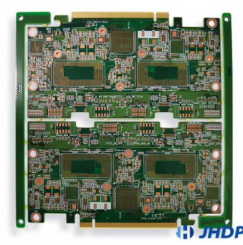
JHDPCB related HDI product case show:
The difference between HDI and standard PCBs
| HDI PCB | Standard (Through-hole) PCB |
|---|---|
| Higher component density | Lesser compared to HDI |
| Smaller, lighter boards with more functionality | Larger and heavier boards |
| Implementation of Blind, buried, and microvias | Through-holes |
| Laser direct drilling | Mechanical drilling |
| Lower number of layers | Higher number of layers |
| Compatible with high pin count and low pitch packages | May face compatibility issues with low pitch packages |
What are the applications of HDI PCBs?
Smartphones and Tablets:
All smart phones are HDI PCBs with ELIC (Each Layer Interconnect) structure. HDI PCBS are responsible for making thinner and smaller portable electronic devices.
Automotive:
Automakers love small PCBs because they save more space inside the car. With the introduction of intelligent assistance functions such as new energy and intelligent assisted driving in recent years, integrating electronic devices to provide a better driving experience has been a major focus of automakers. Then a series of high-tech automotive sensors need a suitable PCB support.
Health Care:
One of the most critical areas where high-density PCBs are making great strides is in the medical field. Medical devices often require small packages with high transmission rates that only HDI PCBs can provide. They can be installed in small devices such as implants, laboratories and imaging equipment. The small enough size and excellent signal transmission of HDI play a vital role for doctors in diagnosing diseases. Medical equipment plays a vital role in diagnosing diseases, and it does provide life support.
Wearable Technology:
With the introduction of other wearable devices such as Apple Watch and VR headsets, HDI is becoming a major stakeholder in the consumer market. Due to its exceptional functionality, wearable technology is becoming more and more popular among young people.
Military And Aerospace:
HDI is incorporated into military communications device and other strategic equipment such as missiles and defense systems. The HDI PCBs are well suited for extreme environments and hazardous conditions, making it ideal for aerospace and military applications.
| HDI Structures | Type of Micro vias | Mass Production | Small-Middle Batch | Prototype | Available |
|---|---|---|---|---|---|
| 1+N+1 | Blind vias | Yes | Yes | Yes | 4 layers+ |
| 2+N+2 | Blind/Buried staggered vias | Yes | Yes | Yes | 6 layers+ |
| 2+N+2 | Blind/Buried stacked vias | Yes | Yes | Yes | 6 layers+ |
| 3+N+3 | Blind/Buried staggered vias | / | Yes | Yes | 8 layers+ |
| 3+N+3 | Blind/Buried stacked vias | / | / | Yes | 8 layers+ |
The birth of HDI PCB has brought more diversity to all digital electronic devices and also brought more challenges to PCB manufacturers. In order to adapt to the trend of miniaturization and multi-functionalization of electronic products, JHDPCB has done a lot of work for the professionalism of employees while introducing first-class precision equipment. We will use our professionalism and ingenuity to provide you with satisfactory service and HDI products. As a top 5 PCB manufacturer in China. JHDPCB is trustworthy and experienced. Just contact us and send your Gerber file and request for material and quantity and we will give a price shortly.
We also offer a free PCB file check to help you get the correct PCB design before full production and avoid costly mistakes. Our services are all IPC Class 3 compliant, all designers comply with ISO9001:2015 quality management system, our in-house quality control department will verify that your prototype meets our and your high standards before we send it to you .
JHD takes high-quality as the foundation, technology research and development as the engine, and customer satisfaction as the center. Hold high-efficiency and high-quality delivery as mission, strives for perfection.
JHD believes that the attitude to customers determines the height of the enterprise. We require accuracy on each point.
Quality is life and delivery schedule is important for reputation. JHD always adheres to on-time delivery, has established a good brand in the industry.


