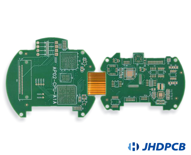
HDI PCB is one of the fastest growing technologies in the PCB industry today. It has higher circuit density than standard PCBs, HDI PCB designs can include finer lines and spaces, smaller vias and capture pads, and higher connection pad densities. With some sophisticated techniques, more functional interconnects can be achieved in a smaller board area. This enables PCB miniaturization for many applications.
Usually, the hole diameter of HDI PCB is less than 6mil, the hole diameter (HolePad) is less than 0.25mm, the contact density is more than 130 points/square inch, and the wiring density is more than 117 inches/square inch. In addition, line width/spacing below 3mil/3mil. HDI PCB create denser circuits by implementing micro, buried, and blind vias, typically containing vias 0.06mm in diameter or smaller.
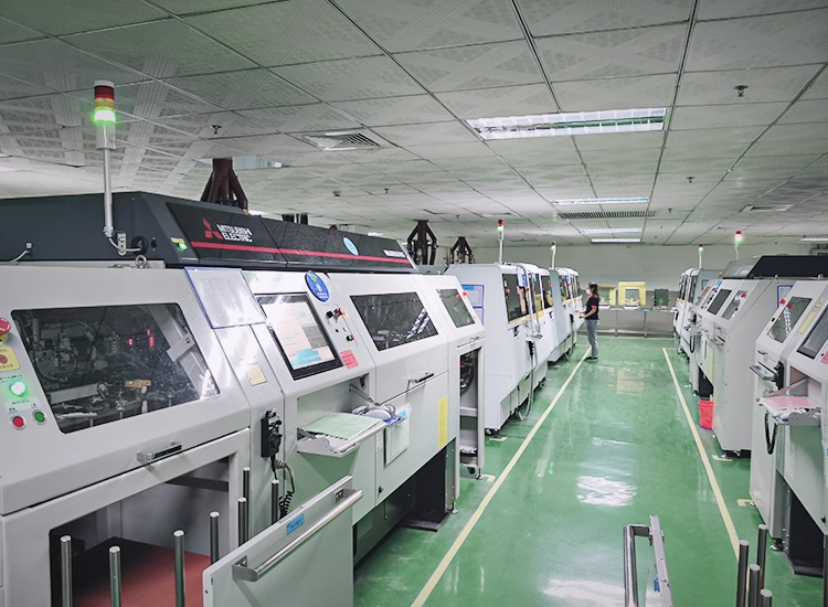
JHDPCB has 60 sets of laser drilling machines from Japan Mitsubishi ML605GTW6-H. Through the start of synchronous technology, large-capacity processing of HDI PCB can be realized, and the minimum diameter of laser holes can reach 0.06mm.
HDI PCB is generally manufactured by the lamination method. The more the number of laminations, the higher the technical grade of the board. Ordinary HDI PCB are basically one-time stackup, and high-end HDI PCB uses two or more stackup technologies, while using advanced PCB technologies such as stacking, electroplating, and laser direct drilling. When the layers of the PCB more than 8 layers, the cost of using HDI PCB will be lower than that of the traditional complex lamination process.
The electrical performance and signal accuracy of HDI PCB are higher than standard PCBs. In addition, the HDI PCB has better improvements for frequency effects, radio wave effects, electrostatic induction release, and heat conduction. High Density Integration (HDI) technology enables more miniaturization of terminal equipment design products, and achieves more standardization of electronic device characteristics and high efficiency.
The HDI board uses the buried hole electroplating process and then carries out secondary pressing, which is divided into first-step, second- step, third- step, fourth- step, and fifth- step. The more step, the more difficult the HDI is to produce. At present, the HDI technology selected by JHDPCB has increased the number of top layers to 20 layers; maximum 7 steps; the minimum diameter is 0.06 mm.
By using HDI technology, HDI PCBs have thinner lines, smaller holes and higher density than standard PCBs. At the same time, HDI offers better signal integrity performance than standard PCBs because all stray capacitance and inductance are reduced when using small blind and buried vias. The stray capacitance of regular PCB vias is much higher, which results in larger impedance discontinuities than microvias. On the other hand, since HDI has no stubs, the impedance of the microvia is close to the trace impedance. It allows designers to combine dense component layouts with finer circuits. This means faster signal transmission, significantly lower signal loss and crossover delay.
With the development of HDI technology, engineers have gained a very free and flexible design direction. Designers can now place more components on both sides of the original PCB as needed. HDI PCBs use laser drilling, while traditional PCBs usually use mechanical drilling. Laser drilling allows for smaller apertures, ranging in size from 3.0-6.0mil, which can save a lot of pad space and enable more layout per unit area.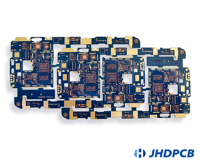
Generally speaking, HDI PCB have the following advantages:
It can reduce the cost of PCB:
When the density of the PCB increases beyond the 8 layers and manufactured with HDI technology, the cost will be lower than the traditional complex lamination process.
Increase The Circuit Density:
The interconnection between traditional circuit boards and parts must be connected through the lines and through-hole conductors drawn around the QFP (fan-in and fan-out methods), so these lines need to occupy some space. The microvia technology can hide the wiring required for interconnection to the next layer, and the connection between the pads and the leads between the different layers is directly connected by the blind vias in the pads, without fan-in and fan-out wiring. Therefore, some solder pads (such as mini-BGA or CSP small ball soldering) can be placed on the outer layer board to accept more parts, which can increase the density of the circuit board. This new stacking and wiring method is used in many mobile phone boards of high-performance small wireless phones. JHDPCB can produce minimum BGA pad 8 mil and minimum BGA pitch 8 mil.
Conducive To The Use Of Advanced Assembly Technology:
Generally, traditional drilling technology cannot meet the needs of small parts of the new generation of thin lines due to the size of the pads (through holes) and mechanical drilling. With the advancement of microvia technology, designers can design the latest high-density IC packaging technologies, such as matrix packaging (Array package), CSP and DCA (Direct Chip Attach), into the system.
Have Better Electrical Performance And Signal Accuracy:
In addition to reducing signal reflection and crosstalk interference between lines, the use of micro-via interconnection can increase more space for circuit board design. The physical structure property is that the holes are small and short, so the effect of inductance and capacitance can be reduced, and the switching noise during signal transmission can also be reduced.
Better Reliability:
The micro-hole has a thinner thickness and a 1:1 aspect ratio, so the reliability of the signal transmission is higher than that of the general through-hole.
Can Improve Thermal Properties:
The insulating dielectric material of HDI board has a higher glass transition temperature (Tg), so it has better thermal properties. Understand the characteristics of high TGPCB;
Can Improve Radio Frequency Interference/Electromagnetic Wave Interference/Electrostatic Discharge (RFI/EMI/ESD):
Micro-hole technology allows circuit board designers to shorten the distance between the ground layer and the signal layer to reduce radio frequency interference and electromagnetic wave interference; on the other hand, it can Increase the number of grounding wires to avoid damage to parts in the circuit due to instantaneous discharge caused by electrostatic accumulation.
Improve Design Efficiency:
Micro-via technology can allow the circuit to be arranged in the inner layer, so that circuit designers have more design space, so the efficiency of circuit design can be higher.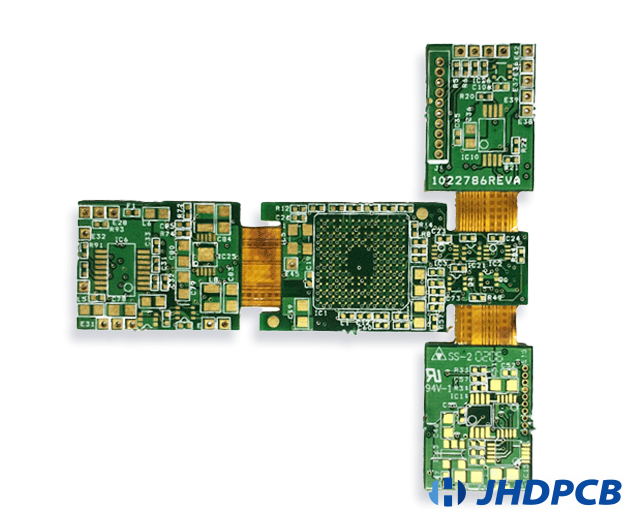
Due to the design flexibility and tiny size of HDI PCBs, and faster model transfer performance. HDI PCBs have a very wide range of applications, and they can be found in digital devices such as smartphones, automobiles, medical equipment, life electronics, and military aerospace.
Automotive:
Automakers love small PCBs because they save more space inside the car. With the introduction of intelligent assistance functions such as new energy and intelligent assisted driving in recent years, integrating electronic devices to provide a better driving experience has been a major focus of automakers. Then a series of high-tech automotive sensors need a suitable PCB support.
Health Care:
One of the most critical areas where high-density PCBs are making great strides is in the medical field. Medical devices often require small packages with high transmission rates that only HDI PCBs can provide. They can be installed in small devices such as implants, laboratories and imaging equipment. The small enough size and excellent signal transmission of HDI play a vital role for doctors in diagnosing diseases.
Photography Skill:
More miniaturized cameras are born with HDI PCB technology. But image quality didn’t suffer. This allows photography enthusiasts not to carry bulky equipment all the time.
Smartphones and Tablets:
All smartphones are HDI PCBs with ELIC (Interconnect per Layer) structure. HDI PCB is responsible for making thinner and smaller portable electronic devices.
Wearable Technology:
With the introduction of phone watches and other wearables such as VR headsets, HDI is becoming a major stakeholder in the consumer market. Wearable technology is gaining popularity among the younger crowd due to its superior functionality.
Military and Aerospace:
HDI is incorporated into military communications equipment and other strategic equipment such as missiles and defense systems. HDI PCBs are ideal for extreme environments and hazardous conditions, making them ideal for aerospace and military applications.
The possibilities for future high-density interconnect PCB technology seem almost limitless. No matter what industry you’re in, you probably already have some ideas about how high-density interconnect PCBs can help make the electronics you make or use better. The birth of HDI PCB has brought more diversity to all digital electronic devices and also brought more challenges to PCB manufacturers. In order to adapt to the trend of miniaturization and multi-functionalization of electronic products, JHDPCB has done a lot of work for the professionalism of employees while introducing first-class precision equipment. We will use our professionalism and ingenuity to provide you with satisfactory service and HDI products.
Learn more about the advantages of jhd in HDI PCB.


