BGA package

directory

What is BGA Package?

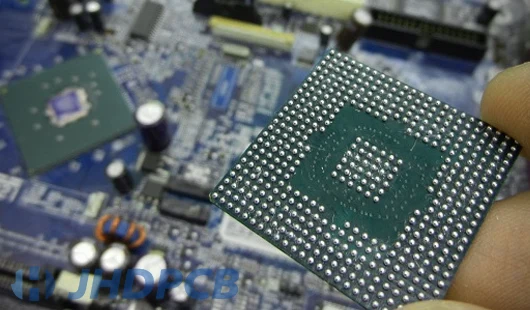
A Ball Grid Array or BGA is a surface mount package (SMD component) without leads. We often use this type of surface mount packaging for surface mount technology (SMT) and utilize the metal balls of solder balls for electrical connections so that the BGA solder balls are attached to the laminate substrate on the bottom of the package. However, the die attach of the BGA to the substrate is by wire bonding or flip-chip technology. BGA substrates have internal conductive traces that are used to route and connect die-to-substrate bonds to substrate-to-ball array bonds. Similar to it is CSP chip-scale package.

BGA-assembly

What are the Common Types of BGA Package?

Different BGA assembly manufacturers in different countries use different types of BGA package processes in the package process. Below I will detail the most popular and widely used BGAs, including: PBGA (Plastic Ball Grid Array), CBGA (Ceramic Ball Grid Array), TBGA (Tape Ball Grid Array), EBGA (Enhanced Ball Grid Array), FC-BGA (Flip Chip Ball Grid Array), MBGA (Metal Ball Grid Array), Micro BGA,MAPBGA and TEPBGA,etc.

PBGA (Plastic Ball Grid Array):

The first to introduce is our PBGA, which is the abbreviation of Plastic Ball Grid Array. This is the most popular type of double-sided PCB cap used recently. It was invented by Motorola and is now widely used by most manufacturers. Its core is bismaleimide triazine (BT) resin as the base material. Combined with the application of overmolded pad array carrier (OMPAC) packaging technology or ball-to-pad array carrier (GTPAC), it is highly reliable and JEDEC (Level 3) qualified. This BGA can carry an array of around 200 to 500 balls and is suitable for a large number of applications. We JHD can use this technology for double-sided bga assembly, making our electronic boards more environmentally friendly, longer lasting, more heat dissipation, and high fire resistance.

Plastic Ball Grid Array

CBGA (Ceramic Ball Grid Array):

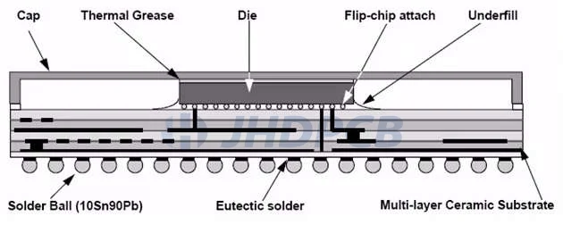
The next thing we want to introduce is our ceramic BGA. In this type, the ratio of tin to lead is 10:90. This type of BGA has a high melting point and requires the C4 method (Controlled Collapse Chip Connection) to bridge between the BGA and the PCB. The cost is a little higher than PBGA, but BGA is more reliable, has better electrical performance and better thermal conductivity.

CBGA

TBGA (Tape Ball Grid Array):

The third introduction to you is TBGA. Its only downside is that its cost is always higher than PBGA. However, if a thin product is to be made, it should have a strong core, better heat dissipation and highest electrical connection performance. Definitely TBGA’s choice. Does the IC/chip have to face up/down; this is how to make the product value for money while keeping costs optimal. If the chip is up, wire bonding is recommended, and when the chip is down, the flip-chip approach is recommended in such BGAs.

TBGA

EBGA (Enhanced Ball Grid Array):

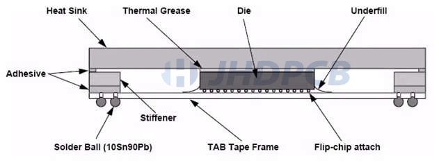
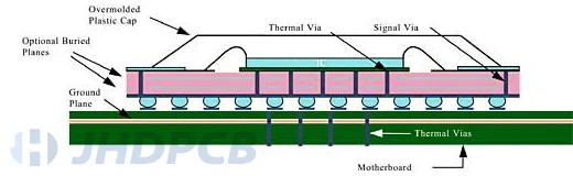
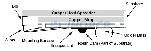
The fourth is our Enhanced Ball Grid Array, which is the sum of the PBGA and additional heatsink options. A dam is built at the boundary around the electronic components/chips on the substrate and a liquid compound is added to seal the components on it. In this type, the chip is always facing down and wire bonds are used to conduct electricity between the PCB and the chip used.

EBGA

FC-BGA (Flip Chip Ball Grid Array):

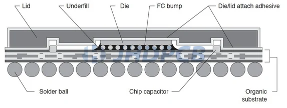
Next is the flip chip ball grid array, which is absolutely similar to CBGA, the only difference is the ceramic substrate. On the contrary, BT resin is used in FC BGA, which saves additional cost. Its main value lies in a shorter electrical path than any other BGA type and results in better conductivity and faster performance. In this BGA, the ratio of tin to lead is 63:37. Another advantage of this BGA is that the chips used on the substrate can be re-aligned into the correct position without the need for a flip-chip aligner approach.
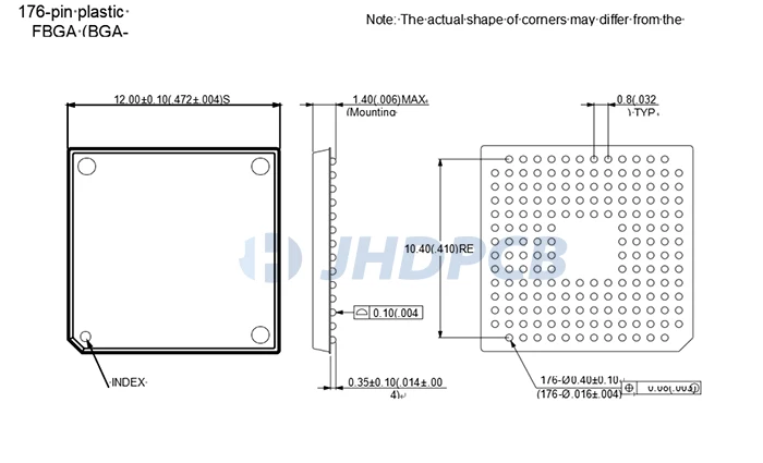
FC-BGA

MBGA (Metal Ball Grid Array):

The cermet is used as the substrate in the metal ball grid array type .In this method, the chip is face down and the circuit consists of this sputtered coating. In this method, wire bonds are used to make connections. This array is ideal for very good electrical performance and better heat dissipation values.

Mmicro BGA Package:

Finally, we want to introduce the Micro BGA. In this method, the chip is always face down, while the substrate consists of packaging tape. The value is that it uses an elastomer between the tape and the chip, which creates thermal expansion stress. Micro BGAs’ most important value is their naming, mini size. Therefore, bga assembly factories are allowed to plan high-tech but small products. Most importantly, this type is at the heart of higher memory products with low pin counts. Therefore, better accessibility reduces liability at the same time.

MAPBGA(Moulded Array Process Ball Grid Array):

This BGA package provides a low-cost option with a small footprint and high reliability for low-to-mid-performance devices requiring a low-inductance package that is easy to surface mount.

TEP BGA(Thermally Enhanced Plastic Ball Grid Array):

This TEP BGA package provides a higher level of heat dissipation. It draws heat from the chip to the customer board by using thick copper layers in the substrate. It is widely used on thick copper PCB.

Advantages and disadvantages of BGA assembly technology.

Advantages of BGA Packages:

1. High Interconnect Density
The first and most important advantage of BGA packaging is its high interconnect density. The end space of the BGA packaging process is very large. So the available connection density is higher, allowing more I/O ports. It can help HDI PCB to achieve better precision interconnection of circuits.
2. Small footprint
BGA packages take up less space on the printed circuit board.Assembling a ball grid array to a circuit board is more efficient and more manageable than leaded electronics because the solder needed to solder the package to the circuit board comes from the solder balls themselves. These solder balls also “self-align” during installation.
3. Having Better Heat Dissipation
The lower thermal resistance between the BGA PCB packages and the bga pcb assembly is another advantage of this package. The lower the resistance, the better the heat dissipation. This allows heat to flow more freely, allowing for better heat dissipation and avoiding high chip temperatures. In order to prevent the device from overheating and affecting normal use.
4. Better Conductivity
Due to the lower inductance of the BGA package. So BGA package produces smaller solder joints and shorter leads. This makes the BGA provide better conductivity. Effectively avoid signal distortion in high frequency PCB applications. Therefore, BGA packages have more stable electrical and frequency transmission in high frequency circuit boards.
5. Increased Performance
The BGA packaging process has lower solder defects and stronger solder joints. And can freely adjust the tension between the solder joints, resulting in an excellent custom center effect. Compared with other IC packaging technologies, all of these factors ultimately give ball grid arrays better electrical performance. The bump technology is combined with appropriate BGA substrate materials to make it have excellent performance at high speed.

Drawbacks of BGA package

Of course, everything has two sides. In addition to its advantages, BGA also has some disadvantages.

  1. More Susceptible to Stress:
    BGA packages are more susceptible to stress, as the flexural stress of the circuit board can lead to potential reliability issues.
  2. Inconvenient to Check:
    Once the BGA is soldered to the board, it can be difficult to inspect for defects in solder balls and solder joints.
  3. A little expensive:
    In fact, in IC packaging, the cost of IC packaging solution is relatively low, but the use of BGA packaging process will make the cost relatively high. For example, compared with QFN package, BGA package process adds bump process and substrate, which is the factor of cost increase.

How to Solder BGA Package?

BGA assembly is one of the key issues when introducing BGAs. Since the pads cannot be accessed in the normal way, BGA components will be up to a standard that can be achieved with more traditional SMT packages. In fact, while soldering appears to be a problem for ball grid array BGA devices, we have found that standard reflow soldering methods work for these devices with excellent connection reliability. Since then, BGA assembly methods have improved and BGA package soldering is generally considered particularly reliable.
During welding, the whole components are heated. Solder balls have a very strictly controlled amount of solder, which will melt when heated during welding. The surface tension allows the melted solder to maintain the correct alignment of the package with the circuit board as the solder cools and solidifies. The composition of the solder alloy and the welding temperature are carefully selected so that the solder will not completely melt, but remain semi liquid, separating each solder ball from its adjacent solder balls.
Since many products now adopt BGA packaging as the standard, the BGA assembly method is now perfect and can be easily adopted by most manufacturers. Therefore, there should be no fear of using BGA devices in the design.

Reflow soldering is commonly used in soldering BGAs because it helps heat the entire PCB components to a fixed temperature to melt the solder or solder balls underneath the BGA assembly.
For any BGA welding, the solder ball on the package has a controllable amount of solder. Solder balls of various bga package sizes such as 18 mil, 24 mil and 30 mil can be provided.

 When a circuit board with solder balls and BGA packages is placed in a reflow furnace, it will be heated and the solder will melt. The surface tension keeps the melted solder properly aligned with the circuit board. It is important to pay attention to the composition of the solder alloy and the welding temperature, so that the solder will not completely melt, but remain semi-solid, so that the solder balls are separated from each other and will not lead to any bridging.

Similarly, hot air is the most common way to weld BGA. The following are the steps of using hot air to weld BGA packages:

  1. After removing the BGA package, clean the pad and remove the excess solder on the board.
  2. Pay special attention to applying flux paste, not liquid flux, to the pads. Solder paste flux can help the solder balls adhere more firmly so they don’t fall off or change position.
  3. Carefully place the solder balls on the pads.
  4. Apply flux to the bottom of the BGA package, where we call it the solder surface.
  5. Carefully and patiently place the BGA package on the solder balls.
  6. Preheat, then blow hot air from the top and bottom with a hot air blower.
  7. The solder balls will be melted and soldered by the hot air.

If the correct procedure is used to complete BGA technology and BGA welding, it is very reliable. BGA has low heat resistance, so there is little or no damage due to overheating.

One of the many problems of BGA equipment is the inability to use optical methods to view welded connections. Therefore, when the technology was first introduced, people raised some doubts. In order to ensure that they can weld the equipment satisfactorily, many manufacturers have conducted many tests. Sufficient heat must be applied to weld the BGA device, which is to ensure that all the balls in the grid are fully melted. So that each joint can be manufactured satisfactorily.
The connector cannot be completely tested by checking the electrical performance. There are two reasons: one is that the joint may not be fully manufactured, and the other is that it will fail over time. However, the only satisfactory examination method is the use of X-ray examination. Because this inspection method can observe the solder joints below through the equipment. As long as the heat distribution of the soldering machine is found to be set correctly, BGA device soldering will hardly encounter any problems. This makes it suitable for most applications.

Unless there is the right equipment, it is not easy to rework the circuit board containing BGA as we expected. If you suspect that the BGA circuit board is faulty, you can remove the device to judge. Because the circuit board is realized by locally heating the equipment to melt the equipment solder under it.
During the repair of BGA circuit boards, heating is usually eliminated in the repair station, including a fixture equipped with an infrared heater, a thermocouple for monitoring temperature and a vacuum device for lifting packaging. We need to be very careful to ensure that only BGA is heated and removed. Try to minimize the impact on other nearby equipment, otherwise they may be damaged.

After the BGA circuit board is removed, we can replace it with a new one. Sometimes the removed BGA circuit board can be refurbished or repaired. If the BGA chip is expensive and still works after removal, then this BGA repair may be an attractive proposal. During BGA maintenance, we need to replace the solder balls and use some small solder balls for re welding.
Many PCB Assembly Factory have established special equipment to carry out such BGA reballing.

What are the basic rules that the BGA packaging process should follow?

When we carry out BGA packaging, we should pay attention to the following aspects:

  1. Sufficient heat must be applied to ensure that all the balls in the grid are fully melted and that each BGA Solder joint is firmly bonded.
  2. Until the solder cools and solidifies, the surface tension of the molten ball is to facilitate the package fixed on the PCB. What is necessary for solid solder joints and preventing solder balls from short circuiting each other is the optimal temperature-controlled BGA welding process.
  3. Both the composition of the solder alloy and the welding temperature are precisely selected, so that the solder will not completely melt, but will remain semi-liquid, and each ball will remain separated from its adjacent ball.
  4. Damage: the pins on QFP are very thin, and their spacing needs to be tightly controlled. Therefore, any improper handling may lead to failure, and when this happens, the tragedy will be irreparable. The main problem is that IC with high pin count is often very expensive.
  5. Pin density: From the point of view of the bga package design, the pin density leads to the following problems: first, it causes problems in moving the wiring from the IC; second, congestion may occur in some areas.
  6. Welding process: since the spacing between QFP pins is very small, we need to control the welding process very carefully to avoid contact bridging. Make sure there are no solder balls on the BGA solder joints. Ensure that the boundary of BGA solder joints is clear, smooth and clean, and there is no gap. The size, volume, grayscale and other shape features of all solder joints are uniform and aligned.
  7. Strictly implement the inspection process: The most commonly used inspection methods for BGA inspection include AOI inspection and automatic X-ray inspection. However, due to the difference in welding technology and equipment used. It is necessary to choose other different detection methods according to the actual situation. Click to view complete PCB testing knowledge.
    Common BGA inspection problems include defects such as missing solder balls, misalignment, loose solder, opens, bridges, cavities, and uneven dimensions.

BGA Package Datasheet.

FUJITSU SEMICONDUCTOR DATASHEETBALL GRID ARRAY PACKAGE
176 PIN PLASTIC
BGA-176P-M01To Top / Package Lineup / Package Index
176-pin plastic FBGA
(BGA-176P-M01)
Ball pitch: 0.80 mm
Ball matrix: 14
Sealing method: Plastic mold
BGA-176P-M01

*The contents of this document are subject to change without notice.
We suggest you consult our JHDPCB’s sales representative before ordering.
We will not be liable for any infringement of patent rights or other rights of third parties arising from the use of the information in this document or the package size.
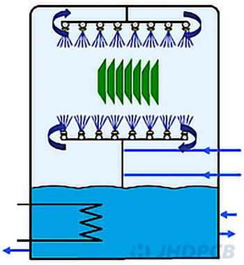
As shown in the following table, the different pitches available in the BGA package have been listed.
BGA pins ball Pitch in mm Signal layer counts
2 trace 1 trace
256 1 2 3
324 0.8 2 3
484 0.8 3 4
484 1 2 4
625 0.8 3 4
676 1 3 5
784 0.8 4 5
900 1 3 5
1156 1 3 6
1517 1 4 7
1760 1 4 8
1924 1 4 8
2577 1 5 9
2892 1 5 10

How to Clean BGA Packages?

Due to different process requirements, we can use a variety of cleaning machinery and cleaning equipment.

The working principle of the single chamber spray system is the same as that of the bowl machine. All processing steps will be performed in the same processing room. The machine can spray the cleaning medium onto the electronic components for cleaning through the nozzle assembly or rotating the spray arm. The cleaning effect is usually achieved not by the ejection pressure but by the volume of the cleaning medium of the substrate.
This type of machine is suitable for small and medium-sized production speeds, and it takes up less space in the production area.
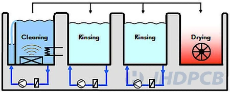
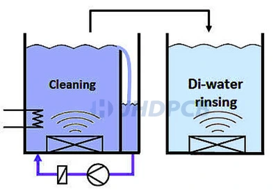
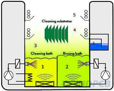
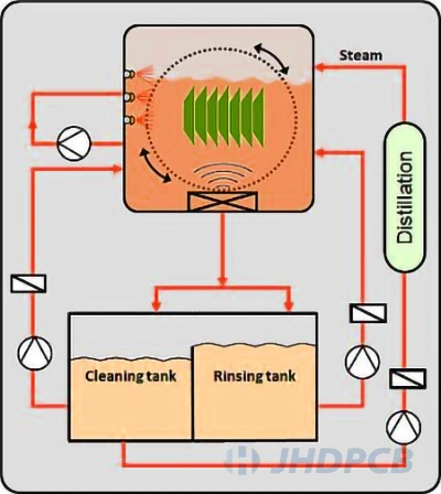
Spraying Mechanism

In the immersion tank cleaning system, components, templates, pads, machine parts and so on usually need to go through several cleaning stages, in which separate cleaning, rinsing and drying steps are required. Compared with the single chamber spray system, the agitation of cleaning medium in the immersion tank cleaning system is realized by ultrasonic wave or immersion spray system.
In addition to our commonly used water-based cleaners, another type of flux that can be used in immersion cleaning systems is modern solvent based cleaners with high flash points. When the cleaning materials are transferred from one process step to the next, the part throughput determines whether to use manual or automatic.

Immersion Tank Mechanism

It is well known that the propagation of pressure and density fluctuations (compression and sparsity of molecules) in elastic media forms sound. The frequency from 20 Hz to 20 kHz is the range that humans can hear. The vibration that exceeds the maximum frequency that humans can hear is usually called ultrasound.
The frequency range 35 kHz to 45 kHz is a typical cleaning frequency range.In the cleaning tank, the ultrasonic transducer elements in the cleaning tank propagate underinflation and overpressure waves. In order to remove the dirt particles on the surface, cavitation generates pressure jets (micro jets) to achieve this purpose.
Because the acoustic wave can reach every angle where the circuit board is installed, ultrasonic cleaning is useful both under cleaning components and in complex geometries.In order to prevent “hot spots” from cleaning materials, most cleaning machines have an automatic frequency adjustment function, which is used to modulate the working frequency of ultrasound (scanning).
According to mil-std-2000 Rev. A and j-std-001, we can test that the use of ultrasound in electronic cleaning is allowed. However, we carry out the test procedure before applying ultrasonic wave to electronic components.

Ultrasonic Cleaning Mechanism

If a shorter process, drying time and anhydrous cleaning is required, a modern HFE cosolvent cleaning process can be selected. We usually use it in the military and aerospace fields.
HFE (hydrofluoroether) is nonflammable, non-conductive, fast drying and residue free, and is developed as a substitute for CFC or similar solvents.
HFE is used in the cleaning bath together with the cosolvent, and immersion spray or ultrasonic stirring is used to dissolve the persistent residue. The flushing step is only carried out in the HFE bath, followed by steam flushing. Finally, in order to dry PCBs, we need to use strong cooling. In order to prevent HFE evaporation, the process must be carried out in a washing machine with efficient cooling technology.

HFE Cosolvent Mechanism

One chamber vacuum cleaning is only applicable to solvent. When drying in a vacuum environment, the cleaner is sprayed on the components, which is similar to the spraying process in air, thus greatly reducing the process time.
Most solvents have a longer bath life and can achieve shorter processing times due to their effective drying characteristics. For this process, the cleaning machine must be explosion-proof.

One Chamber Vacuum Mechanism

In addition to the aforementioned cleaning methods, we can also manually remove flux residues, particles, SMT adhesives and solder pastes.
If throughput is low, manual cleaning is usually a popular option, such as during building prototyping, or during PCBs or electronic component rework or maintenance. No investment in equipment is required for immediate manual cleaning. The first choice for automated cleaning processes is that production facilities with medium/high throughput and multiple shifts need excellent cleaning effects.As a professional Chinese smt bga assembly supplier, JHD has carried out strict training for production line staff. The degree of cleaning can be well controlled during manual cleaning of small batches of bga assembly.
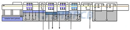
Inline systems are a cost-effective and time-saving solution for cleaning electronic components for large production and minimal component diversity. The PCB automatically runs each process step on the conveyor belt. In separate chambers, we usually clean, rinse and dry.
When we decide on the inline process, we prioritize footprints. Compared with the batch cleaning machine, this machine needs more floor space. We can integrate this system into the production line and put it into use after the entry and exit of components and the cleaning itself are completely automated.
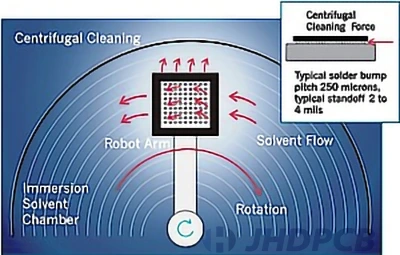
Inline Mechanism

Because the desired process is confined to one chamber, the system occupies a small area. It includes cleaning, rinsing and drying. The system is determined by the direction of the force acting on the pollutant to be removed, which makes the product rotate in the center of the treatment room to remove the pollutant calmly.
We will dissolve the particles on the surface of the product by immersing the product in the cleaning solution, and then use gravity to wash away the stubborn stains from the interception space by rotating. In order to avoid any redeposition, we usually distribute the rinsing solution (usually deionized water) to the spinning product after soaking and drain it immediately. After the continuous rotation of the product is completed, the drying cycle simultaneously introduces the filtered hot air into the process room.

Centrifugal Cleaning

What are the technical difficulties and roles of BGA inspection?

As we all know, BGA inspection is very difficult, one of the reasons is that the solder joint is located under the BGA package. Due to the positioning of this function, it may be a challenge to obtain a good view of the BGA for inspection. Despite this difficulty, inspection is crucial for BGA for several reasons:

  • Welding difficulty: it is very difficult to weld BGA components, because it needs to apply enough heat to the array so that all the balls in the grid can melt sufficiently to form solder joints. Both the connection density and the welding difficulty mean that the possibility of defects is high. The best way to help experts find these defects and avoid sending out faulty parts is to check them.
  • Unreliable electrical test: in order to ensure good electrical performance, we usually use electrical test to run current through PCB. However, this test can only judge whether the current is on or not when the BGA module is connected. These tests are unreliable because they can only find a few types of defects and can’t find the exact location of any defects found. Only by combining this method with other technologies can we find out the errors and their locations more completely.
  • Recycling of materials: if we find defects in the welding of BGA electronic boards, we can send them to the rework station, remove them, update or renovate them, and then recycle them. Finding defects in electronic boards during early inspection is also a way to save materials and reduce material waste.
  • Quality control: In order to reduce bga package costs, quality control technology is also one of the means we use. This check can also identify common defects and patterns. Quality control technology includes two categories: sampling inspection and process quality control. The latter is our common method in the bga assembly process. It refers to the inspection of random samples of products in the production process to determine whether the process is produced within the predetermined mark. Then we make corresponding adjustments according to the situation.
  • Cost reduction: In order to reduce costs, we need to minimize the number of defects transferred to the next production stage through comprehensive testing. If further defects are found during inspection, we need to rework. Once reworked, the cost will increase. Therefore, the earlier defects are found, the lower the cost will be. This is the key to reducing costs. Therefore, we need to find all problems and find out their location and causes before they become larger and more expensive.

What are the Common Types of BGA Tests?

In order to avoid defects and reduce production costs, we always need to analyze whether the connection between BGA package and PCB is defective by checking BGA. Because there is no way for us to directly identify problems with such a delicate product as electronic board, we need to use various inspection techniques and tools to find defects. The commonly used inspection techniques and tools are as follows:

Electrical test is to determine whether there are quality problems in installation or manufacturing of electrical systems and equipment before they are put into use, so as to determine whether newly installed or operating electrical equipment can be put into normal operation. The insulation performance, electrical characteristics and mechanical properties of individual electrical equipment in the electrical system shall be tested and verified item by item according to relevant provisions in standards, procedures and specifications. Through these tests and verifications, the defects, errors and quality problems of electrical equipment during manufacturing and installation can be found and eliminated in time to ensure that the electrical system and electrical equipment can be put into normal operation.

Visual inspection refers to a kind of inspection method in which inspectors observe or measure the surface of industrial products with the aid of optical instruments under the condition of visual inspection. It is usually used to detect incomplete penetration, spatter, undercut, pit, inclusion, air hole, crack, delamination, corrosion, erosion, size measurement and other problems on the surface of workpieces such as welds and castings.

X-ray testing is the most advanced testing method of BGA. It uses X-ray technology to observe, study and inspect the microstructure, chemical composition and other test technologies of materials to check whether there is a que in the electronic version. Such as X-ray powder diffraction, X-ray fluorescence spectroscopy, X-ray radiography, X-ray topography, etc. The X-ray tube emits more X-ray through the circuit board, and gathers them in dense areas such as solder joints. Then, the detector converts them into visible light and generates images. Through analysis and observation from different angles, similar defects such as solder bridge, popcorn and excessive solder can be identified. However, this technique is not good at detecting open circuits.
Both the endoscopes and X-ray inspection technology can also be used for various applications other than BGA inspection. Some examples include through-hole and Through-Hole Assembly detection, surface mount defect analysis, and lead-free solder detection.

What are the Common BGA package Defects?

Due to the complexity of BGA, it was many potential defects that may occur in the welding process of BGA. These problems include the following:

  • Misalignment: Misalignment is one of the most common problems during BGA assembly. It usually occurs when PCB and BGA are offset during reflow soldering and the connection point is incorrect.
  • Inconsistent standoff height: Inconsistent standoff height will endanger the safety of connection. The BGA setting on the PCB surface is skewed because it is caused by improper welding when the BGA is set on the top of the PCB.
  • Ball leakage: During the assembly process of connecting BGA to PCB, the ball leakage is the most likely error, which may be due to the lack of necessary connection points during the assembly process.As a reliable china pcb assembly bga factory, we strictly control the assembly soldering process. Avoid ball leakage events.
  • Non wetting Pads: Due to incomplete reflow or residual solder resist in previous steps during production, reflow paste may not wet pads correctly in some cases.
  • Bridging: Bridging is a kind of PCB welding problem. It refers to the phenomenon that too much solder leads to PCB pads connected together. Bridging is not easy to find, but it can cause fatal damage to PCB.
  • Partial reflow: Partial reflow is usually caused by insufficient reflow soldering, human error or mechanical failure, which means that the current only partially covers the circuit board.
  • Popcorn: Popcorn phenomenon refers to the phenomenon that the moisture existing in an integrated circuit or SMD in the device is heated rapidly during the repair process, which causes the moisture to expand, causing micro cracking or cracking. This is a common problem of BGA, which also leads to short circuit.
  • Open circuit: Open circuit refers to the circuit state when there is no current between two points in the circuit or the conductor with very large impedance value (or resistance value) is connected. Even though the electrical test can identify the problem, the cause cannot be determined.
  • Voids: In collapsible BGA components,voids are the most common problem . This is caused when there is no welded connection where the flow stops.

The fatal errors of the final product may be these problems, so we must find these errors by using quality inspection techniques and techniques. Fortunately, with the development of modern detection technology, we can already use one or more detection methods to identify the extent of most defects. However, it is important to avoid these defects before assembly as far as possible.

Application of BGA Assembly Technology.

Since BGA allows the use of IC device packages with hundreds of pins (high density miniature processing chips). Integrate more functions in a smaller space, so BGA packages are often used in high-density PCB products. At the same time, the good solderability, electrical performance and heat dissipation of the BGA package are also excellent. The advantages of various aspects make it widely used, such as:

  • Notebook computers,
  • Intelligent mechanical equipment,
  • Intelligent robots,
  • IoT smart home,
  • Medical equipment,
  • Military equipment,
  • LED industry,
  • Radio communication,
  • Aerospace,
  • Satellite fields.

JHDPCB's BGA Assembly Capability.

BGA Assembly Capability of JHDPCB-
JHDPCB has many professional engineers and high-end machines. While providing high quality, we also provide high-precision BGA packaging technology. Turnkey services for BGA assembly and other assembly methods are also available.BGA assembly quotes in shortest time and we will provide you with the most reasonable bga package price.

Our advanced SMT assembly equipment-
We have a full-automatic SMT production line to ensure high precision and high yield of assembly. Our latest equipment includes automatic soldering machine, automatic mounter, reflow furnace, X-ray, etc. to create better product services.

Our BGA Checking Flow-
Solder quality inspection for BGA packages is complicated by the fact that the solder balls are located under the die. Traditional optical methods cannot tell if a solder joint has inspection or voids. We can improve the detection accuracy by using the combined detection method of electrical measurement, boundary scanning and automatic X-ray detection. The premise is that there are BGA components in the SMT assembly produced by the smt bga assembly factories.

Our BGA Assembly Capabilities-
Because it requires precise control, ball grid array welding is traditionally accomplished through an automated process. JHDPCB can create high-quality and reasonable-yield BGA assembly PCBs for you. The BGA of the minimum spacing size that we can assemble is 0.25mm. We provide the following types of BGA assembly services: PBGA (Plastic Ball Grid Array), CBGA (Cellular Ball Grid Array), TBGA (Tape Ball Grid Array), EBGA (Enhanced Ball Grid Array), FC-BGA (Flip Chip Ball Grid Array), MBGA (Metal Ball Grid Array), Micro BGA, MAPBGA and TEPBGA, etc.

Nowadays, most manufacturers have mastered BGA assembly technology. As a PCB manufacturer with many years of experience, JHDPCB provides BGA components that are higher than the industry standard and undergo strict factory inspection. It is recommended to have BGA assembly for your PCB by an expert, JHDPCB must be your best choice. If you need more information about PCB packaging or have any questions, please feel free to contact us. JHD’s professional customer service team will provide the best advice for your PCB production and assembly.