automatic optical inspection

Automatic Optical Inspection (AOI) Guidelines in PCB Manufacturing

directory

What is automatic optical inspection?

The typical AOI setup consists of many HD, HDR, and magnification cameras, a powerful light source, a central processing and memory device, and an operator. Printed circuit board assemblies are typically tested for flaws using the automated visual inspection technique known as AOI (PCB assembly). To guarantee that the goods leaving the production line are of the highest quality, that they are constructed correctly, and that they are free of manufacturing flaws, AOI can swiftly and precisely inspect electronic assemblies, notably PCBs.

PCBAs are automatically scanned by AOI using cameras to look for two different sorts of failures:

  • Catastrophic failures, such missing parts…
  • Quality failures, including crooked parts or malformed fillets.

It is crucial to perform AOI at various phases of the PCB manufacturing process since components are now typically spread densely over the board, which results from the fact that PCBs typically start with 4 layers. Both bare PCBs and PCBs filled with electrical components can undergo AOI.
AOI is crucial to ensuring that the PCB meets quality standards and that faults, failures, and any irregularities may be found early on, allowing the process to be paused, the failure to be fixed, and then the process to resume. As a result, there are fewer cases of too many PCBs failing at the conclusion of the process. This guarantees fewer fake PCBs, which lowers overall PCB production costs. Uniquely, AOI is carried out following reflow soldering to find solder junction flaws early in the manufacturing process.

Importance of automated optical inspection test.

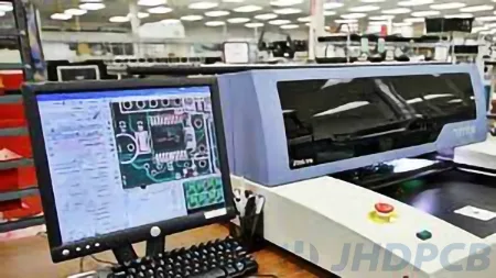
Your product will function properly if your PCB design is accurate and you have assembled the right parts in the right places. It will concentrate on identifying and fixing any manufacturing flaws or manufacturing defect analysis during production. AOI is crucial to the creation of PCBs. Every board has great performance that is guaranteed by this, making it suitable for demanding electrical applications. When AOI discovers a PCB flaw, it flags the board for repair and return. There are numerous methods in which this process can take place. A facility’s unique needs, such as the need for all traces on a circuit board to be larger than a certain size, might not be met by an AOI’s findings. In this situation, a person can examine the results and decide which boards need to be sent back for more work. Alternately, AOI can contrast a real PCB with a CAD rendering of an ideal PCB. When a board deviates from the ideal design, AOI can automatically spot it and flag it for rework.

The following advantages of AOI are available for PCB manufacturing:

  • Ensure Quality: AOI enables you to guarantee the performance of your PCB product. Assuring product quality can help you boost customer happiness, improve your company’s reputation, and feel confident in the worth of the services you offer your clients.
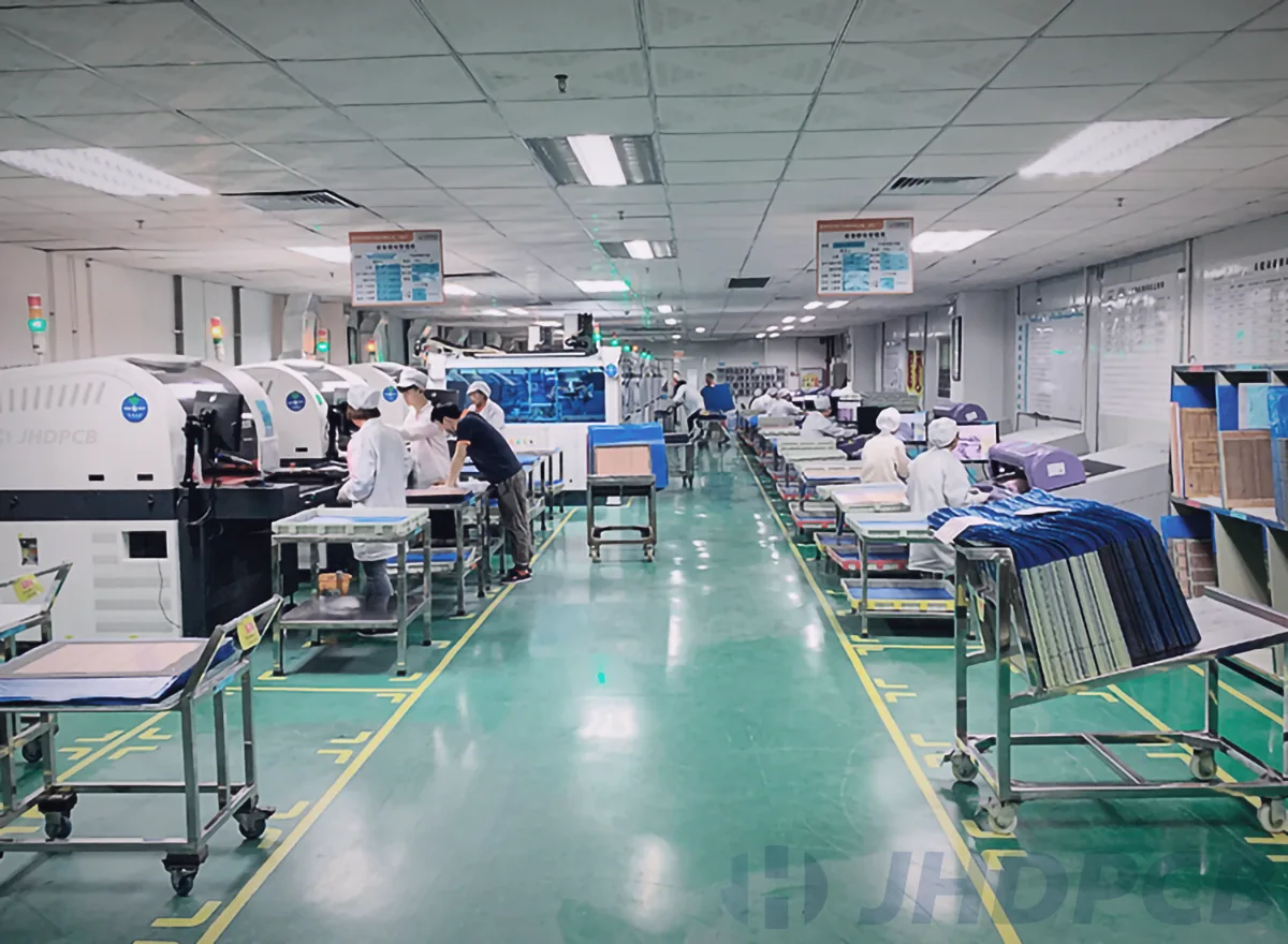
  • Analyze intricate boards: At Millennium Circuits, AOI is automatically performed on any of our boards that have more than 100 components. Complex circuit board designs can be examined by AOI with a level of accuracy unsurpassed by the human eye.
  • Process Improvement: If a defect is brought on by a flawed process, promptly capturing the defect with AOI can assist you in identifying defect patterns and modifying your process before you produce thousands of boards with the same failure. According to a recent study in the International Journal of Engineering and Applied Technology, it only costs 10 times more to detect a flaw on a freshly constructed circuit board than it does on a bare board. Circuit board defect finding is 1,000 times more expensive to utilize. Early error detection reduces the possibility of future rework and improves the effectiveness of your production processes.
    The AOI process is automated, however operators can set settings to instruct the scanner what to look for. It is simple to update your parameters to locate the needed flaws if your design specifications change.
  • Decreased damage: It is easier and more cost-effective to prevent repeating the same issue on a bigger scale the earlier a manufacturing process failure is identified.

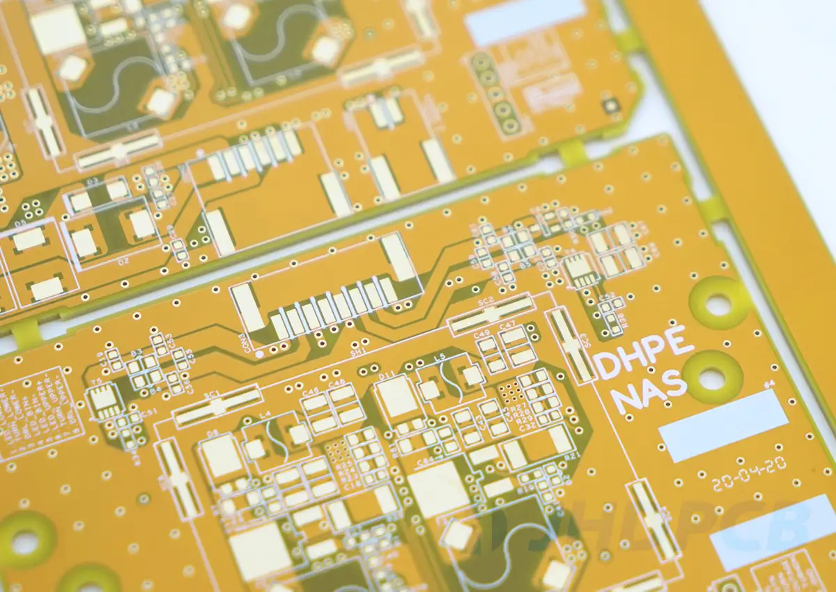
Your PCB board is a crucial component in electrical devices and plays a significant function in many ways. Being the brain of your product, it must be designed with extreme precision and strictness. Moreover, printed circuit boards will advance in complexity even as they get smaller. It is possible for even very simple boards to have thousands of solder joints, making human inspection difficult or impossible. In conclusion, in the PCB manufacturing industry, AOI is a must.

AOI test

Features of automatic optical inspection.

Advantages of AOI for PCB Inspection:

By now, we are aware of the advantages of PCB AOI testing thanks to the aforementioned hints. The following are some advantages:

  • Detection of Visual Defects:The board’s surface imperfections, such as stains, missing or improperly placed components, soldering errors, and scratches, can be precisely found using AOI. Any of these evident flaws can be readily missed by human sight since they are so little.
  • Flexibility:The nicest thing about AOI is that it may be used at any point in the process and that it can be repeated if necessary.
  • Detection of Defects in PCB Assemblies:AOIs may precisely identify faults in PCB assemblies as well as individual PCBs. Inspection of PCB assembly comprises, among other things, locating flaws in values, polarity, and component soldering.
  • Cost Effectiveness: When compared to a few other inspection techniques, such as X-ray inspection, AOI is more affordable. Moreover, AOI saves the PCB manufacturer money over time by reducing the likelihood that errors will be repeated and by raising manufacturing quality.
  • Reliability: Without a doubt, AOI is a very trustworthy procedure that produces accurate results.

Disadvantages of AOI for PCB Inspection:

  • Maintenance costs: Particularly for small-scale or low-volume production, automatic optical inspection system systems can be expensive to buy, install, and maintain.
  • Limited detection capabilities:AOI systems sometimes struggle to find faults like microcracks or those that are concealed on the Board.
  • Complexity: For AOI systems to function properly, trained operators and technical assistance are needed.
  • Adaptability:AOI systems may not be able to adapt changing inspection requirements or new items without significant modifications because they are optimized for particular types of inspection.

How does AOI work?

AOI inspection is an inspection that inspects and tests circuit boards for any possible defects. AOI test pcb uses automated machines to test PCBs. This PCB inspection technique checks for errors such as component placement defects.

The PCB board’s surface is scanned during the AOI examination. The HD color cameras on the AOI machine scan the surface at high magnification, clearly displaying on a larger monitor the intricacies of each PCB piece and each component within it. The camera uses a light source, such as fluorescent or LED lights, PCBs, UV or infrared light, to take pictures of the PCB surface.
After that, the image is compared to the pre-programmed information and supplied into the AOI processing system’s memory. The process is instantly stopped if the difference or Normalized Cross Correlation (NCC) is determined to be greater than the tolerance level. The difference between captured and pre-programmed (template) photos decreases with increasing NCC. Several algorithms running on the AOI machine dependent on pixel counts and NCC values determine the ultimate decision to deem the board to be defective and thus stop the process.

The AOI machine operator can manually halt the process as needed by visually inspecting the images the AOI machine has captured on the screen. By separating the object image from the backdrop, the “blobs or pixels” of the pixels-based image are integrated or grouped, and errors are then found.
To check for component placement, location, and condition (i.e., flaws unrelated to soldering), the AOI can be performed prior to reflow. The post-reflow AOI finds flaws that may have resulted from the reflow oven’s thermal dynamics in soldering joints, components, and the PCB board itself.
Smallest components like 01005, 0201, and 0402 packages as well as IC packages like QFP, QFN, CSP, and BGA and PoP can be scanned by the AOI machine, but only for surface inspection, not for underneath the package examination. It should be noted that AOI cannot inspect components that are located under the body or packaging of an IC.
AXI is required for this. As X-Rays can see through the body, the component identification underneath the IC package can be done using greyscale pictures.

What type of lighting system is used for automated optical inspection?

A crucial component of the AOI system is lighting. It is easier to emphasize various types of defects by using the right lighting source. The ability to employ lighting to enhance the photos that are available has been made possible because to recent advancements in lighting technology. This makes it easier to highlight flaws, which reduces the amount of processing needed while increasing speed and accuracy.

Most AOI systems feature a set of predetermined illumination. This will depend on the procedure needed and the kinds of products that need to be evaluated. Often, these have been adjusted for the predicted circumstances. Yet occasionally, some personalization may be necessary, and knowledge of lighting is usually helpful.
A variety of types of lighting are available:

  • Fluorescent lighting: As fluorescent illumination provides an efficient method of lighting for seeing faults on PCBs, it is frequently utilized for AOI, automated optical inspection applications. For AOI applications, the fundamental issue with fluorescent lighting is that the lights deteriorate over time. As a result, the automated optical inspection system will be exposed to lighting that is continually changing in both intensity and quality.
  • LED lighting: Automated optical inspection systems (AOI) are now able to use a lighting source that is much more stable because to the advent of LED illumination. Although the light output from the LEDs does decrease over time in LED lighting, this may be overcome by raising the current. The amount of lighting can also be managed with LED lighting. So, compared to fluorescent or incandescent lights that were once popular, LEDs provide lighting that is much more effective and efficient.
  • Infra-red or ultra-violet: In some cases, infrared or ultraviolet lighting may be needed to highlight specific flaws or to enable automated optical inspection to detect particular flaw types.

For an autonomous optical inspection system, or AOI, the positioning of the lights is just as crucial as its design. Positioning the light sources is necessary not only to ensure that all regions are effectively lit, which is crucial because some components could cast shadows, but also to draw attention to flaws. Many assembly can require careful adjusting. It is worth noting that: LED PCB manufacturing has always been our strength, and JHD has provided perfect solutions for many industrial machinery, education and indoor and outdoor lighting customers.

What are the types of failures detected by AOI?

Detectable bare board failures:

  • Surface defects such as nodules and scratches,
  • Dimensional defects such as openings and shorts, thin solder,
  • As well as incorrect, missing and misaligned components.

For PCBs with components (SMT inspection):

  • Insufficient solder joints,
    solder bridges,
  • Excessive solder joints,
  • Billboards,
  • Tombstones,
  • Solder balls,
  • Package height (3D AOI),
  • Coplanarity (3D AOI),
  • Component polarity,
  • Component presence or absence,
  • Component flips,
  • Improperly placed or misaligned components,
  • Area defects, volume defects, height defects,
  • Shorts,
  • Line width infractions,
  • Spacing infractions,
  • Excessive copper pads,
  • Cuts,
  • Damaged holes (whether a via extends beyond its pad).
  • Incorrect component values,
  • Fake parts,
  • BGA package shorts and opens,
  • Poor solder quality.

Processing system for AOl.

Automatic optical inspection, or AOI, requires that the specifications for an approved board be recorded within the system before it can evaluate a PCB assembly. If the AOI system is to correctly detect any faults on the PCB assemblies passing through, this programming task must be done appropriately.
Programming an AOI system can be done in a number of ways:

  • “Golden Board” usage: One approach is to give the AOI, automated optical inspection system, a known-good board to serve as a target. The system receives this so that it can pick up on the pertinent attributes. In addition to many other things, it will examine the parts and the solder profiles of each junction. Many boards are frequently needed to give the system with enough variance data.
  • Programming using an algorithm: After receiving PCB data, the system creates its own board profile. Real boards will be needed for this plan as well, although they will be needed less frequently.
    Both methods have pros and downsides. Setup time, upkeep, accuracy, and the needs of the specific AOI, automated optical inspection system, must all be balanced. Usually, the needs will be greatly influenced by the machine being used.

Any facility that produces printed circuit boards must have the ability to inspect the quality of the boards as they leave the production line. Only in this way are they able to keep an eye on quality and, when issues are found, correct the procedure to prevent similar issues from affecting subsequent boards. So, two crucial instruments for the manufacturing sector include automatic optical inspection and, when necessary, X-ray inspection.

Validate other inspection techniques for PCBs.

Manufacturers must check that all components are assembled properly for a PCB to work as intended. This is accomplished using a variety of ways, from straightforward human examination to automated testing employing cutting-edge PCB inspection tools.
A manual visual inspection is a good place to start. For relatively simple PCBs, they may be all that is needed.

ICT is mostly utilized for PCBA electrical testing (Printed Circuit Board Assembly). Essentially, it can be compared to an advanced [LCR meter] or “multimeter.” Electronic components do not need to be removed from After the circuit board has been removed, the pin point can be used to determine the electrical characteristics of every component on the board and whether there is a short circuit or open circuit issue.

A new class of test technology called AXI has only recently come into existence. An X-Ray emission tube is located above the assembled circuit board (PCBA) when it enters the machine along the guide rail. The X-rays it emits pass through the PCBA and are received below the detector, which is typically a camera. Because the solder joints contain lead, which can absorb a lot of X-rays in comparison to other materials like glass fiber, copper, silicon, etc., the X-rays irradiated on the PCBA are more concentrated. Simple image analysis methods may automatically and reliably identify solder joint flaws because the dots generate high-quality images that make the examination of solder joints fairly simple.

PCBs have grown more and more complicated as a result of the development of surface mount technology. Boards are increasingly more compact and contain smaller components as well as chip packages like BGAs and chip-scale packages (CSPs), which conceal hidden solder connections. For visual inspections like MVI and AOI, these capabilities provide difficulties. Combined with flying probe testing, a more detailed inspection of the PCB can be performed.

Equipment at a manufacturing plant and hardware equipment are frequently subjected to burn-in testing. Before a product is made available to the public or sent to consumers, they might find any problems.
Burn-in testing may be carried out on the overall system or on a modular level on each individual component. Burn-in testing is likely to reveal any problematic components, if any. Burn-in testing is typically used to establish the highest temperature that electronic equipment can endure.

AOI, AXI, ICT main defect detection capability comparison
Defect type AOI AXI ICT
Open circuits Y Y Y
Solder bridges Y Y Y
Solder shorts Y Y N
Insufficient solder N Y N
Solder void Y Y N
Excess solder N Y N
Solder quality N Y N
Lifted lead Y Y Y
Missing component Y Y Y
Misaligned or misplaced component Y Y Y
Incorrect component value N N Y
Faulty component N N Y
BGA shorts N Y Y
BGA open circuit connections N Y Y

AOI image acquisition and analysis.

The image acquisition system is one of the most important components of an AOI automated optical inspection system. This records a picture of the PCB assembly, or printed circuit board, which is later examined by processing software within the AOI system. Depending on the individual application and the complexity/price of the AOI system, there are numerous versions of image capture systems.
A single camera may be used in imaging systems, while numerous cameras may be used to enable improved imaging and 3D capabilities. Also, the camera ought to be able to move with the aid of software. This will make it possible to relocate them to the ideal spot for a specific PCB construction.
Beyond that, performance can also be impacted by the kind of camera. The choice of camera depends on the balance to be struck between speed and accuracy:

A whole frame of streaming video is taken from an automated optical inspection, or AOI, camera. Signal processing can then be done on a still image created from the collected frames. Although this technology is relatively quick, it is not as accurate as other still picture methods.
System for still-image cameras: usually situated close to the target PCB, necessitating the need of an effective lighting system. It can also be important to have software that can shift the camera.
An AOI system inspects a board picture for a number of distinct characteristics, including component positioning, component size, board fiducials, label graphics (like barcodes), backdrop color, reflectivity, and more. The AOI system additionally inspects welded joints as a crucial component of its purpose to make sure they demonstrate that the joints are satisfactory.

Board differences must be taken into account by AOI systems while studying boards. Components differ significantly between batches not just in terms of size but also in terms of color and reflectivity. While silkscreen printing, ink thickness and color typefaces might occasionally differ slightly.

AOI inspection of JHDPCB.

Smart features to automate your inspections.
Wafer flaws and interesting features can be found using an AI analyzer trained on sparse data. The analyzer can be incorporated into production tools after training and start automatically identifying and categorizing faults. Its automation eliminates the possibility of operator error while producing extremely repeatable inspection findings.
A program developed by JHDpcb compares non-defective die to other dies and gives the position coordinates of every defective die, regardless of whether they are systematic flaws brought on by the photomask and exposure process conditions group or random faults brought on by particles. After that, the automated system creates a defect map report listing all flaws found on the wafer.

Solve your detection challenges with custom innovations.
Every problem that one of our clients faces offers Nanotronics a chance to innovate. With specialized software and hardware, we help our customers overcome obstacles in a variety of industries, including semiconductors, aircraft, automotive, medicines, and advanced materials.
To understand the benefits of a fully tested and inspected PCB, please work with JHDpcb. We offer a wide variety of different boards, from aluminum PCBs to high current and heavy copper PCBs to specialty boards, so you are sure to get the right PCB for your industry and application. Please contact us for one-stop PCB production and thorough inspection.

Get a PCB Quote Now

Open high-quality PCB manufacturing services in JHDPCB

Leave a Comment