The Ultimate Guide to Flying Probe Testing (FPT) of PCBs

jhdpcb@gmail.com
In the world of PCB manufacturing, ensuring the functionality and reliability of electronic devices is paramount. To achieve this, robust testing methodologies are essential. Flying Probe Test (FPT) has emerged as an advanced technology that addresses the challenges posed by complex PCB designs and tight production schedules. At JHDPCB, we specialize in Flying Probe Testing, offering our clients high-quality PCBs that undergo thorough and efficient testing.
The Flying Probe Test revolutionizes traditional testing approaches by replacing the need for bed-of-nails fixtures with automated probing systems. These systems employ moveable probes that can quickly and accurately access test points on the PCB without requiring dedicated fixtures. This non-contact probing method enables comprehensive testing of complex boards, including multilayer and densely populated designs, while minimizing setup time and costs.
At JHDPCB, we recognize the critical importance of Flying Probe Testing in ensuring the functionality and quality of our PCBs. With our state-of-the-art facilities and advanced testing equipment, our skilled technicians meticulously analyze every aspect of the PCB’s electrical connectivity, component placement, and signal integrity. Our Flying Probe Testing process detects faults such as open circuits, short circuits, and component placement errors, providing invaluable insights to optimize the manufacturing process and deliver reliable products to our clients.
In this article, we will explore the world of Flying Probe Testing, examining its advantages, working principles, and its role in ensuring the quality of PCBs. We will showcase JHDPCB’s expertise in incorporating Flying Probe Testing into our PCB manufacturing process, highlighting our commitment to delivering reliable, high-performance PCB solutions.
Join us as we embark on an informative journey through the intricacies of Flying Probe Testing, uncovering the immense value it brings to the PCB manufacturing industry, and how JHDPCB’s capabilities set us apart in providing top-notch PCB testing services.
What is the Flying Probe Test (FPT)?
The Flying Probe Test (FPT) is a is a technique that is both highly efficient and cost-effective in detecting defects and faults in printed circuit boards (PCBs). Unlike traditional testing methods that require custom fixtures or tooling, the FPT machine uses movable probes to test the electrical connections on the PCB without any physical contact. This makes it ideal for testing complex and densely populated boards.
Originally used only for bare-board testing, FPTs have evolved to measure not just resistance but also capacitance and inductance. This has made them beneficial for use on PCB assemblies as well. They are more cost-effective for smaller lots of production and offer improved test coverage over traditional ICT testing. By employing automated probing, FPTs can directly access component pins, thus eliminating the requirement for specially constructed test points. As a result, FPTs have emerged as a favored and cost-effective approach for testing low-volume and prototype circuit boards.
FPTs have become a preferred and cost-effective method for testing low-volume and prototype circuit boards. They are easy to program and use even for very dense and complex boards and can decrease the product design cycle and reduce time to market. Furthermore, significant advancements are underway in FPT technology aimed at enhancing the test coverage percentage, which in turn leads to improved quality and reduced testing time.
With a camera to inspect component polarity and the ongoing trend of miniaturization in electronics, FPTs have great potential to become even more attractive for testing, especially for smaller size electronic gadgets where board real estate is a precious commodity. Overall, the Flying Probe Test is an efficient and versatile method for testing PCBs that has become increasingly popular in the electronics industry.
Basic Guidelines for Test Point Design.
By following these guidelines, designers can ensure the effective use of the FPT process in testing printed circuit boards. These guidelines for test point design ensure the effective use of the Flying Probe Test (FPT) process:
- Accessibility to Nets
Nets linked to the active components must be accessible on the same side of the test probes to enable the “open fix” option. This rule applies to SMD components as well. A distance of 2.8 mm must be maintained between the probe and the probe sensor for better efficacy. However, this condition does not apply to the vertical testing procedure and to the board that is to be tested on both sides. - Features of Test Points
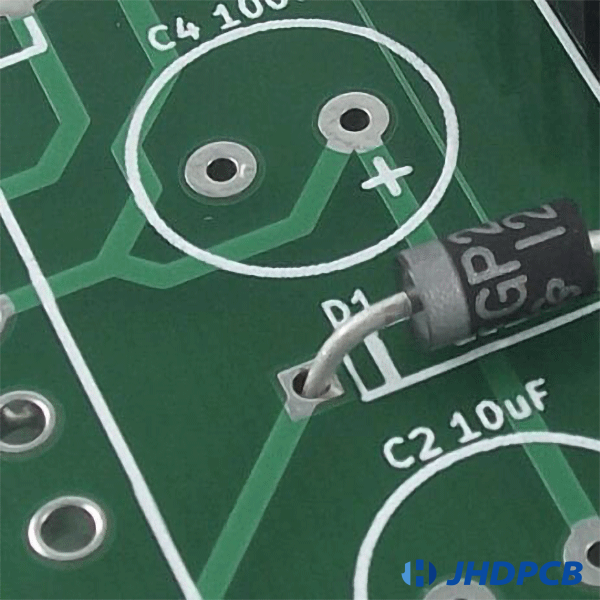
Test pads without solder resist, vias, through-holes, plated-through holes (PTH), and surface-mount device (SMD) component pads are the preferred contact points for the FPT process. Also, the size of a test point depends on the probe type, with a minimum size of 6 mils (20 mils recommended). For optimal results, the spacing between individual test points should be a minimum of 10 mils and preferably 20 mils. - Vias
The diameter of vias should be between 8 to 20 mils (10 mils recommended). Also, they must be occluded and free from the solder resist. When dealing with SMD components, especially those with step sizes slower than 25 mils, it is advisable to use longer solder pads than the component pins to ensure that the testing probe can make contact with the test point on the soldering pad itself. For horizontal architecture (PILOT L4/H4), components should be 4 to 5 cm higher than the opposite of the test side. - Board Clamping
The board should be secured with a clamp or conveyed via horizontally (Pilot L4) or vertically (Pilot V8). For testers with horizontal architecture, provide support after every 150 mm or the distance based on your design requirement on both axes (except the Aerial and V8 test systems) to keep the board flat. - Board Dimensions
The maximum board dimensions are 600 x 1010 mm for Pilot L4 testers and 600 x 540 mm for Pilot V8 testers. Also, the CAD data must include the component height. - Test Point Distances
The clearance is the distance between the center of the test point and the side of the components. Moreover, the minimum distance between a test point and the component can be estimated by the formula: L = (0.29 x Height) + 0.7 (in mm). - Fiducial Recognition
Include three fiducials for each board and position them in a triangle shape on either side of the board. Different arrangements of the fiducials should be achieved to eliminate side errors. For larger boards with dimensions greater than 400 mm, place local fiducials concerning the fine-pitch components that must be visible after the component has been mounted. - Wire Connection
Wiring should be refrained from colliding with the test points.
How Does a Flying Probe Tester Work?
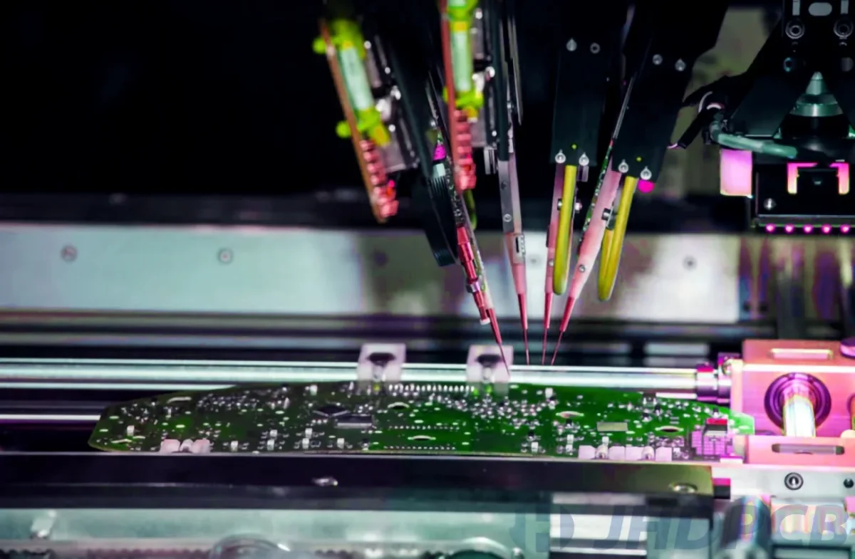
Flying probe testing is a powerful testing method for printed circuit board assemblies (PCBAs) that offers flexibility, accuracy, and cost-effectiveness. The process of creating an FPT test program begins with the use of an FPT test program generating application, which requires the PCBA’s bill of materials (BOM) and the ECAD file. To perform FPT, an intelligent CAD file in ODB++ format, IPC-2581 format, or native ECAD design file format (rather than just Gerber) is required, along with an Excel format BOM. Once the test program is generated, it is loaded into the FPT tester.
The PCBA to be tested is then placed on a conveyor belt, which moves into the tester area where the probes are located. During the test program, the probes make contact with the pads (both component and test pads, if any) and unmasked vias, as per the already loaded test program. The tester applies electrical test signals and power to the probe points and makes measurements to determine if the circuit portion within the probes is giving the expected results within specified tolerances. In this way, FPT detects defects in the unit.
FPT hardware is equipped with signal generators, DC and AC power supplies, various types of sensors, a multiplexing system, digital multimeters, frequency counters, etc., which are used to provide signals to excite the PCB nodes and to make measurements on the nodes of the components and interconnections on the PCBA. To isolate component segments between the testing probes from the rest of the interconnections to other components on the board, FPT uses a complex scheme of excitation signals.
This “virtual isolation” of components from the rest of the circuit interconnections makes it possible to measure component values as accurately as possible, while they remain connected in the circuitry on the board. FPT can test for shorts, opens, and component values. It is also equipped with a camera to help automatically inspect component polarity and performs “diode” impedance tests on inputs of integrated devices whose functional behavior is outside the scope of testing of the FPT.
Additionally, many FPTs available today can excite with signals and make some measurements on the pads of the ICs that are underneath their bodies (such as BGAs, QFNs, and other leadless devices) by capacitive probing. So that was all the basics of how flying probe tests work, now let’s take a look at some advanced features of testing through probes:
- Phase Difference Measurement Unit
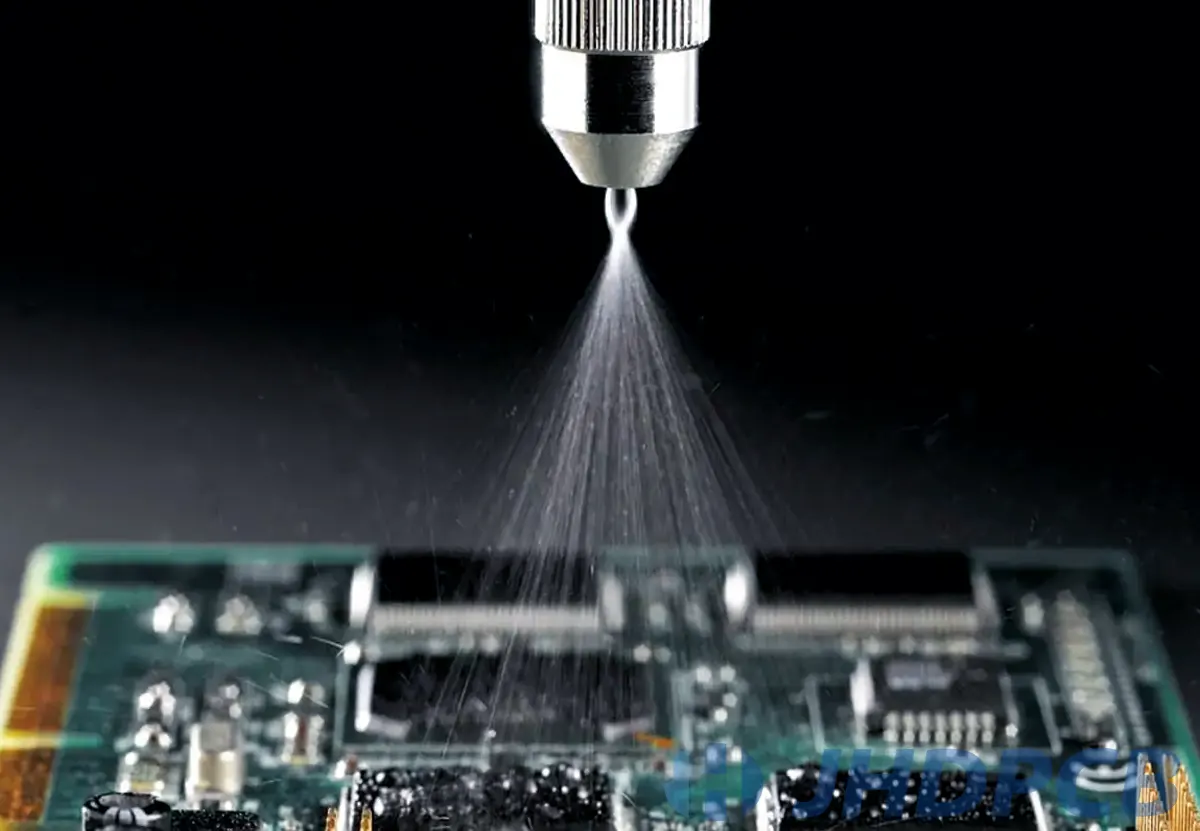
The PDM (Phase Difference Measurement Unit) is an advanced feature that allows for the measurement of the phase difference between the reference and signal line sections by sending a high-frequency signal between one endpoint of each. This eliminates the need for isolation tests within a net, making it a valuable tool for circuit testing. - High Voltage Stress Test (HVS)
The High Voltage Stress Test (HVS) is a testing procedure designed to identify high-resistance isolation defects that may be undetected by PDM. HVS achieves this by applying high voltage pulses between signal lines, allowing it to detect high-resistance defects. Like PDM, HVS inspects each net once, making it a fast-testing method. HVS also offers the option of applying higher voltages of about 500V to 1000V, which exceeds the maximum voltage applicable in standard isolation resistance measurement (typically 250V). However, HVS uses a low-power test to ensure that the super high resistance test is conducted without adding undue stress to the tested boards. - Micro Shorts Detection
It is another advanced feature that can avoid damage and trouble caused by the sudden application of high voltage during isolation tests. This feature applies low voltage initially and then gradually increases the voltage to detect micro shorts. In some cases, high-resistance shorts between multiple layers of a board can exhibit characteristics similar to semiconductors and capacitors. Additionally, reversing the polarity of the high voltage can also help detect such defects. FPT is a comprehensive testing method that aims to test the board as thoroughly as possible, while taking into account the accessibility constraints posed by a particular board design. JHDPCB is a reliable provider of high-quality PCBs and offers testing services such as FPT to meet your PCB manufacturing needs.
Features of Flying Probe Test.
While the Flying Probe Test has several advantages that make it a popular choice for testing electronic components, it also has some limitations that need to be considered carefully before choosing this testing method. Let’s discuss some advantages and disadvantages of flying probe tests.
Advantages:
- Non-destructive: A key benefit of the Flying Probe Test is that it is a non-destructive testing technique. This means that it can test electronic components without damaging them. It is particularly useful for testing high-value or delicate components that cannot be replaced easily.
- High accuracy: The precision of the probes used in the Flying Probe Test allows for highly accurate measurements and testing. This enables it to detect even the most minor faults in electronic components.
- Versatile:Flying Probe Test is a versatile testing method that can be used for a wide range of applications. It can be used for testing bare boards, assembled boards, and complex circuits.
- Flexible:Flying Probe Test is a flexible testing method that can test both sides of a board and can be easily reprogrammed for different testing requirements. Flying probe test point requirements makes it highly suitable for testing complex circuits with multiple layers.
- Component orientation and alignment testing:FPT can circuit check electronic component polarity, orientation, and misalignment, ensuring that all components are installed correctly.
- Rapid feedback:The setup test time for Flying Probe Test is relatively quick, as compared to other testing methods. This is because it does not necessitate expensive fixtures or tooling, which can save both time and money.
- Cost-effective: Flying Probe Test can be a cost-effective solution for low to medium-volume production runs. It is because it does not require expensive fixtures or tooling, which can help reduce costs.
- FPGA verification:FPT provides the ability to do on-board verification of Field-Programmable Gate Arrays (FPGAs), which is a critical component of many modern electronic devices.
- Automated:Flying Probe Tests can be easily integrated into automated testing systems, allowing for high throughput and efficient testing. So, overall, it can help reduce labor costs and improve testing efficiency.
- Suitable for highly complex prototype PCB testing: FPT is highly suitable for testing highly complex prototype PCBs.
Disadvantages:
- Limited accessibility: Flying probe testing, like most other tests, does not power up the circuit, which means that it does not provide a complete real-world view of the product, unlike an ICT (in-circuit test). Also, FPT cannot test connectors and inactive components, which can limit its testing capability.
- Slow testing speed: Flying Probe tests can be slower than other testing methods, especially for large boards or complex circuits. In contrast to ICT, which uses fixtures to simultaneously insert probes into multiple points on a PCB for testing, FPT can test only one point at a time. This can lead to longer testing times and higher flying probe tester costs.
- Limited test coverage: Flying Probe Test may not be able to detect certain types of faults, such as intermittent faults, ball grid arrays, or problems that occur only under specific conditions. This can lead to some faults being missed during testing.
- Higher cost for high-volume production:For high-volume production runs, the cost of the Flying Probe Test can become higher than other testing methods due to the longer testing time. This can make it less cost-effective for large-scale production runs.
Which PCB Test Methods can be Combined with Flying Probe Test?
Flying probe testing services can be combined with several other PCB testing methods to improve test coverage, efficiency, and accuracy. Here are six PCB test methods that can be combined with flying probe testing:
Automated Optical Inspection (AOI):
AOI is a non-contact test method that uses high-resolution cameras and image processing software to inspect PCBs for manufacturing defects such as missing components, misaligned components, solder bridges, and other soldering issues. AOI is often used as a complementary test to flying probe testing, as it can detect visual defects that might be missed by electrical tests. Combining AOI with flying probe testing provides a comprehensive test strategy that addresses both electrical and visual aspects of PCB quality.
In-Circuit Test (ICT):
Ict-test is a powerful testing method that can detect a wide range of faults, including open circuits, short circuits, and component values that are outside of tolerance. However, ICT has some limitations.
To overcome these limitations, Flying Probe Test can be combined with ICT to provide more comprehensive testing of the PCB. A PCB flying probe test can access those points on PCBs which cannot be accessed by ICT fixtures, ensuring that all components are tested during the process.
This ensures that any faults in hard-to-reach areas of the PCB can be detected and corrected. By combining In-Circuit Test with Flying Probe Test, manufacturers can ensure that their PCBs are thoroughly tested and meet the required quality standards. This approach can provide a more comprehensive testing process, resulting in higher-quality products and fewer returns or failures.
X-ray Inspection:
X-ray inspection is another non-contact test method that uses X-ray imaging to inspect PCBs for hidden defects, such as solder joint voids, internal layer misalignment, and buried component issues. X-ray inspection can be combined with flying probe testing to provide a more in-depth analysis of PCB quality, particularly for high-density interconnect (HDI) boards or boards with hidden components like ball grid arrays (BGAs).
Boundary Scan (JTAG):
A boundary scan is an electrical test method that utilizes embedded test points and a standard Test Access Port (TAP) on the PCB to perform in-circuit testing. It is particularly useful for testing high-density PCBs, as it can test interconnects and components without requiring physical access to test points. Combining boundary scan with flying probe testing allows for increased test coverage, especially for boards with complex interconnects or limited test point access.
Functional Testing:
Functional testing refers to the process of evaluating a PCB’s functionality to ensure that it performs as intended in its ultimate application. This test method is usually performed using custom-designed test fixtures and software that simulate the PCB’s operating environment. Combining functional testing with flying probe testing helps to ensure that both the electrical and operational aspects of the PCB are tested thoroughly.
Thermal and Environmental Stress Testing:
These tests subject PCBs to various temperature and environmental conditions to evaluate their performance and reliability under extreme or varying conditions. Thermal cycling, temperature-humidity testing, and Highly Accelerated Life Testing (HALT) are some examples of these tests. Combining thermal and environmental stress testing with flying probe testing helps to identify potential weak points in the PCB design and electronics manufacturing process and ensures that the PCB will perform reliably in its intended application.
By adopting Flying Probe Testing, we at JHDPCB offer our clients a testing solution that combines accuracy, speed, and cost-effectiveness. Our state-of-the-art facilities and advanced testing equipment allow us to perform comprehensive analysis of PCBs, detecting potential faults such as open circuits, short circuits, and component placement errors. Through meticulous testing, we ensure that our clients receive PCBs that meet the highest standards of quality and performance.
Our dedication to excellence extends beyond our testing capabilities. At JHDPCB, we are committed to providing exceptional customer service, timely deliveries, and competitive pricing. Our skilled technicians and experienced team strive to meet and exceed the expectations of our clients, fostering long-term partnerships based on trust and satisfaction.
When it comes to PCB manufacturing, trust in the testing process is paramount. By choosing JHDPCB as your manufacturing partner, you can have confidence in our advanced Flying Probe Testing technology. We take pride in our ability to deliver reliable, high-performance PCBs that undergo thorough testing, ensuring the functionality and quality of your electronic devices.
Whether you require PCBs for complex multilayer designs or compact single-layer boards, JHDPCB is here to fulfill your manufacturing needs. Trust in our expertise, our commitment to quality, and our advanced testing capabilities. Place your PCB manufacturing orders with us and experience the exceptional service that sets us apart.
Contact JHDPCB today and let us bring your PCB manufacturing projects to life with our trusted and reliable testing technology.