Wire Bonding

Wire Bonding: Efficient IC Interconnect Technology.

directory

In the realm of advanced electronics, the efficient interconnection of Integrated Circuits (ICs) is of paramount importance. Wire bonding, a widely adopted technology in the semiconductor industry, plays a vital role in establishing reliable connections between ICs and their corresponding packaging or PCBs (Printed Circuit Boards). At JHDPCB, we take pride in our expertise and capabilities in manufacturing high-quality PCBs that incorporate efficient wire bonding techniques, ensuring optimal performance and functionality of electronic devices. We recognize the criticality of wire bonding in achieving seamless communication and reliable functionality within electronic devices.

With years of experience in the PCB manufacturing industry, JHDPCB has developed a reputation for delivering cutting-edge solutions that harness the full potential of wire bonding technology. Our state-of-the-art facilities and skilled workforce enable us to offer a wide range of wire bonding options, including gold wire bonding, aluminum wire bonding, and wedge bonding, tailored to meet the unique requirements of diverse applications.
In this article, we will delve deeper into the world of wire bonding, exploring its various techniques, advantages, and considerations for implementation. We will showcase JHDPCB’s expertise in integrating wire bonding technology into our PCB manufacturing process, underscoring our commitment to delivering reliable and efficient interconnect solutions.

What is Wire Bonding?

Wire bonding is a versatile interconnect technology that involves using thin wires, is a crucial process in semiconductor device fabrication that involves creating electrical connections between a silicon chip and its external leads using very fine bonding wires made of materials such as copper, gold, and aluminum. These wire bonds provide a pathway for the transfer of electrical signals, power, and ground between different parts of the circuit.
At JHDPCB, we understand that wire bonding is not just about establishing electrical connections; it is about ensuring robustness, signal integrity, and long-term reliability. We employ advanced wire bonding techniques and stringent quality control measures to guarantee precise wire placement, optimized bonding parameters, and excellent bond strength. Our commitment to excellence has earned us the trust of numerous clients who rely on us for their most demanding PCB projects.
Here is a simple example of a bonding wire size chart:

Bonding Wire DiameterDiameter (μm)Applications
0.7 mil17.8Micro-bonding
1.0 mil25.4General-purpose
1.2 mil30.5Standard applications
1.5 mil38.1High-power bonding
2.0 mil50.8High-power applications
2.5 mil63.5Special applications
3.0 mil76.2Special applications

Therefore, wire bonding is a critical process in semiconductor device fabrication that involves creating electrical connections between the chip and its external leads using fine bonding wires made of materials like copper, gold, and aluminum. Wire bonding machines and precious tools such as capillaries and wire clamps play a crucial role in this process, and their proper selection is essential for achieving consistent and reliable bonding results.

Apply wire bonding to PCB connections.

wire bonding and PCB connection

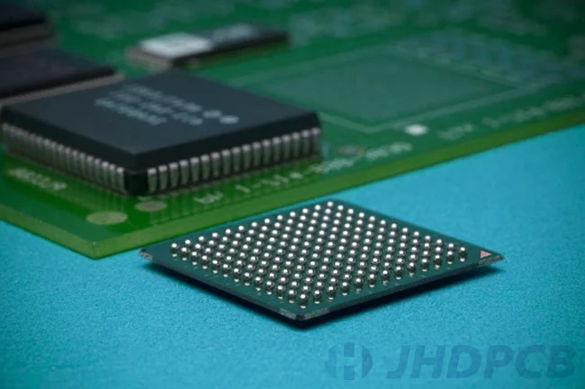
Wire bonding and printed circuit boards (PCBs) are two different processes used in the assembly of semiconductor devices. However, wire bonding is often used to make connections between a semiconductor device and a PCB.
When a semiconductor device is manufactured, it is typically mounted onto a substrate or package using wire bonding. The wire bonds are then connected to the PCB using a variety of methods, including soldering, flip-chip bonding, or conductive adhesive.
In some cases, the PCB itself may be manufactured using wire bonding techniques. For example, some flip-chip packages use wire bonding to connect the semiconductor die to the package substrate. In such scenarios, the wire bonds act as the electrical links connecting the die to the substrate, which is essentially a tiny printed circuit board (PCB).
Overall, wire bonding and PCBs are both important processes in the assembly and manufacturing of semiconductor devices. While they are distinct processes, they often work together to create reliable and high-quality electronic components.

Flip chip vs Wire bond.

Flip chip and wire bonding are two commonly used methods in microelectronics for creating electrical connections between integrated circuits (ICs) or semiconductor devices and their respective packaging or substrates.
Wire bonding is a process that uses thin wires, typically made of gold or aluminum, to create conductive paths between the bonding pad on the IC and the package or substrate. The wire is bonded to the pad using heat and pressure, creating a permanent connection.

flip chip vs wire bond

Flip chip, on the other hand, involves flipping the IC and placing its contacts directly onto the substrate or package. The contacts are typically made of solder bumps or copper pillars, which form the electrical connection when they melt and bond during reflow.
In comparison, flip chip typically offers better electrical performance due to shorter interconnect lengths and higher input/output density. It also allows for higher integration levels, enabling more components to be packed into a smaller area. Wire bonding, on the other hand, is generally less expensive, easier to implement, and more flexible in terms of design and customization.
Both flip chip and wire bonding have their respective advantages and disadvantages, and the choice of which one to use depends on factors such as cost, performance requirements, design complexity, and production volume.
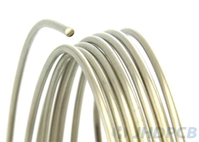
What are the materials used in wire bonding?

Good conductivity, weldability, hardness, and corrosion resistance are necessary for wire bonding materials.Following are the materials and their combinations:

MaterialPropertiesAlloy CombinationsBonding Techniques
Aluminum (Al)Thermal and electrical conductivity, low cost, good workabilityAl-Au, Al-Ni, Al-Si, Al-MgThermosonic bonding
Copper (Cu)Excellent electrical and thermal conductivity, higher strength than AlBall bonding with ultrasonic energy
Silver (Ag)Good thermal and electrical conductivity, low resistivity, high ductilityAg-Au, Ag-Al, Ag-SiCBonding with ultrasonic energy
Gold (Au)Excellent electrical conductivity, ductility, compatibility with silicon chipAu-Al, Au-Cu, Au-PdThermocompression bonding, thermosonic bonding

Aluminum

Aluminum wire is a common choice for thermosonic bonding in semiconductor packaging due to its thermal and electrical conductivity, low cost, and good workability. However, pure aluminum is relatively soft and difficult to draw into fine wires. Therefore, small-diameter aluminum wires are usually alloyed with other metals, such as nickel or gold, to provide higher strength and better adhesion.
Some commonly used wire-pad material combinations in aluminum wire bonding include Al-Au (Aluminum-Gold) and Al-Ni (Aluminum-Nickel). During the bonding process, heat and pressure are applied to the wire to create a metallurgical bond between the wire and the bonding pad on the chip. The bonding parameters, such as temperature, time, and force, need to be carefully controlled to ensure consistent and reliable bonding.
To improve the mechanical properties of aluminum bonding wire, small amounts of silicon or magnesium are often added as strengthening agents. Aluminum-silicon (Al-Si) and aluminum-magnesium (Al-Mg) alloys are commonly used in semiconductor packaging due to their high strength, good ductility, and low coefficient of thermal expansion (CTE), which is important for ensuring reliability under thermal cycling conditions.

Copper

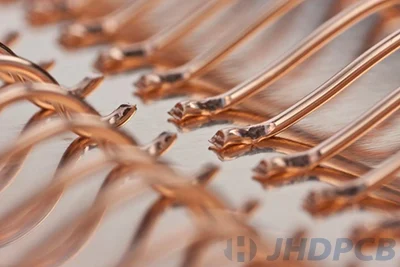
Copper is one of the most commonly used materials for semiconductor wire bonding due to its excellent electrical and thermal conductivity, higher strength compared to aluminum, and lower resistivity. Copper wire has a larger diameter than aluminum wire, making it suitable for high-current applications where large amounts of current need to be passed through the wires.
Ball bonding using copper wire is a widespread approach for fine wire bonding, typically used for wires ranging in size from 10 to 100 micrometers. The process involves creating a small ball at the end of the wire by applying heat and pressure, and then using ultrasonic energy to bond the ball to a metal pad on the semiconductor chip. The small size of the copper wire can help to reduce the footprint of the final device, increasing its density and functionality.
However, copper wire is prone to oxidation when exposed to air, which can lead to poor wire bonding quality and reliability issues. Therefore, ball bonding with copper wire must be done in an inert atmosphere, such as nitrogen or argon, to prevent oxidation and ensure consistent bonding results.
Thus, copper wire is a highly desirable material for semiconductor wire bonding due to its excellent electrical and thermal properties and larger diameter for high-current applications. However, careful handling and processing are required to prevent oxidation and maintain high-quality wire bonding results.

Silver

Silver (Ag) wire is another commonly used material for semiconductor wire bonding due to its good thermal and electrical conductivity, low resistivity, and high ductility. Silver wire bonding can provide a robust and reliable electrical connection in various device applications.
Some suitable wire-pad material combinations for silver wire bonding include Ag-Au (silver-gold), Ag-Al (silver-aluminum), and Ag-SiC (silver-silicon carbide). These combinations can provide good intermetallic bonding and reduce the risk of corrosion or oxidation.
During the wire bonding process, a small ball is formed at the end of the wire using heat and pressure, and then ultrasonic energy is applied to bond the ball to the metal pad on the semiconductor chip. The bonding parameters for silver wire bonding, such as temperature, time, and force, need to be optimized to ensure consistent and reliable bonding results.
One of the advantages of silver wire bonding over copper wire bonding is the absence of oxidation issues, which makes silver wire bonding less sensitive to processing conditions and more forgiving in terms of handling and storage.
To conclude, silver wire is a popular material for semiconductor wire bonding due to its good thermal and electrical conductivity, high ductility, and compatibility with various wire-pad material combinations. Ag-Au, Ag-Al, and Ag-SiC combinations are commonly used in silver wire bonding processes and provide good bonding quality and reliability.

Gold

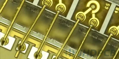
Wire bonding is a crucial step in semiconductor device fabrication, which involves creating electrical connections between the chip and its external leads. Gold wire is one of the most popular materials used for wire bonding due to its excellent electrical conductivity, ductility, and compatibility with the silicon chip.
Pure gold wire can be too soft for some applications, so it is often alloyed with other elements to enhance its mechanical properties. The most widely used combinations are Au-Al (gold-aluminum), Au-Cu (gold-copper), and Au-Pd (gold-palladium). These alloys offer improved tensile strength, thermal stability, and adhesion to the metal pads on the semiconductor chip. Gold plating thickness is crucial in wire bonding, as it determines the quality and reliability of the bond. It affects adhesion, conductivity, and corrosion resistance, and a recommended range of 1-3 microns is typical. Gold plating thickness is critical for a strong and dependable bond, making it a vital aspect of wire bonding.

Thermocompression bonding and thermosonic bonding are two common techniques used for gold wire bonding. Thermocompression bonding involves applying heat and pressure to the bonding wire to form a metallurgical bond with the metal pad on the chip. In contrast, thermosonic bonding uses ultrasonic energy and heat to create a strong bond between the wire and the pad. The quality of the surface finish and cleanliness of the bonding wire and the metal pad is crucial for achieving strong bond formation and preventing capillary clogging during the wire bonding process. Contaminants such as oxides, fingerprints, or grease on the surface can adversely affect bond formation, reduce adhesion strength, and cause capillary clogging. Therefore, proper cleaning and handling procedures must be followed to ensure a clean, well-prepared bonding surface.

In summary, gold bonding wire is an essential material for wire bonding in semiconductor device fabrication due to its excellent electrical properties and ductility. Other elements are often added to gold wire to improve its mechanical properties. Surface finish and cleanliness are critical factors that can affect bond formation and prevent capillary clogging, and proper cleaning and handling procedures must be followed.

What are the types of wire bonding processes?

Wire bonding is a vital step in the manufacture of semiconductor devices. There are two main categories of wire bonding processes: process methods and bonding shapes. Process methods refer to the techniques used to bond the wire to the semiconductor chip. The three primary types of process methods for wire bonding are:
Wire Bonding Process Type
Wire bonding Temperature (oC) Pressure Wire Ultrasonic energy Applications
Thermocompression 300 – 500 High Au No Fine wire to small metal pads, multimetal connections
Ultrasonic 25 Low Au, Al Yes Fine wire to small metal pads, multimetal connections
Thermosonic 100 – 150 Low Au Yes Heavy wires to large metal pads, multimetal connections

Thermocompression bonding

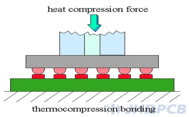
Thermocompression bonding is a process used in semiconductor manufacturing to create a bond between a metal wire and a metal pad on a semiconductor chip. During this process, localized heat is generated by applying high temperature and pressure to the bonding wire and metal pad. The heat softens the materials, allowing them to deform and diffuse into each other. Under high pressure, the softened wire is bonded to the metal pad, creating a metallurgical bond.
Thermocompression bonding is widely used because it provides a reliable, high-strength bond with excellent electrical conductivity. It is particularly useful for bonding fine wires to small metal pads and for creating multimetal connections.
To ensure a successful bond, several factors such as the surface finish, cleanliness, and oxide layer on the metals being bonded must be carefully controlled. The temperature, pressure, and time duration play critical roles in determining the quality and reliability of the bond. The process requires precise control of the bonding tool, temperature, and pressure, which must be optimized for each application.
The thermocompression bonding process has been employed in the semiconductor industry for numerous years and is a crucial method for producing durable electrical connections in various electronic devices.

Ultrasonic bonding

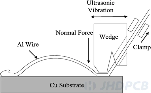
Ultrasonic bonding is a process used in semiconductor manufacturing to create a bond between a metal wire and a metal pad on a semiconductor chip. In this process, the wire is held in place over the pad, and ultrasonic energy is focused on the wire using a transducer. The ultrasonic vibration creates friction and generates heat, softening the materials and causing them to bond together.
ultrasonic wire bonding is widely used because it provides a non-destructive, high-strength bond with excellent electrical conductivity. It is particularly useful for bonding fine wires to small metal pads and for creating multimetal connections.
To ensure a successful bond, several factors such as the surface finish, cleanliness, and oxide layer on the metals being bonded must be carefully controlled. The ultrasonic frequency, amplitude, and duration must be optimized for each application, along with other parameters like force and wire bond deformation.
Ultrasonic bonding is a flexible and versatile process that can create strong bonds between a variety of different metals. It is commonly used in the production of many types of electronic devices, including integrated circuits, sensors, and memory chips.
Overall, ultrasonic bonding is an important technique for creating robust electrical connections in a wide range of electronic devices, and continues to play a significant role in the semiconductor industry.

Thermosonic bonding

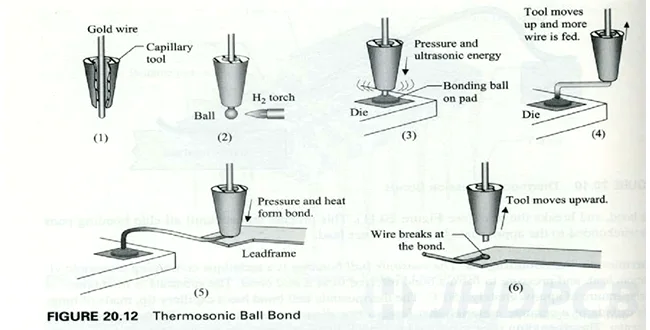
Thermosonic bonding is a process used in semiconductor manufacturing to create a bond between a metal wire and a metal pad on a semiconductor chip. This process is a combination of two other bonding methods, thermocompression bonding and ultrasonic bonding. In thermosonic bonding, both heat and ultrasonic energy are applied to the metal wire and metal pad to create a bond.
During thermosonic bonding, the wire is first heated to soften it, and then ultrasonic energy is applied to the wire while it is pressed against the metal pad. The ultrasonic vibrations create friction between the wire and the pad, producing heat that helps to further soften and activate the materials. Under pressure, the softened materials bond together, creating a strong metallurgical bond.
Thermosonic bonding is a highly effective process because it combines the advantages of both thermocompression and ultrasonic bonding. It is particularly useful for bonding heavy wires to large metal pads or for creating multimetal connections. The process requires less pressure and thermal energy than pure thermocompression bonding, and the ultrasonic energy helps to create a strong and consistent bond.
To ensure a successful bond, several factors such as surface finish, cleanliness, and oxide layer on the metals being bonded must be carefully controlled. The temperature, pressure, and duration of both the heat and ultrasonic energy must be optimized for each application.
Wire bonding in microelectronics is an essential process that enables the creation of reliable and efficient electrical connections. Thermosonic bonding is widely used in the semiconductor industry to produce reliable and robust electrical connections in a variety of electronic devices, including integrated circuits, power devices, MEMS sensors, and other microelectronic components.
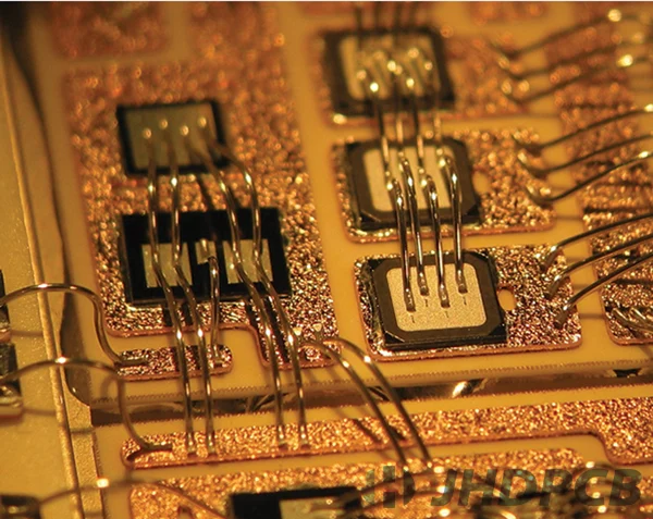
Wire Bond Shape.

Different wire bonding techniques will produce different bond shapes. Bonding shapes refer to the shape of the bonding wire after it has been connected to the chip. There are three main types of bonding shapes in wire bonding:
Wire Bonding Shapes Description Applications
Ball bonding Small metal ball formed at end of wire, applied to metal pad with pressure and heat Integrated circuits, memory chips, microelectronic devices
Wedge bonding Wedge-shaped tool presses wire onto metal pad under pressure Integrated circuits, sensors, memory chips
Stitch bonding Ultrasonic energy and heat create series of loops along bonded wire for added mechanical strength Heavy wire bonding, critical applications requiring reliability

Ball bonding

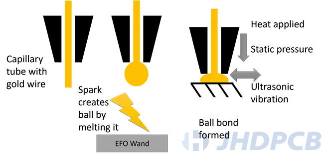
Ball bonding is a process used in semiconductor manufacturing to create a bond between a metal wire and a metal pad on a semiconductor chip. In this process, a small ball of metal is first formed at the end of a thin wire using thermal or electrical energy. The ball is then placed over the metal pad, and pressure and heat are applied to bond the ball to the pad.
During ball bonding, the wire is first threaded through a capillary, which helps to guide it to the correct location on the semiconductor device. Once the ball is formed at the end of the wire, the capillary moves the ball into position over the metal pad. Pressure and heat are then applied to create a bond between the ball and the pad.
Ball bonding is widely used because it can produce a high-strength bond with excellent electrical conductivity. It is particularly useful for bonding fine wires to small metal pads, making it a common technique for producing interconnections in integrated circuits, memory chips, and other microelectronic devices.
To ensure a successful bond, several factors such as the surface finish, cleanliness, and oxide layer on the metals being bonded must be carefully controlled. The temperature, pressure, and duration of the bonding process must be optimized based on the materials being used.
The ball bonding technique has been widely implemented in the semiconductor industry for numerous years. It is an important technique for creating reliable and robust electrical connections in a wide range of electronic devices.

Wedge bonding is a process used in semiconductor manufacturing to create a bond between a metal wire and a metal pad on a semiconductor chip. In this process, a small wedge-shaped tool is used to press the end of a thin wire onto the metal pad, creating a bond under pressure.
During wedge bonding, the wire is first threaded through a capillary that helps to guide it to the correct location on the semiconductor device. Once the wire is positioned over the metal pad, a wedge-shaped tool is used to press the wire down onto the pad with a specific amount of force. This creates a strong metallurgical bond between the wire and the pad.
Wedge bonding is widely used because it can produce a high-strength bond with excellent electrical conductivity. It is particularly useful for bonding fine wires to small metal pads and for creating multimetal connections.
To ensure a successful bond, several factors such as the surface finish, cleanliness, and oxide layer on the metals being bonded must be carefully controlled. The force applied by the wedge tool must also be optimized based on the materials being used.
The wedge bonding method is a widely accepted process that has been utilized in the semiconductor industry for many years. It is an important technique for creating reliable and robust electrical connections in a wide range of electronic devices, including integrated circuits, sensors, and memory chips.
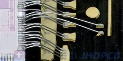
Stitch bonding is a wire bonding technique that creates a series of loops along the wire after it has been bonded to the chip. This method provides improved mechanical strength and is typically used in heavy wire bonding applications or instances where additional support is needed.
Stitch bonding involves using ultrasonic energy and heat to create a series of loops along the bonded wire. These loops provide additional support and flexibility, improving the overall reliability and longevity of the bond. Stitch bonds can be used with various wire materials, including copper, gold, and aluminum.
One notable advantage of stitch bonding is its ability to enhance the mechanical stability of the bond. The loops created by stitch bonding distribute the stress and strain applied to the bond over a larger area, reducing the chance of failure due to mechanical stress. For this reason, stitch bonding is often used in critical applications where the reliability of the bond is of utmost importance.
Moreover, stitch bonding can also improve the electrical performance of the bond by reducing contact resistance and increasing the bond strength between the wire and the pad. Additionally, stitch bonding can be used to create complex shapes and patterns for specific applications, making it a versatile technique in the field of wire bonding.
Overall, stitch bonding is a valuable technique in the wire bonding industry. Its ability to provide added mechanical strength and flexibility makes it a reliable choice in applications where high-performance and dependability are necessary.

How to choose the right wire bonding process?

When selecting wire for bonding, several factors should be considered. These include the maximum current limit, cost, and wire bond pitch.
Gold wire with a 1-mil diameter is commonly used by designers. It has an electrical resistance of approximately 1.17 mΩ per mil and a maximum current limit of around 0.7 A, depending on factors such as heatsinking and wire length.
The inductance value of a gold wire bond with a diameter of 1-mil is usually about 25 picoH per mil, although this can fluctuate based on the height of the bond wire. Wedge bonding typically involves the use of aluminum wire. However, because of its high affinity to oxidize, ball bonding with aluminum wires should be performed in an inert environment.
When choosing wire for bonding, cost is also a crucial factor to take into account. Gold wire is more expensive than aluminum wire, but it provides better performance in terms of reliability and electrical conductivity. Designers must balance these factors to select the best wire for their specific application.
As a result, when selecting wire for bonding, designers should consider factors such as maximum current limit, cost, wire bond pitch, and the specific application requirements to ensure optimal performance and reliability.

ApplicationsWedge BondingBall Bonding
Bonding TechniquesThermosonic, UltrasonicThermocompression, Thermosonic
TemperatureAu wire: T/S 120o – 200oCAl wire : U/S room temperatureT/S : 120o – 200oCT/C : 300o C
Pad sizeSmaller size ofpad than ball bond. High performance in microwave usage. Pad size is around 2 or 3 times wire diamieterAround 3 or 5 times of wire diameter
Wire sizeAny size ribbon or wireSmall or < 75 µm
Wire materialAl, AuAu
Pad materialAl, AuAl, Au
Speed4 wires/secUp to or more than 12 wires/sec

Procedures and precautions for wire bonding.

Wire bonding is a critical process in electronics manufacturing, and it requires precise equipment and skilled technicians to achieve reliable and high-quality results. At JHDPCB, we have a team of experienced professionals and state-of-the-art wire bonding equipment to ensure that we can meet even the most demanding wire bonding requirements.
Our wire bonding capabilities include ball bonding, wedge bonding, and stitch bonding, and we can work with a range of wire materials, including gold, copper, and aluminum. We also take great care to ensure that our wire bonding procedures follow best practices and industry standards to minimize the chances of defects and failures.
At JHDPCB, we understand the importance of wire bonding in electronic products, and we are committed to providing our customers with top-quality wire bonding services. Whether you need wire bonding for a new product prototype or for mass production, we have the expertise and equipment to get the job done right. Choose JHDPCB for your wire bonding needs and experience the high level of precision and quality that we bring to every project.

  • Keep bond pad size and placement consistent: Bond pad size and placement should be consistent across all devices to ensure that the bonding wire can be placed accurately and reliably.
  • Choose the right wire diameter and material: Select a wire diameter and material that is appropriate for the application. Factors to consider include electrical conductivity, hardness, and corrosion resistance.
  • Control wire length and loop height: Wire length and loop height should be consistent across all connections to ensure uniformity and minimize stress on the bonds.
  • Minimize loop count: A lower loop count will reduce the overall length of the bonding wires, which can result in better performance and reliability.
  • Avoid sharp turns: Wire bonding is sensitive to sharp turns, which can cause damage to the wire or substrate. Use gentle curves or loops instead.
  • Provide adequate clearance: Provide enough clearance between the bonding wire and other components to avoid interference.
  • Use appropriate adhesive: Select an adhesive that is suitable for the application and the materials being bonded.
  • Optimize thermal management: Thermal management is important during the bonding process to prevent damage to the substrate or components. Proper heat sinking and thermal control can help to ensure consistent and reliable bonds.

By keeping these design tips in mind, you can optimize the wire bonding process and increase the reliability and performance of your semiconductor devices.

IC placement is a critical step in the wire bonding process. Here are some tips for successful IC placement:

  1. Use precision placement equipment: High-quality placement equipment ensures accurate positioning of the IC on the substrate or package.
  2. Follow the manufacturer’s guidelines: The IC manufacturer may provide guidelines for proper placement and handling of the IC.To prevent harm or incorrect alignment, make sure to adhere to these instructions.
  3. Use appropriate adhesives: Select an adhesive that is suitable for the application and the materials being bonded. Make sure to apply a small amount of adhesive to each bond pad to hold the IC in place during the bonding process.
  4. Verify alignment: Once the IC is placed on the substrate, verify its alignment with the bond pads using a microscope or other imaging system. Verify that the bond pad positions on the IC coincide with those on the substrate.
  5. Consider thermal management: IC placement can affect thermal management in the final device. Consider factors such as heat dissipation and thermal expansion when placing the IC.
  6. Optimize routing: When positioning the IC, consider the routing of the bonding wires. Avoid routing wires over sensitive areas or sharp corners.
  7. Minimize stress: Avoid placing the IC too close to other components or features that could cause stress on the device during operation.

By following these tips, you can ensure proper IC placement and increase the success rate of the wire bonding process.

Wire bonding is a precise procedure that necessitates meticulousness and cautious manipulation. Here are a few measures to bear in mind when carrying out the wire bonding process:

  1. Cleaning: The first step in the wire bonding process is to clean the substrate surface and the bonding pads to remove any contaminants that might interfere with the bonding process.
  2. Alignment: The next step is to align the wire bonding tool with the bonding pad. This ensures that the wire will be bonded to the correct location on the substrate.
  3. Wire bonding: Once the alignment is complete, the wire bonding tool is used to bond the wire to the bonding pad. This is generally accomplished via a blend of heat, force, and ultrasonic waves.
  4. Wire looping: After the wire is bonded to the bonding pad, it is looped around to connect to the next bonding pad. This looping process is repeated until all of the bonding pads are connected.
  5. Wire cutting: Once all of the bonding pads are connected, the excess wire is cut using a wire cutter. This ensures that the wire is the correct length and that there are no loose ends that could cause problems later on.
  6. Inspection: Finally, the completed wire bond is inspected to ensure that it meets the required specifications. This involves inspecting for any flaws or problems that may impact the final product’s functionality.

These steps are repeated for each device being manufactured. The wire bonding process requires precision and attention to detail in order to achieve reliable connections and high-quality semiconductor devices.

Wire bonding is a precise procedure that necessitates meticulousness and cautious manipulation.Here are some precautions to keep in mind during the wire bonding process:

  • Cleanliness: Ensure that all tools, surfaces, and materials are clean and free of contaminants, such as dust, oil, or fingerprints. This minimizes the risk of defects and ensures reliable bonds.
  • ESD protection: Use proper ESD (electrostatic discharge) protection to prevent damage to sensitive components and ensure proper operation of the equipment.
  • Bonding wire handling: Handle bonding wire with care to avoid kinking, torsion, or other damage. Use only the amount of wire needed for each bond to minimize waste and minimize stress on the connection.
  • Capillary handling: Capillaries should be handled carefully to avoid damage or contamination that could affect the bonding process.
  • Temperature control: The wire bonding process can be sensitive to temperature fluctuations. Proper temperature control can help ensure consistent and reliable bonds.
  • Bond pad readiness: Verify that the bond pads are spotless and devoid of any oxides or pollutants that could obstruct the bonding procedure.
  • Conductivity: Check the electrical conductivity of the bond pads to ensure that they meet specifications.
  • lQuality control: Inspect the wire bonds using a microscope or other visualization system to ensure that they have been formed properly and that there are no defects or damage.

By following these precautions, you can minimize the risk of defects and ensure reliable and high-quality wire bonds.

What are the methods for testing wire bonds?

The acceptability of wire-bonded components and the strength of wire bonds can be evaluated using either a DPT/Destructive Pull Test or an NDPT/Non-Destructive Pull Test. The most commonly used standard is MIL-STD-883, which includes Method 2011.7 for Bond Strength Method 2023.5. These standards specify sample sizes for each test type and acceptance criteria for different bonding and wire types. A few assessment test that is recorded in this standard such as:

  • Internal visual: This test involves inspecting the wire bonds using a microscope or other visualization system to detect any visible defects, such as incomplete bonds or cracks.
  • Nondestructive bond pull test: This test measures the strength of the wire bond by applying tension to the wire without breaking it. The bond must withstand a specified force to pass this test.
  • Destructive bond pull test: Similar to the nondestructive bond pull test, this test measures the strength of the wire bond but involves breaking the bond to determine its maximum strength.
  • Mechanical shock: This test simulates the effects of mechanical shock on the device and checks for any damage to the wire bonds.
  • Ball bonding shear test: This test measures the strength of ball bonds, which are used in certain types of wire bonding, by applying a shear force to the bonded ball.
  • Stabilization bake: This test involves exposing the device to high temperatures to simulate the effects of aging and check for any changes in wire bond strength or reliability.
  • Constant acceleration: This test simulates the effects of constant acceleration on the device and checks for any changes in wire bond strength or reliability.
  • Moisture resistance: This test simulates exposure to moisture and checks for any changes in wire bond strength or reliability.
  • Random vibration: This test simulates random vibration and checks for any changes in wire bond strength or reliability.

In electronics manufacturing, testing wire bonds is an essential step to ensure the reliability and quality of the final product. At JHDPCB, we have a range of testing methods available to us to verify the integrity of wire bonds and ensure that they meet the required specifications.

As a leading provider of PCB manufacturing services, JHDPCB is committed to delivering high-quality products and services to our customers.With our advanced manufacturing facilities and skilled team, we are capable of delivering dependable and effective wire bonding solutions for a diverse array of semiconductors. Join us on an enlightening journey through the intricacies of wire bonding, as we uncover the immense value it brings to the world of PCB manufacturing and how JHDPCB’s capabilities ensure unparalleled quality and performance.
Whether you need wire bonding for flip-chip packages, wire bonding for die attachment, or other applications, we have the expertise and capabilities to deliver results that meet your exact specifications. Our commitment to quality and customer satisfaction is evident in everything we do, from our rigorous testing processes to our use of advanced materials and technologies.
At JHDPCB, we take pride in our ability to manufacture innovative and reliable products that meet the needs of our customers. If you require a reliable collaborator for your wire bonding requirements, JHDPCB is the perfect choice. Reach out to us today to acquire more information regarding our wire bonding expertise and how we can support you in accomplishing your objectives.

Get a PCB Quote Now

Open high-quality PCB manufacturing services in JHDPCB

Leave a Comment