HDI-PCB-blog

Fully understand HDIPCB

directory

Definition of HDI PCB.

In order to comply with the development of the technological world, PCBs need to pack more functions into smaller packages. HDI PCB is a printed circuit board with a higher wiring density per unit area than traditional printed circuit boards, which means that the same HDI PCB tends to have smaller products and faster speeds. HDI PCB uses blind vias, buried vias and microvias, vias in pads, and very fine traces to encapsulate more components into a smaller area. Therefore, HDI PCB is defined as a PCB with one or all of the following functions. One HDI board can accommodate the functions of the previously used PCB instead of using several PCBs in the device.

The benefits of HDI printed circuit boards.

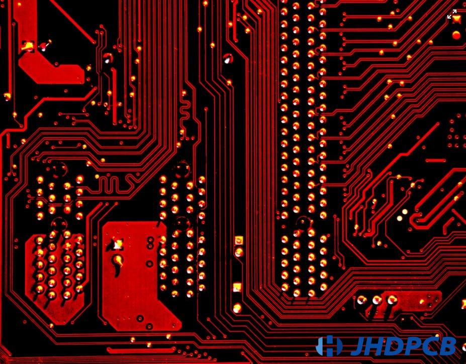
The main advantage of HDI printed circuit boards is that they can “do more with less”; HDI PCBs shorten the distance between the equipment and the wiring space, allowing the deployment of a large number of circuits to improve the performance of electronic products while reducing power consumption. Due to shorter connection distances and lower power requirements, signal integrity has also been improved. Other performance improvements compared to traditional PCBs include stable voltage rails, smallest stubs, lower RFI/EMI, tighter ground planes, and distributed capacitance.

The following benefits can also be obtained by using HDI printed circuit boards:

  • Cost-effectiveness: Proper design in the early stage. Compared with standard PCBs, the overall cost will be reduced due to the smaller number of layers and the smaller size/the number of circuit boards required under the same implementation effect.
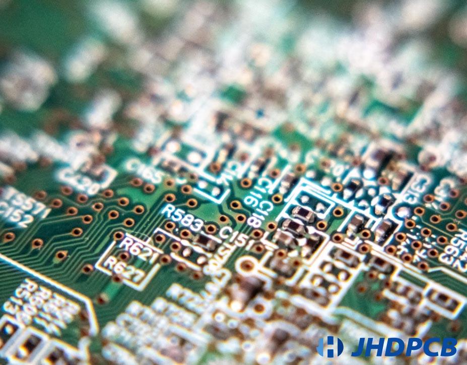
  • Better reliability: Due to the use of a smaller aspect ratio, micro-vias have better reliability than typical vias; they are more reliable than vias, and better materials and parts are used to give HDI excellent performance.
  • Faster time to market: Design efficiency in HDI PCB production means faster time to market. Due to the easy placement of components and vias and electrical performance, the design and testing process of HDI PCB requires a shorter time.

HDI-PCB

Common uses of high-density interconnect printed circuit boards.

Due to the excellent performance of HDI PCB, it is usually used in more complex electronic devices, which require excellent performance while saving space. Applications include mobile/cellular phones, touch screen devices, notebook computers, digital cameras, 4/5G network communications, and military applications such as avionics and smart ammunition.

Automotive and aerospace industries: Lighter weight means higher operating efficiency, so HDI PCBs are increasingly used. Like almost everything else, cars are becoming more and more interconnected and computerized. Many advanced features, such as in-vehicle WiFi and GPS, rear-view cameras and backup sensors, rely on HDI PCB. Today’s cars have about 50 microprocessors, which play a role in engine control, diagnostics, safety functions, and other conveniences. With the continuous advancement of automotive technology, HDI​​ technology may play an increasingly important role.

Industrial manufacturing: Industrial automation requires a lot of computerization, and IoT devices are becoming more and more common in manufacturing, warehousing and other industrial environments. Many of these advanced devices use HDI technology. Today, companies use electronic tools to track inventory and monitor equipment performance. More and more machines include smart sensors that collect usage data and connect to the Internet to communicate with other smart devices, as well as pass information to management and help optimize operations.

Medical equipment: HDI PCB also occupies a prominent position in medical equipment; advanced electronic medical equipment, such as monitoring, imaging, surgery, laboratory analysis and other equipment, all include HDI boards. High-density technology promotes improved performance and smaller, more cost-effective devices, potentially improving the accuracy of monitoring and medical testing.

At JHDPCB, we continue to introduce the latest equipment and technology to manufacture high-quality HDIPCB at the forefront of the industry. To meet any of your PCB project needs; we can provide up to 20 layers of printed circuit boards, and up to 20 ounces of copper weight. Whether it is HDI PCB with blind vias, buried vias or special plating processes, the quick quotation function and online customer service of JHDPCB can provide fast quotations for your PCB customization projects. Or you can do it by emailing your requirements or Gerber files to sales@jhdpcb.com.
Learn more about JHD’s HDI PCB manufacturing capabilities.

Explore more JHDPCB blogs

Leave a Comment