PCB Package
directory
What is PCB Package Technology?
PCB electronic kit assembly is the most important factor for the rapid growth of the electronic systems industry. The electronics industry has grown at a very high rate since the introduction of integrated circuits in the late 1950s. So today, we can have a simple electronic board that runs faster than the computers that took up entire rooms in the 1940s.
The size reduction and high performance of electronic systems is due to the integration and packaging of electronic circuits and device assemblies. IC package can have millions of transistors that can perform a large number of functions in a small area. The package substrate PCB can realize the interconnection between different ICs on the same substrate. PCB packaging provides mechanical, thermal support, and electrical interconnection between the bare pcb packaging board and various ICs and discrete components, enabling them to operate as a single system unit. Today, PCBs can be found in almost all electronic systems and devices, such as computers, cell phones, watches, and more.
PCB package function: Due to the consistency of similar printing boards, manual wiring errors can be avoided, and it can be automatically inserted or installed. Therefore, after the electronic device is printed, automatic welding and automatic detection of electronic components can be achieved. So as to ensure electronic quality equipment, improve labor productivity, reduce costs and promote maintenance.
What types of PCB packages are there?
According to application requirements, pcb package are classified into various types. Before choosing a PCB, you must consider considerations including required space, stress handling, mechanical, electrical stability and so on.
Common PCB package types are divided into the following: SMT, PGA, DIP, LCC, BGA, QFN package, QFP package, TSOP, CSP package.
SMT Package
One method of mounting electronic components directly to the surface of a printed circuit board is surface mount technology(SMT). This method has largely replaced the through-hole technology construction of assembled components in the industry. SMT can improve manufacturing automation, thereby reducing costs, and improving quality is the main reason.It also allows more components to be mounted on a given substrate area, allowing both technologies to be used on the same board. However, in large transformers and thermal power semiconductors that are not suitable for surface mount components, we usually use through-hole technology.
SMD components are generally smaller than through-hole components because they have smaller leads or none. It may have various styles of short pins or leads, flat electrical contacts, solder ball (BGA) matrix, or termination on the component body.
Compared with the older through-hole technology, the main advantages of SMT are as follows:
- Have smaller components;
- Have element density (number of elements per unit area) and more connections per element;
- We can place components on both sides of the circuit board;
- Higher connection density, because the holes will not block the wiring space of the inner layer. If the components are only installed on one side of the PCB, they will not block the back layer;
- Small errors in component installation will be automatically corrected because the surface tension of molten solder will pull the component to the position aligned with the pad. (on the other hand, the through-hole element cannot be slightly misaligned, because once the lead passes through the hole, the element is fully aligned and cannot be displaced laterally.)
- Better mechanical performance under impact and vibration conditions (partly due to smaller mass and partly due to fewer cantilever beams)
- Lower resistance and inductance at the connection; Therefore, the unwanted RF signal has less influence, and the high-frequency performance is better and more predictable.
- Better EMC performance (lower radiation emission) due to smaller radiation loop area (due to smaller package) and smaller lead inductance;
- It needs to drill fewer holes. (drilling PCB is time-consuming and expensive, Click to view detailed PCB via types.)
- Use automated equipment to reduce the initial cost and setup time of mass production;
- Simpler and faster automated assembly. Some mounters can mount more than 136000 components per hour;
- Many SMD parts cost less than equivalent through-hole parts.
PGA Package
A pin grid array (PGA) is one of many integrated circuit packages. In a PGA package, the pins are usually arranged in a square or rectangular pattern on the bottom of the package in a regular array. These pins are typically 2.54 mm (0.1 in) pitch, and the entire bottom surface of the package can be optionally covered or uncovered.
On a printed circuit board or plugged into a socket, PGAs are typically mounted using the through-hole method. Compared with the old package, PGA allows more pins per integrated circuit.
The advantages of PGA package are:
- Small footprint;
- Good heat dissipation;
- Impedance due to the short connection path to the circuit board;
- It can be easily removed from the circuit board without damaging the chip;
- The chip can be soldered to a new circuit board for recycling.
BGA Package
A type of surface mount device (SMD) component without leads is called a ball grid array integrated circuit. This SMD package uses a set of metal balls made of solder, called solder balls, for connection to a PCB (printed circuit board). These solder balls are attached to the laminate substrate on the bottom of the package.(For more substrate types, please click here.)
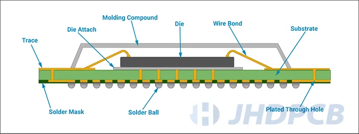
Figure 1: Chips connected toBGA by wire bonding;
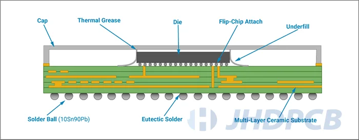
Figure 2: Die connected to the BGA using Flip-chip technology.
Figures (1) and (2) show two examples of how to build a BGA device. Figure (1) shows how mounts the BGA die/chip on the substrate and connects to the substrate using wire bonding technology. Figure (2) shows how to connect the BGA die to the substrate using flip-chip technology.
BGA chip connections are connected to solder balls using metal traces on the substrate. BGA packages can provide more Inconnections than dual in-line or flatpack.
The connection from the die to the ball in the BGA IC is on average shorter than the peripheral type connection such as the dip IC. Therefore, better performance can be obtained at high speed.
Features of BGA:
- High lead count;
- No leads to bend;
- High interconnection density;
- Occupies lesser space on the board;
- Low inductance;
- Self centering during reflow to reduce placement problems during surface mount welding;
- The thermal resistance is lower between the package and the PCB. This makes it easier for the heat generated by the integrated circuit in the package to flow to the PCB and prevent the chip from overheating.
DIP Package
In microelectronics, DIP or DIL is an electronic component package, which has a rectangular shell and two rows of parallel electrical connection pins. Packages can be hole mounted on a printed circuit board (PCB) or plugged into a socket. The DIP format was invented in 1964 by Don Forbes, Rex Rice and Bryant Rogers of Fairchild Research and Development. At the time, the use of integrated circuits was limited due to the limited number of leads available on circular transistor packages. More and more complex circuits require more signal and power lines (as indicated by the rental rule); eventually, microprocessors and similar complex devices require more leads than immersion packages, enabling the development of higher density chip carrier.
Dip is usually referred to as dip n, where n represents the total number of pins. Let me give you an example, a microcircuit package with two rows of four vertical leads would be DIP 8. The image below shows a DIP8 IC. Ordinary packages need at least three and at most 64. Many analog and digital integrated circuit types use DIP packages, as well as transistors, switches, light emitting diodes and resistor arrays. The immersion plug of the ribbon cable can be used with the standard IC socket.
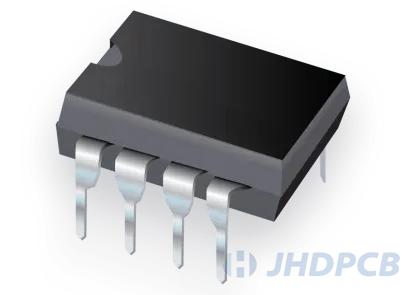
Dip packages are usually made of opaque molded epoxy plastic and pressed around tin, silver or gold-plated lead frames that support the device chip and provide connection pins. Some types of ICs are manufactured using ceramic dip packages, which require high temperature or high reliability, or devices have an optical window inside the package. Most dip packages are fixed to the PCB by inserting pins into holes on the board and welding them in place. Use dip sockets where parts need to be replaced, such as in test fixtures or where programmable devices must be removed for change. The zero insertion force (ZIF) mechanism is included in some sockets.
Variants of dip packages include those with only a single row of pins, such as a resistor array, which may include a heat sink instead of the second row of pins, and four rows of pins, staggered on each side of the package. Dip packages have been largely replaced by surface mount package types, which avoids the cost of drilling holes on the PCB and allows higher density interconnection.
Its characteristics are:
- Electrical life: test each switch under 24VDC voltage and 25mA current, it is proved that it can be tossed back and forth 2000 times;
- Infrequent switching rated current: 100mA, withstand voltage 50VDC;
- The rated voltage and current of the constant switch switch: 25mA, resistant to 24VDC;
- Contact Impedance: 50mΩ maximum is (a) Initial value;(b) After testing, we found a maximum value of 100mΩ;
- Insulation resistance: the minimum insulation resistance is 100mΩ, 500VDC;
- Compressive strength: 500VAC/1 minute;
- Polar capacitance: maximum 5pF;
- Circuit: Single-contact radio: DS(S), DP(L).
LCC Package
An integrated circuit package without pins / leads for contact is called leadless chip carrier. This surface mount device uses metal pads on the outer edge to establish connection with the circuit board.Lead-free chip carriers are popular mainly because they are lightweight and suitable for a wide range of applications, making them ideal for surface mount applications.
Advantages of LCC:
- Thin, multi-layer ceramic packaging;
- Footprint compatible with CQJB and PLCC;
- Solder, Glass or Epoxy Seal;
- Castellations instead of external leads;
- Low cost solution for surface mount leadless packages;
- Strong sealing;
- Non-magnetic option available (but does not mean zero tesla)
QFN Package
A QFN is a semiconductor package that connects an ASICC to a PCB by using surface mount technology. Also, a leadframe-based package is a QFN, known as a chip scale package (CSP). This is because after board assembly, it allows you to view and contact potential customers. Typically, copper leadframes make up the QFN package PCB interconnect and die assembly. Additionally, the package can have a single row or multiple rows of pins. In other words, the single-row structure of the package is formed by a sawing or die-cutting process. And both programs split a lot of packages into separate packages. Forthmore, multiple rows of QFNs are copper etched to achieve the preferred pin count and row count. The saw will then destroy the row and pin. what’s more, QFNs typically have an open thermal pad under the package. So if you want the best heat transfer from the chip you can solder the packet directly to the PCB.
Advantages of QFN Packages:
- There is no lead coplanarity problem in the package;
- Small footprint, which helps to save PCB space;
- QFN uses conventional surface mount equipment and processes for PCB assembly;
- The package is relatively thin, that is, the package height of QFN is less than 1mm;
- Excellent thermal performance (considering that it provides an excellent way for heat transfer from the die to the circuit board during soldering);
- The components on the board can be close to the components of QFN because its size, position and shape factor of the contact pad are small;
- QFN has a slight package lead inductance;
- Excellent electrical performance;
- The semiconductor package is affordable.
QFP Package
Quad Flat Package is a package for surface mount, SMD integrated circuits.
QFP is widely used because it enables SMD ICs with a large number of interconnects to be used in electronic circuits.
Quad Flat Package is an industry standard package format, but there are several formats to choose from. These include changes in pin count, as well as changes in other aspects of packaging.
Advantages:
- Utilizes mature technology;
- Can utilize sockets;
- Square QFP packages can accommodate a higher pin density than the rectangular type.
TSOP
A thin small outline package (TSOP) is one of many surface mount IC packages. They are very low profile (about 1 mm) and the lead spacing is very small (as low as 0.5 mm).
Because of the large number of pins and small size, they are often used for ram or flash memory IC. In some applications, they are replaced by ball grid array packages to achieve higher density. The main application of this technology is memory. Manufacturers of SRAM, Flash, FSRAM and E2PROM find this package ideal for their end-use products. It meets the needs of Telecom, cellular, memory module, PC card (PCMCIA card), wireless, netbook and numerous other product applications.
TSOP is the smallest lead dimension in flash memory.
Advantage:
- Small-sized, slim type and light;
- Steady yield performance;
- Lower cost;
- Lead-free.
CSP Package
This is the latest generation of memory chip packaging technology, which can improve its technical performance. CSP packaging can make the ratio of chip area to package area more than 1:1.14, which is quite close to the ideal situation of 1:1. The absolute size is only 32 square mm, about 1 / 3 of ordinary BGA, and only 1 / 6 of the area of TSOP memory chip.
In the same space, the memory capacity of the CSP package is three times that of the BGA package.
CSPs offer advantages like:
- Smaller size (reduced footprint and thickness)
- Lesser weight;
- Relatively easier board assembly process;
- Lower overall production costs;
- Improvement in electrical performance.
| PCB Integrated Circuit Package Type Table | |||||
|---|---|---|---|---|---|
| Terminal Orientation | Package method | Terminal shape | Abbreviation | Full name | Information |
| Single direction | Plug in | linear | SIP | Single In-line Package | The pins are arranged vertically on one side of the component. The number of pins is limited. |
| SSIP | Shrink Single In-line Package | ||||
| HSIP | Thermal single in-line package | ||||
| Fold | ZIP | Zigzag In-line Package | Pins on the same side are arranged vertically and folded over each other in a zigzag shape. It is also possible to directly process the pins into a serrated shape to reduce the pin spacing. Often used as a replacement for DIP and TSOP. | ||
| SZIP | Shrink Zigzag In-line Package | ||||
| 2 directions | Plug in | linear | DIP | Dual In-line Package | An early type of dual inline plug-in IC package. Later it was gradually replaced by SOP. |
| SDIP | Shrink Dual In-line Package | ||||
| CDIP | Ceramic Dual In-line Package | ||||
| WDIP | DIP with Window Package | ||||
| Surface Mount Technology | L shape | SOP | Small Outline Package | The pin spacing of SOP is shorter than that of DIP. It is the most common package type in surface mount technology. If the pins extend from four directions, it is called QFP. | |
| SSOP | Shrink Small Outline Package | ||||
| TSOP | Thin-Small Outline Package | ||||
| TSSOP | Thin-Shrink Small Outline Package | ||||
| MSOP | Mini Small Outline Package | ||||
| QSOP | Quarter Small Outline Package | ||||
| SOIC | Small Outline Integrated Circuit | ||||
| SOICW | Small Outline Integrated Circuit Wide | ||||
| J shape | SOJ | Small Outline J-leaded package | The pins stick out from the sides and then bend inside the box. This reduces the size of the PCB circuit board. | ||
| Electrode Buds | SON | Small Outline Non-leaded package | There are electrode pads on both sides for connection terminals, no pins. If there are pad terminals in all four directions, it is called QFN. | ||
| VSON | Very-thin Small Outline Non-leaded package | ||||
| 4 directions | Surface Mount Technology | L shape | QFP | Quad Flat Package | The pins are gull-winged and protrude from the four sides of the square housing. |
| TQFP | Thin Quad Flat Package | ||||
| STQFP | Small Thin Quad Plastic Flat Package | ||||
| FQFP | Fine-pich Quad Flat Package | ||||
| HQFP | Quad Flat Package with Heat sink | ||||
| LQFP | Low profi le Quad Flat Package | ||||
| VQFP | Very-small Quad Flat Package | ||||
| MQFP | Metric Quad Flat Package | ||||
| J shape | QFJ | Quad Flat J-leaded package | Similar to QFP. It’s just that the tips of the pins are bent inwards to form a J shape. | ||
| Electrode Buds | QFN | Quad Flat Non-leaded | It is an upgraded version of SON. Electrode pads are located in four directions on the bottom. The required area of the package is smaller than that of QFP, which is conducive to the realization of small and high-density connections. | ||
| TQFN | Thin-Quad Flat No-Lead Plastic package | ||||
| LCC | Leaded Chip Carrier | ||||
| CLCC | ceramic leaded chip carrier | ||||
| DFN | Dual Flat package | ||||
| QFI | Quad Flat I-leaded package | ||||
| Contact Mount | Tape and film | QTP | Quad Tape-carrier Package | It belongs to the upgraded version of DTP. Suitable for high-density multi-pin packaging process. | |
| / | Contact Mount | Tape and film | DTP | Dual Tape carrier Package | A resin coating encapsulation process. Tape to connect integrated circuits to circuit wiring using Tape Automated Bonding. |
| Matrix Arrangement | Insert mounting | Needle | PGA | Pin Grid Array | The pins are arranged in a rectangular array. Leading position in the field of multi-pin packaging. |
| CPGA | Ceramic PGA | ||||
| PPGA | Plastic PGA | ||||
| SPGA | Staggered PGA | ||||
| Surface Mount Technology | Solder ball | BGA | Ball Grid Array | Arrange ball solder balls on the bottom of the IC as connecting terminals. BGA can provide more high-density interconnect pins. It has the technical advantages of high welding quality and high efficiency. | |
| EBGA | Enhanced BGA | ||||
| FTBGA | Flex Tape BGA | ||||
| TFBGA | Thin & Fine-Pitch BGA | ||||
| Electrode Buds | LGA | Land Grid Array | Copper electrode pads are arranged in an array on the bottom of the IC as connection terminals. The overall package height is less due to the LGA minus the solder balls. It is an ideal process type for high frequency circuits. | ||
The importance of PCB package.
Nowadays, technology has been integrated into people’s daily life to a large extent. Televisions, computers and cell phones provide people with easy access to information and entertainment. Most devices have a printed circuit board (PCB) in their internal design to keep the device functioning properly, and good packaging technology improves the stability of the PCB function. PCB packaging serves as the final stage of a printed circuit board (PCB). In this process, semiconductor electronic components such as various capacitors, resistors, and various functional chips are packaged in the PCB board to protect the IC from potential external irresistible elements and the corrosive effects of aging. To put it simply, the package is a protective shell. Its main function is to transmit the signal to the electric melting point of the circuit board of the electronic device while protecting the module, so as to realize the stable operation of the function of the PCB board.
Its main functions are as follows:
- The size of the board can be reduced;
- Optimize the stability of the PCB circuit;
- It is beneficial to control the impedance of the circuit; (For detailed impedance control methods, please refer to our other blog.)
- Provide high-density interconnection;
- Multifunctional design can be realized.
Package process considerations.
People rely on technology, but pay little attention to what it is made of, such as circuits, low-loss materials and many other components that enable devices to run smoothly. Just as people depend on devices, devices depend to a large extent on their components. Therefore, in order to choose the right PCB for your PCB project, IC packaging must first understand the technical information of various design considerations in the PCB packaging production process, such as: material composition, substrate and reasonable design. Thus, a more stable product is produced for you.
Traceroute Requirements–
Pin size, spacing, and package pads vary depending on the type of surface mount package. However, all of these and current carrying requirements affect the size and weight of the wiring.
Clearance and Spacing Requirements–
For PCB assembly, adequate clearance and spacing between circuit board components and to the edges of the board is critical to achieve high-quality solder connections.
Welding resistance problem–
Conduct resistance welding in the manufacturing process of circuit board; However, in addition to protecting the surface of the circuit board from oxidation, the solder resist also supports assembly by providing a barrier against solder bridging and other unwanted connections.
By selecting–
PCB drilling is also a manufacturing process. However, the number, type, and location of holes drilled are important for assembly because the components must be accurately aligned with the through holes of the circuit board.
Test accessibility–
Another important issue when using PCB packages is Design for Test (DFT) requirements. Functional tests that may be performed during PCBA require pin access, which is not available for flat packs without leads and gate array PCB packages.
Fine-Tuning Your Component Placement–
In addition to the general guidelines for placing components in basic order, there are other design considerations to note:
1,Direction: it is recommended to set the direction of similar components as one direction to help achieve an efficient and error free welding process.
2,Placement: Stay clear of placing components on the solder side of a board that would rest behind plated through hole components
3,Organization: To limit the number of board assembly steps, ensure that all through-hole components are placed on top of the PCB and surface mount (SMT) components are placed on the same side of the PCB.
Place power, grounding and signal wiring–
After the components are placed, it is time to handle the power, grounding and residual signal routing according to the following guidelines:
1. Position the power supply and ground plane: ensure that the power supply and ground plane are symmetrical, centered and located inside the PCB. In addition, it is recommended to keep the power and grounding wiring firm and wide.
2. Connect signal wiring: ensure that all signal wiring between all components is as short and direct as possible. If there are horizontal traces on the top of the PCB, the traces are always vertically placed on the subsequent layers of the PCB, and vice versa.
3. Define the net width: for low current signals (less than 0.3 amp), it is recommended to place a wire with a width of 0.010 inch. If the wiring should carry more current, the width should be wider. There are many trace width calculators on the Internet for different current ratings.
Keeping Things Separate–
High voltage and current spikes in the power supply circuit can seriously interfere with low voltage and current control circuits. Experienced designers deal with it in the following ways:
1. Separation: it is recommended that each power supply stage keep the power supply ground and control ground separate. If it cannot be avoided, make sure it is at the end of the supply path.
2. Placement: if the grounding layer is in the middle layer, it is recommended to place a small impedance path to minimize the risk of any power circuit interference.
3. Coupling: in order to reduce capacitive coupling due to placing a large ground plane and wiring above and below it, please try to make your analog ground only cross the analog line.
Solve the heating problem–
Many times, inexperienced PCB designers do not consider heat dissipation. However, when a PCB is subjected to a high temperature environment, it may prove to have serious design defects. Here you can deal with it:
1. Identify problematic components: it is important to analyze the data sheets of components on the PCB. Any component that is expected to generate a large amount of heat should be distributed throughout the PCB, rather than gathering them together.
2. Add heat sink: This is one of the effective ways to achieve proper heat dissipation in your PCB. For wave soldering applications on PCB with high copper content, it is also important to maintain the process temperature.
We have exemplified ten basic rules that are common in PCB design. Welcome to read and hope to help you.
According to your PCB design rules check your layout–
Multiple verification and inspection of your final design can determine the success of manufacturing. Electrical rule check (ERC) and design rule check (DRC) can help you verify the final design with established constraints. Click to view more PCB layout information.
I believe that through the above packaging introduction, you already have a general understanding of the PCB packaging process. We have detailed explanations for common SMT、BGA and other common package types, you can click to view. JHD has the best PCB manufacturing and assembly experience, if you need more information on PCB packaging or if you have any questions, please feel free to contact us. Our contact information is sales@jhdpcb.com . JHD’s professional customer service team will give you the best advice for your PCB production.


