One: Keep the circuits path shortest and direct.
This sounds simple, but you should keep this in mind all the time, even if it means changing the PCB design layout to optimize the circuits path.Especially for those high-speed digital circuits, as its impedance and parasitics affect system performance limited. For detailed knowledge of PCB impedance information, please check our related articles.
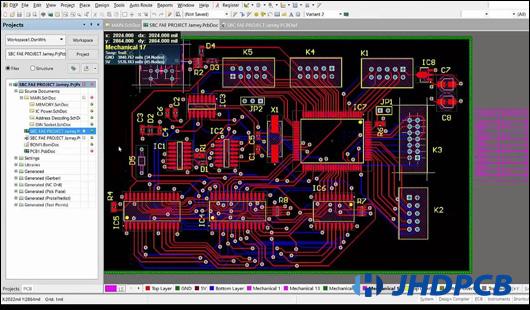
Two: Select the correct grid – pay attention to use grid spacing which can match most reasonable components.
Since many devices come in various of packing sizes, engineers should use the device that best fit for their design. Additionally, polygon is very important for plate copper deposition. Polygon filling deviation usually occurs when polygonal copper is applied to multi grid PCB, which is not as standard as that based on a single grid, but the provided plate life exceeds the requirements. Although multi-grid seems to be a powerful tool, engineers who think more about PCB layout early in design can avoid spacing problems and make full use of circuit boards.
Learn more about PCB design layout information;
Three: Put the relevant components and required testing points together.
Place the discrete components required by the project close to the device so as to keep the bypass capacitor and resistor be in the same position with it, which helps to optimize the circuits length mentioned in rule 2, and also makes testing and inspection easier.
Four: Manage the distribution of power and ground wires by using the power layer.
For most PCB design software, copper clad power layer is a faster and simpler choice. By connecting a big number of conductors together, it can be ensured that the most efficient current can be obtained with the minimum impedance or voltage drop, while providing sufficient grounding loops.Running multiple power lines in the same area of the board to confirm whether the ground aeroplane covers utmost of the PCB, which is conducive to the commerce between conterminous layers, If possible.
Five: Integrate component value.
During the procurement of PCB customized components. Some discrete components make the same performance feature but with higher or lower cost. It is possible to simplify the bill of materials and potentially reduce costs by consolidating within a small range of standard values. It will also help you to make correct inventory management decisions during the long period if you have a series of PCB products based on preferred equipment values.
Six: Design PCB panels.
Selecting the size of the laminates most suitable for the manufacturer’s production will help to reduce prototype design and production costs. First lay out the PCB circuit board on the panel, contact the PCB circuit board manufacturer to find out their preferred size for each panel, then modify your design specifications and try to repeat your design as much as possible within these panel sizes.
Read more PCB panel knowledge;
Seven: Use silkscreen effectively .
Silkscreen always be used as marking some useful information by PCB circuit board producer. Clearly indicate not only the function and test points, but also the orientation of components and connectors as far as possible. Fully applying screen printing technology on the surface of PCB can coordinate the whole PCB production process. We provide detailed PCB silkscreen information and guidance on design considerations. I hope that can give you help.
Eight: Perform as many design rule checks (DRC & DFM) as possible.
Although it takes only a short time to run the DRC function on the PCB software, in more complex design environments it is a good habit to keep in mind that you can save a lot of time as long as you perform checks throughout the design process. Every routing decision is critical, and performing DRC keeps you informed of the most important routings. JHD also provides free DFM file checking to avoid errors while giving the most economical production solution.
Nine: Decoupling capacitor is needed.
Never try to optimize your design by avoiding decoupling power cords and limitations in the dependent component data sheet. You can spend as much time as possible installing them because capacitors are cheap and durable, while following rule 5 and using standard value ranges to keep your inventory clean.
Ten: Generate parameters of PCB manufacturing and verify them before production.
You can first export the Gerber file and use a free viewer to check that if it works as expected to avoid production mistake. Jhdpcb is pleasure to verify for you. Just contact us to send the Gerber file. We will implement strict verification according to the situation and put forward some improvement suggestions to ensure the good quality. Avoid production loss because of wrong parameters.
As circuit design becomes more and more widely shared and special teams increasingly depend on advanced design, the above basic rules will still be an indispensable step in PCB design, which we believe is very important for PCB design. Designers can realize value of their products mostly,and also the maximum benefit from the PCB circuit boards they fabrication,by clarifying these basic rules we talked about.
For more information on PCB project requirements, please feel free to contact us. We will provide you with high-quality PCB with rich experience and first-class precision equipment. Regardless of any type of PCB, PCB assembly, small or high volume needs. We will all take our strengths and ingenuity seriously to help all customers solve their PCB needs.