
Problems:
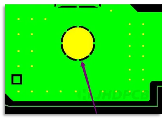
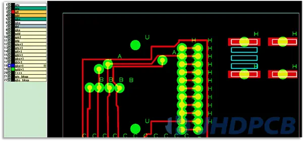
a. As shown in the figure above, the lines corresponding to the vias plate have electrical performance connections, and NPTH are required.
b. As shown in the figure above, the hole plate corresponds to the circuit without electrical performance connection, and requires metal holes.
JHDPCB Suggestion:
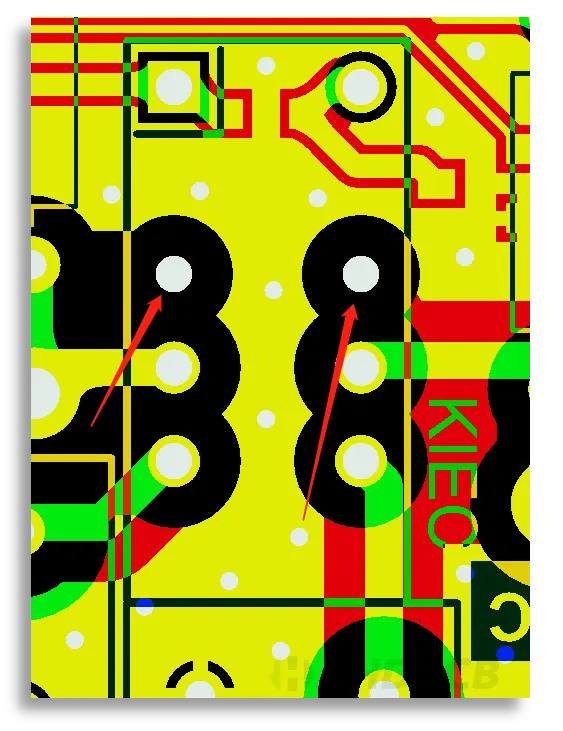
According to the standard design, if a non-metal hole is to be made, make sure that the corresponding circuit has no electrical performance connection, and the plate is the same size as the hole design or has no plate; if a metal hole is to be made, ensure that there is an electrical performance connection, or the plate is larger than the hole on one side about 5mil;
In addition, note that if metal holes are to be made but there is no disk in the corresponding circuit position, the back end must go through the positive electroplating process, and the delivery time will be extended by more than one day compared to the negative process, so this design is not recommended.
Correct design: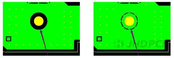
It is best to attach a hole table to clearly mark which are PTH and which are NPTH; it will lead to unnecessary time-consuming EQ communication.
For example: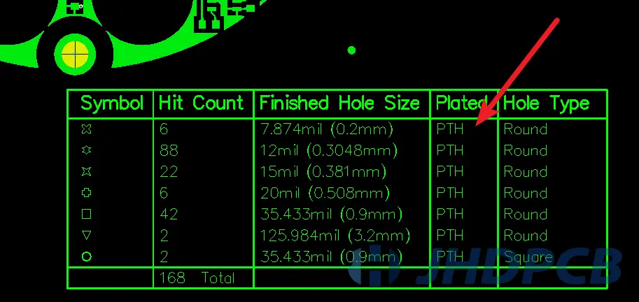
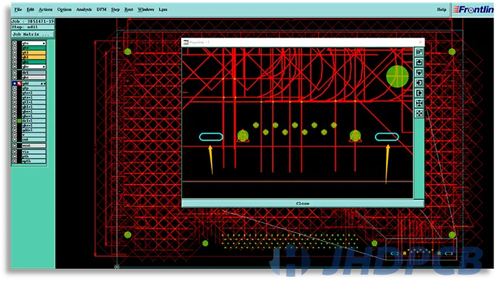
Problems:
There are 7 slots in the above picture. The customer requires that the three red positions in the middle should be made of non-metal slots, and the other four slots should be made of metal slots, but all slots are uniformly designed on the gdd layer. If according to the design, the normal default is to make non-metallic grooves, and the rear end will open the disk to prevent copper exposure during groove milling.
JHDPCB Suggestion:
Separate design, the non-metal slot is placed on the gdd or gm1 layer, the metal slot is placed on the drl layer, or the slot layer is output separately.
correct design: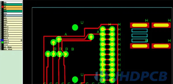
Problems:
1. The hole symbol mark in the pcb design file is too large. When the pcb manufacturers want to check whether the hole and the hole symbol correspond one by one, there is no way to start, therefore the hole position and size deviation caused by the import scale problem cannot be found;
2. The slot is designed in the corner of the hole symbol, and there is not any mark in the hole table, very easy to miss the slot.
JHDPCB Suggestion:
Do not design the hole symbol too big, and it can be clearly seen one by one corresponding to the drilling;
Provide a hole table, mark the position and parameters of the slot, or put it into the through-hole drl layer;
Correct design: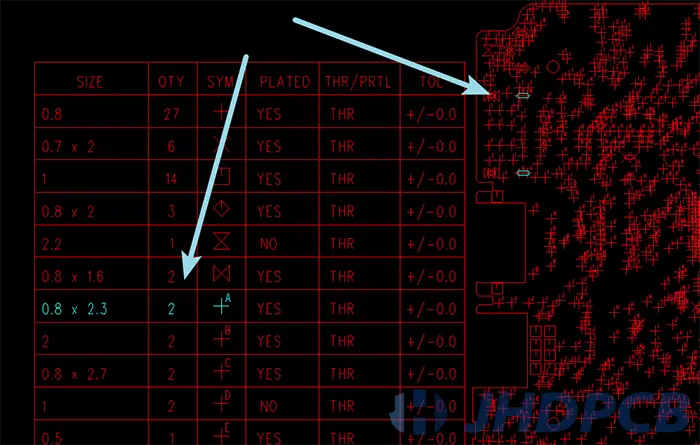
Problems: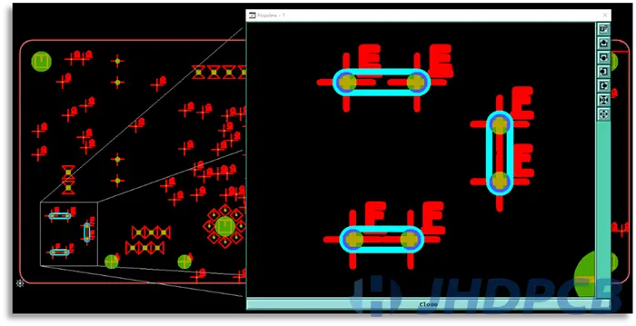
The actual position of the hole design has a slot, the design is unreasonable and there is no additional explanation.
JHDPCB Suggestion:
Do not design holes and slots at the same position; provide a hole table, mark the position and parameters of the slot, and design the corresponding slot directly on the drl layer;
Correct design: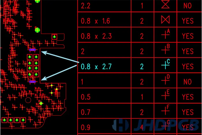
Problems: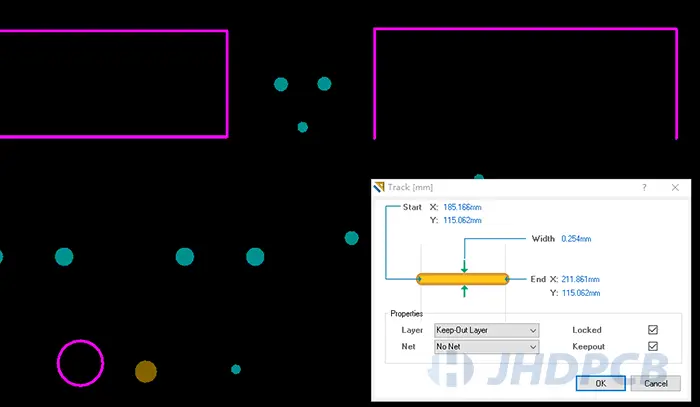
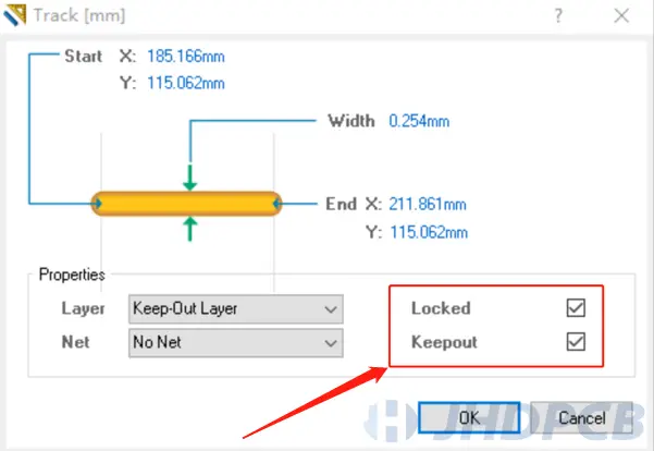
When converting PCB files to geber files, slot locking is easy to miss.
JHDPCB Suggestion:
When designing the PCB files, uncheck the Keepout- tagging option.
Correct design: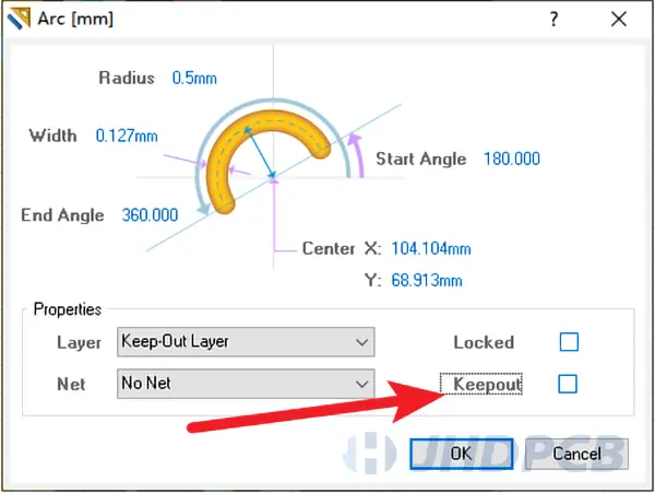
Problem: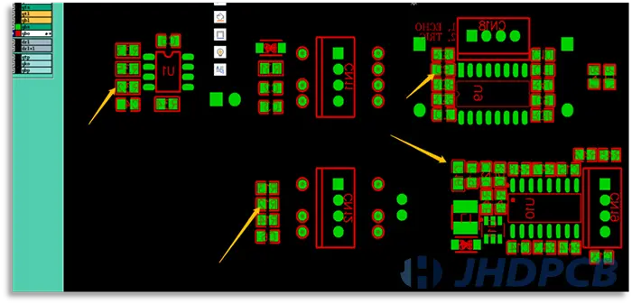
The solder pad is usually mounted by machine, so seems the position of the character is not very important, but from the perspective of the JHDPCB manufacturer, if the character position on the pad, we will judge that the design is abnormal, and will communicate with the customer to change the position of characters or delete characters, which consumes valuable time.
JHDPCB suggestion:
For the convenience of maintenance and welding, the character symbols should be placed outside the frame during design, and the character symbols should be placed in order or not placed in the dense area.
Click for comprehensive PCB character silkscreen information.
Consideration when designing internal milling grooves.
The actual milling cutter can’t go in and the production efficiency problem. Check out our Mechanics article for detailed PCB milling knowledge.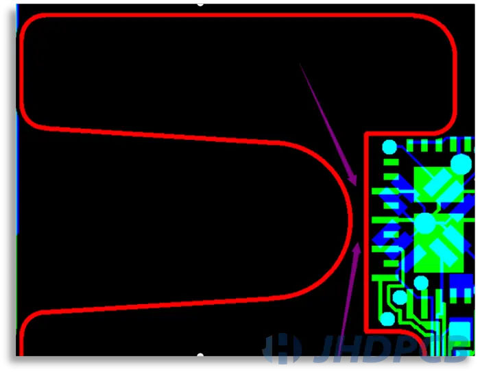
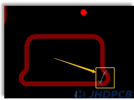
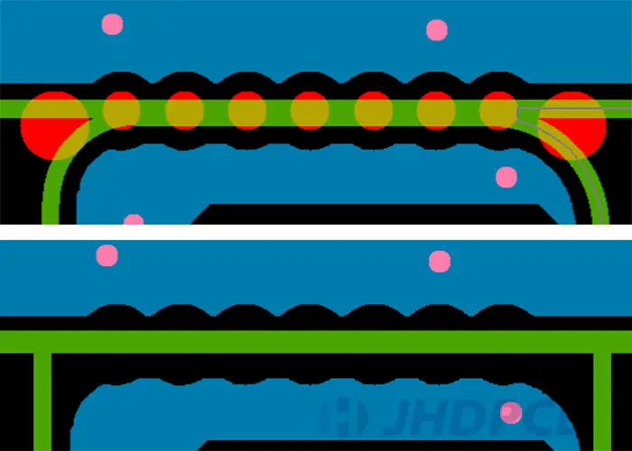
Problem:
In the gerbers provided by the customer, the inner groove needs to be hollowed out, but the distance between the arches is less than 0.8mm, and the conventional milling cutter cannot enter.
JHDPCB suggestion:
If the function of this board is not affected, customers can be advised to increase the distance at the arc; place a “corner hole” at the concave corner (see the white arrow in the figure)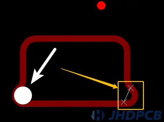
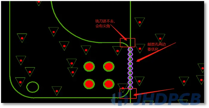
Problem:
When the board edge connection position is designed, two adjacent boards have rounded corners on one side, straight edges on the other, and stamp holes in the middle. When the milling cutter cuts, there will be sharp corners behind the board, which needs to be welded.
JHDPCB suggestion:
without affecting the structure, it is recommended to change the rounded corners to right angles or add “corner holes” to increase production efficiency and make the boards more beautiful.