Mechanics
directory
What is PCB mechanics?
PCB mechanics refers to a general term for all mechanical and physical processes in the PCB manufacturing process, which mainly includes three processes: Milling, V-scoring, and Back drilling.
What information does the pcb mechanical properties contain?
The mechanical and physical process of pcb generally includes drilling, trimming, gong groove, and slot, milling, V-scoring, back drilling. Therefore, PCB mechanical properties include (without limitation) the properties of the above-mentioned mechanical physical production processes.
What is Milling?
Printed circuit board milling (also known as isolation milling) is the process of removing copper areas from a piece of printed circuit board material to recreate pads, signal traces, and structures based on patterns in a digital circuit board plan called a layout file.
The PCB milling process, which is similar to the more common chemical PCB etching process, is a subtraction process: the material is removed to create the required electrical isolation and ground plane. However, unlike chemical etching processes, PCB milling is often a non-chemical etching process and can therefore be done in a typical office or laboratory environment without exposure to harmful chemicals.
In the case of PCB milling, the quality of the circuit board depends primarily on the authenticity of the system, or weighting, milling accuracy and control, and the conditions of the milling drill (sharpness, tempering) and their respective feed/speeds. In contrast, in a chemical etching process, the quality of the circuit board depends on the accuracy and quality of the photomask and the state of the etching chemical. Of course, milling is unlikely to replace etching in mass production, although the use of CNC is already the standard practice for drilling plates.
Milling parameters:
| Parameter | Value |
|---|---|
| Minimum milling tool diameter | 0.8mm |
| Smallest radius for inner corners | 0.4mm |
| Minimum spacing copper / milling contour | 200µm |
Milling application:
| Application | Milling tool diameter Ø | Multi-CB Service |
|---|---|---|
| Standard | ≥ 2.0mm | Inclusive |
| Special | ≥ 0.8mm < 2.0mm | Inclusive |

NPTH slots/Milling - Design parameters:
| Option | Parameter |
|---|---|
| Min. width: | 0.8mm |
| Layer: | Dimension layer, e.g. EAGLE layer 20 |
| Copper clearance: | 150µm |
| Note: | Copper exemption needs to be carried out. |
PTH slots/milling - Design parameters:
| Option | Parameter |
|---|---|
| Min. width: | 0.8mm |
| Layer: | milling (mechanical layer), e.g. EAGLE layer 46 |
| Note: | Needs copper connections on TOP and BOT for through-plating. |
The internal and outside board contours are milled according to per clients’ specifications.
Depending on the customer’s requirements, the outer contour may be 90° and round, but the inner corner is designed to have at least the diameter of the milling cutter. Usually, the edges of the rectangle orbit the earth; Matching milled parts should also be punched on the sides to maintain a precise rectangular area.
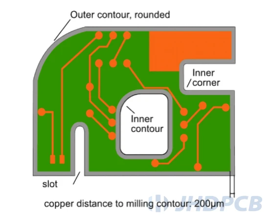
The separation and contouring of PCBs is usually machined. Given that there are certain rules:
- Usually, there is no additional frying price.
- With the copper endurance of the circuit board, the danger of harm must be avoided.
- The inner and outer contours of the plate should be marked with a channel length of 1μm to avoid measurement and dimensional issues.
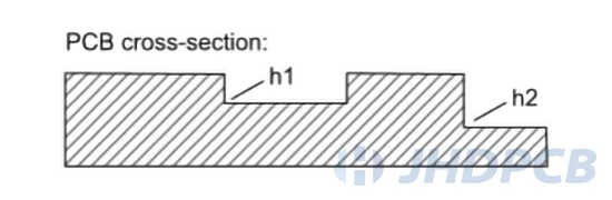
Z-axis milling (level milling):
Z-axis milling refers to the milling of a variable horizontal height that can be milled at edges or within a circuit board.
Create a new layer in the PCB design software for Z-axis milling only. Set the profile of the milling area (1 mil) and note the desired milling depth (tolerance ±0.20mm).
The Z Axis Milling option in pcb calculator is now activated.
PCB milling advantages:
There are some advantages of PCB milling for both prototyping and some special PCB designs. The biggest benefit is that there is no need to use chemicals to produce PCBs. Outsourcing a board takes time when creating a prototype. Alternative is to make a PCB in-house. With the wet process, there are some problems with chemicals and disposing with in-house production. High-resolution circuit boards using the wet process are difficult to achieve and still, when done, one still has to drill and eventually cut out the PCB from the substrate. CNC machine prototyping can offer a fast-turnaround circuit board production process without the need for wet processing. If a CNC machine is already used for drilling, this single machine could perform both drilling and milling at the same time. The CNC machine is used for drilling, milling and cutting. Without the use of top-of-the-line systems that typically cost several times more than CNC milling machines, many easy-to-mill circuit boards will be difficult to machine in a laboratory environment by wet etching and manual drilling. In large-scale production, although the use of CNC is already standard practice for drilled boards, milling is unlikely to replace etching.
What are the effects of reasonable PCB milling on PCB appearance production? Learn from our historical experience.
What is V-scoring?
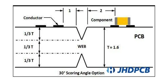
PCB V-Scoring is the process of cutting a “V” shaped groove at the top and bottom of a printed circuit board (PCB). V-scoring not only does it keep the board intact while splitting it, but it also makes it easier to remove discrete parts from the board. Only a little material is needed to hold the two parts together.
The Process of V-Scoring:The V-scoring process consists of two blades at any angle, such as 30o, 45o and 60o bevels. The blade is like a wheel with many gears, and the gear is the knife used to score. One blade is at the top and the other at the bottom, and they rotate point-to-point, requiring a certain distance for the PCB board to pass through. The distance determines the remaining thickness in the middle of the two Vees. The remaining thickness supports PCB units that hold sub-plates (/set) or production panels together. After PCB board assembly process, the sub-panels will be divided into separate PCB assemblies.
Basic rules of PCB V-Scoring:
- The board spacing is 0mm;
- The minimum milling slot width between the circuit board and the process edge is ≥1.6mm;
- The V-splitting line must be straight, vertical and horizontal;
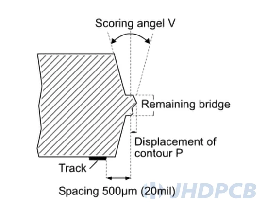
- The distance between the V-shaped engraved line and the contour is maintained at 0.35mm;
- The minimum PCB size of V-scoring is 75 x 75mm, and the maximum size is 450x1245mm;
- The default minimum inner angle ≥ 0.8mm, if there are special requirements, it needs to be marked;
- The outer angle is ≥ 1.0 mm, if there are special requirements, it needs to be marked;
- Note that the V-shaped scoring angle is 30 degrees;
- Knife jumping distance: 8 mm;
V-Scoring parameters:
| Option | Parameter |
|---|---|
| Remaining bridge thickness | approx. 0.3mm |
| Scoring angle | 30° |
| Minimum copper/scoring line spacing | 500µm |
| Edge displacement P* | +/- 150µm |
V-scoring advantages:
PCB V-scoring is the primary source of cost advantages for electronics manufacturers. It eliminates the need for space required for routing, thus providing the ability to add more rows to the manufacturing panel. This eliminates wasteful laminates. V-scoring not only saves money, but also time because it simplifies manufacturing and processing methods.
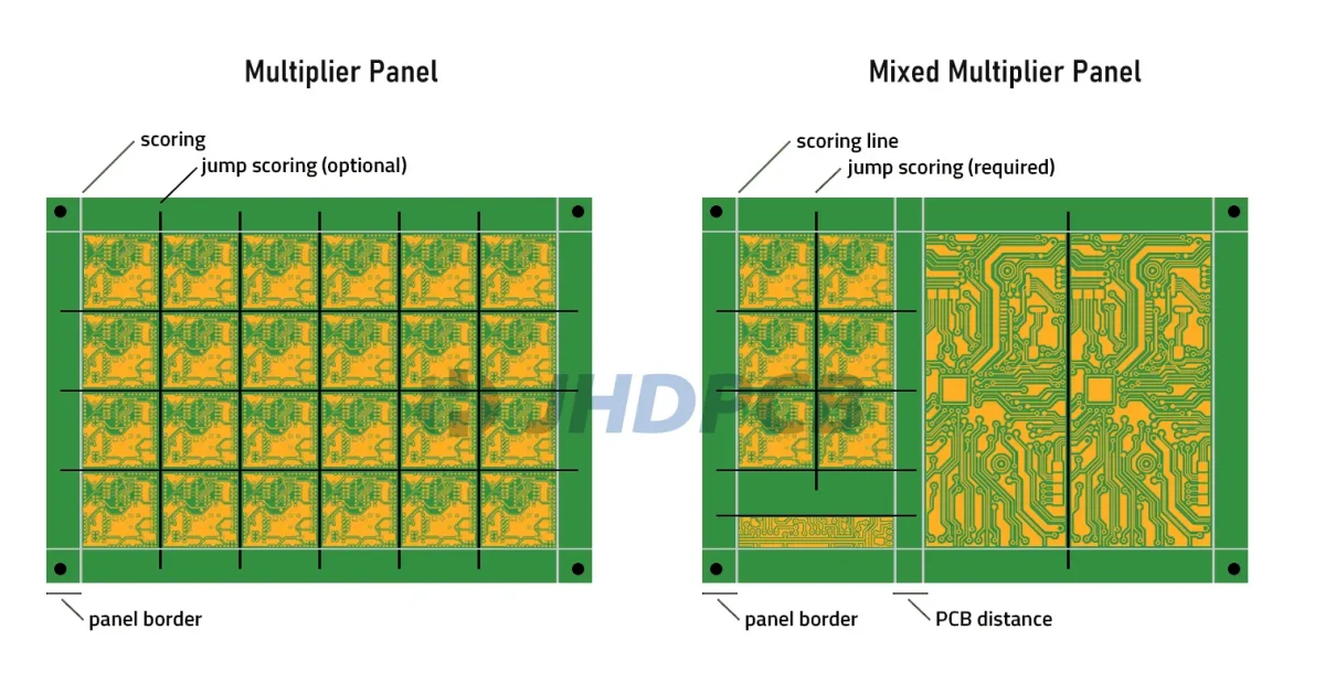
PCB jump scoring:
In some cases, you do not want the V-score to pass through the PCB rails of the array. When you have heavier components or thin laminates, you may need the waste rails to keep the strength of the array so that the individual parts do not fall apart until they are assembled. In this case, you need to lift the blade from the laminate surface before reaching the end of the panel. Because the blade needs to “skip” certain parts of the array, it is called PCB Jump-scoring.
For example, for a more stable panel border (optional) or for scoring in a hybrid multiplier panel (different circuit board images).
e.g. Multiplier Panel: (jump scoring optional)
The entry and exit path of the scoring blade is 15mm, each.
The circumferential panel border should therefore be min. 15mm, better 20mm.
e.g. Mixed Multiplier Panel: (jump scoring required)
The entry and exit path of the scoring blade is 15mm, each.
The circumferential panel border should therefore be min. 15mm, better 20mm.
The distance to the neighboring PCB (in extension of the score line) should therefore be min. 15mm, better 20mm.
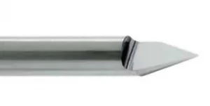
CNC scoring of any shape:
V groove cutter for CNC-scoring–
If your application requires it, you can score any shape, such as a star, radius, and so on. Classic scoring is much faster to process than milling, while CNC scoring are much slower. As a result, CNC scoring is more time-consuming and costly.
Therefore, if possible, you should choose milling instead of CNC scoring. Also note that non-rectangular shapes can make manual breakouts more difficult or require assisted scoring.
CNC scoring are done on a “normal” milling machines for PCBs using V-slot milling cutters.
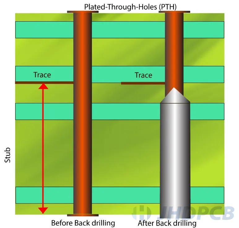
what is backdrill ?
Back drilling or Controlled Depth Drilling (CDD) is a technique used to remove the unused portion, or stub, of copper barrel from a thru-hole in a printed circuit board. When a high-speed signal travels between PCB layers through a copper barrel, it can be distorted. If the signal layer usage results in a stub being present, and the stub is long, then that distortion can become significant.
These stubs can be removed by re-drilling with a slightly larger drill bit after the fabrication is complete. Drill the hole back into a controlled depth, approaching but not touching the last layer used by the through hole. Given the changes in fabrication and materials, a good fabrication can drill back to leave a 7mil stub, ideally the remaining stub would be less than 10mil.
(The images presented below illustrate the steps involved in CDD involving reducing signal reflection due to through-hole stubs.)
Advantages of Backdrill:
- Increase data rate;
- Reduce deterministic jitter;
- Reduce signal attenuation through improved impedance matching;
- Minimal design and layout impact;
- Lower bit error rate (BER);
- Increase channel bandwidth;
- Reduce EMI/EMC radiation from the tip;
- Reduce the excitation of resonance modes;
- Reduce crosstalk between vias;
- Cost is lower than sequential lamination
Backdrill Design Parameters:
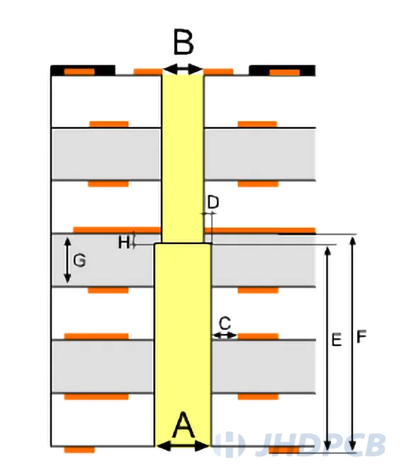
| Index | Type | Value min |
|---|---|---|
| A | Backdrill Ø | 400µm |
| B | Plated-through via Ø | 200µm |
| C | Copper clearance | 150µm |
| D | Ø-Difference circumf | 100µm |
| E | Backdrill depth | 200µm |
| F | Distance to connected layer | see below |
| G | Thickness target layer | see below |
| H | Thickness stub remainder (safety) | see below |
The basic characteristics of back drilling:
- The back is mostly hard board;
- Board thickness exceeds 2.5mm;
- Usually used for 8 floors or above;
- The back drill is 0.2 mm larger than the through hole;
- Back drilling depth tolerance +/-0.05MM;
- The minimum clamping size is 0.3 mm;
JHDPCB is one of the leading PCB manufacturers in China. We have over 10 years of experience in providing innovative PCB manufacturing services using modern technology and the latest machinery. We adhere to strict high quality standards to produce products. We can meet the various needs of our customers, from simple circuit boards to the most complex circuit boards. We are able to provide better service and convenience to our customers. For more PCB information, you can contact us through live chat or email on the website, or you can call us (+86 755 2753 9533).


