Why choose JHDPCB?

  • Real PCB and PCBA manufacturers;
  • Meet industry certification and production standards;
  • 99% delivery on time;
  • 10+ years of industry experience;
  • 150+ experienced R&D team;
  • 5000+ orders/day;

contact us

Provide quality service for your PCB project. Tel: +86 755 2753 9533

$50

Welcome Coupon

Available for orders over $100.
This coupon can only be used by new JHDPCB customers.

PCB Layout Design

directory

What is PCB layout?

PCB layout meaning is based on signal quality, EMC, thermal design, DFM, DFT, structure, safety requirements, etc. PCB layout design is the first important design aspect of the entire PCB layout process. The more complex the PCB is, the better the layout is, because it directly affects the ease of assembly of the subsequent wiring. The PCB board layout should meet the following requirements: shortest possible overall connection, shortest possible key signal lines, complete separation of high-voltage and high-current signals from low-voltage, low-current and low-current signals, separation of analogue and digital signals, separation of high-frequency and low-frequency signals, high-frequency components at a good distance. Local adjustments should be made to meet simulation and timing analysis requirements.

PCB design is one of the most important design elements in electronic product design. Printed circuit board (PCB) design is not easy. It is a key part of electronic product design, including PCB routing and component placement layout. The performance of a circuit depends to a large extent on its layout on the PCB, so it is important to learn more about PCB design and layout techniques. A good PCB design can greatly reduce the cost of the board and minimize the risk of errors in the PCB manufacturing process.

PCB Design-2

What's the Importance of a PCB layout?

When it comes to printed circuit boards, the design layout is the most important part as it determines the positioning of the various components and their final role in the desired product. In addition, In order to finished perfect PCB layout we should learn more about PCB layout tips and PCB layout considerations.
In some PCB design teams, the project is handed over to an experienced technical person who uses best practices and avoids known placement considerations. In most cases, advanced CAD software is used to maximize efficiency, identify potential design problems and point out obvious errors. Layout is an important part of circuit board design and an essential component of electronic products. A correct layout is the first step to a successful PCB design, as a good layout directly influences routing.
The importance of layout has the following points:

  • A good layout determines the wiring density, and the number of wires passing through the holes, and thus influences the signal quality.
  • A good layout reduces processing costs and facilitates subsequent SMT/manual soldering.

What are the prerequisites for PCB layout design?

  • Schematic diagram (.DSN and .SCH suffix).
  • DXF structure drawing.
  • Component specifications.
  • Special requirement.

Schematic diagram (.DSN and .SCH suffix).
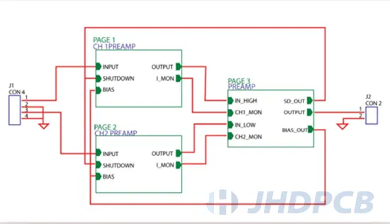
A PCB design schematic can be described as a circuit diagram or functional diagram of an electronic circuit. Symbols can be used to represent the components and it can show how they are electrically connected. This graphic representation of the electronic circuit is created before the actual circuit layout. The circuit layout must include the arrangement of the basic components, the traces and the connection diagrams for each layer. When designing a PCB layout, it is always important to start with a circuit diagram to help build and understand the circuit system.

Schematic diagram

DXF structural drawings.
DXF is a 2D drawing in AutoCAD format used for positioning equipment and creating panel dimensions.

Component specifications.
Specifications should be created at the same time as the equipment sizing diagrams and packaged so that they correspond exactly to the physical object.

Special requirements.
Characteristic impedance: Characteristic impedance refers to the process of resistance propagation of high-frequency signals and electromagnetic waves up to a certain frequency, signal transmission line and reference layer.
The PCB of electronic products not only plays the role of power line, but also plays the role of signal transmission; the circuit performance of electronic products, high frequency, high speed, PCB must be provided to ensure that the signal does not reflect in the transmission line, to maintain signal integrity without distortion. Characteristic impedance is at the heart of solving signal integrity problems.
High frequency:High-frequency PCBs, whether rigid or flexible, enable higher signal speeds and frequency bands of up to 100 GHz. Crucially, there are a number of materials designed for use in the high-frequency range: RF PCBs are characterized by low dielectric constant (Dk), low dielectric loss factor (Df) and low coefficient of thermal expansion; they are regularly used in HDI technology; they are also used in the manufacture of high-frequency devices such as mobile phones and cellular phones; they are also used in the manufacture of high-frequency devices such as mobile phones and cellular phones. They are also widely used in high-speed communications, telecommunications and RF microwave technology.

How to read PCB layout?

Reading layout PCB is a set of rules for placing electronic components on a printed circuit board. When designing electronic circuits on printed circuit boards, it is important to have a clear plan and detailed instructions on what can and cannot be done before starting the PCB layout.
Understanding the circuit is very important in design, for example knowing the maximum current and voltage that can flow through the circuit for each conductor. Once these values are known, it becomes easier to determine the conductor width and the type of PCB to be used.

The voltage difference between individual traces determines the required distance between individual conductors. If the distance is not sufficient, there is a risk of sparks or shorts on the PCB due to the potential between the individual traces. It is therefore very important to consider some of these basic requirements before proceeding with PCB design.
Ignoring important aspects during PCB design and layout services of electronic component layout can result in a design that does not work well. Improper wiring can lead to problems such as EMI, component conflicts on both sides of the PCB, limited circuit functionality and even circuit failure.
In addition, if the wiring is not done right the first time, it may have to be redone, resulting in production delays and additional costs.

PCB Design

PCB Design Layout Rules and Precautions.

As mentioned earlier, many PCB designers use a list of guidelines for component placement and routing. Now that we know a little more about noise sources, antennas and coupling mechanisms on PCBs, we can take a closer look at some of these PCB layout guidelines and understand why and when they are important. Effective PCB design skills can improve the practicality of PCB layout design and reduce unnecessary troubles.

Overall PCB layout:
At the beginning of PCB design, it is best to make a preliminary plan for important components and circuits to facilitate the determination of the circuit board area and the number of wiring layers.
The length of tracks carrying high-speed digital signals or clocks must be kept to a minimum.
High-speed digital signals and clocks are often the strongest sources of noise. The longer these traces are, the more chance there is of energy coupling outside them. Also remember that the loop area is generally more important than the length of the track. Make sure that there is a good high-frequency current return path close to each track.
The length of tracks directly connected to the connectors (I/O tracks) should be kept to a minimum.
Traces directly connected to the connectors are likely to be energy-coupling paths to or from the PCB.
High frequency signals must not be routed under components used for I/O on the PCB.
Tracks routed under a component may capacitively or inductively couple energy to the component.
All connectors must be placed on an edge or corner of the board.
Connectors are the most efficient antenna components in most designs. If they are located on the same board edge, it is much easier to control the common-mode voltage driving one connector than the other.
There should be no high-speed circuitry between the I/O connectors.
Even if two connectors are on the same board edge, high-speed circuits can induce sufficient common-mode voltage between them to drive one connector over the other, resulting in significant radiated emissions.
Critical signal or clock lines must be laid between the supply and ground planes.
Laying the track in a layer between two fixed planes is a good way to contain the fields of these tracks and prevent unwanted communication.
Select active digital components with acceptable maximum off-chip transition times.
If the transition time of the digital waveform is faster than necessary, the power of the upper harmonics may be much higher than necessary. If the transition time of the logic used is faster than necessary, it can usually be slowed down by the use of series resistors or ferrites.
All external communications from the same device must be routed through the same connector.
Many components (especially large VLSI devices) generate significant common-mode noise between I/O pins. If one of these devices is connected to one I/O pin, the device may be connected to another. If one of these devices is connected to more than one port, this common mode noise can affect the good antenna (the device will also be more susceptible to noise emanating from that antenna.)
High-speed (or sensitive) traces should be routed at least 2X from the edge of the PCB, where X is the distance between the trace and its current return conductor.
Electric and magnetic field lines connected to traces in close proximity to the edge of the PCB are considered to a lesser degree. Crosstalk and coupling to and from the antennas is generally higher with these traces.
Pairs of differential signal lines should be routed together and have the same distance to each fixed plane.
Differential signals are less susceptible to interference and produce fewer emissions if they are symmetrical (i.e. have equal length and impedance to other conductors).
Copper trace:
The copper traces should be neat and smooth. And you will find that in professional PCB design, most of the copper traces on the PCB are bent at a 45° angle. The reason is that the 45° angle shortens the electrical path between the components compared to the 90° angle. For high-speed circuits, it is best to avoid a 90° angle.
Ground wire and power wire:
Some key copper wires, such as ground wires and power wires, should be as thick as possible to improve anti-interference ability and power efficiency.
See “10 Golden Rules of PCB Design” for more basic best rules for PCB design.

The PCB layout design steps.

In this PCB layout tutorial, This section presents the steps of PCB layout and design:

  • Create a PCB schematic Diagram.
  • BOM validation.
  • Pre-Layout stage.
  • Generate the production files.

PCB-design-layout-3

A schematic is an abstract, graphical, symbolic representation of the elements of a system. At this stage, the design is entered into a schematic tool (e.g. Altium, Allegro). The schematic shows the components used in the design and how they are connected.

  • Generation of schematic symbols:
    The Altium Designer symbol generation tool is accessed through the Tools → Symbol Wizard option in the main menu. The symbol generation process consists of drawing the part body, adding pins and pin numbers, defining reference designators and assigning footprints.
  • Symbol connections:
    For PCB designers, it is very important to clearly show the connections between components on the circuit diagram: where two wires cross and are electrically connected in common, there must be an intersection point. This is a common practice in any circuit design.
  • Associating tracks and symbols:
    When transferring schematic information to the PCB layout, the component floor plans are displayed on the schematic.
  • Generating netlists:
    The netlist of any PCB design software contains information about the component pads to be connected as well as the component designation. The netlist also assigns serial numbers to the connections. The Netlist Manager dialogue box is used to control and manage the PCB’s netlist. Nets can be edited, added or deleted as required. Component pins (or pads) on nets can also be edited.
  • Performing Netlist Checks:
    The Export Netlist option is used to export the PCB netlist to the current document. When the command is enabled, a netlist document with the extension ‘.Net’ is saved in the same folder where the PCB layout document was saved. You must check each net on the schematic (whether all nets are connected as intended).
  • Creating a Bill of Materials (BOM)
    A Bill of Materials (BOM) is, simply put, a list of materials needed to make a PCB. In Altium Designer, a BOM can be generated from the PCB schematic by selecting Report → BOM options.

It is always recommended to briefly review the simple PCB layout after each step/sub-step to ensure an error-free design. For more comprehensive PCB schematic knowledge, please refer to our corresponding blog.

A BOM is simply a list of materials needed to create a PCB. In the pre-design phase, the first step is to check that all the necessary materials are available for the design.
The stacking is designed using the CM (contract manufacturer). Designers need the details of the stack before they can start designing the layout. The design of the stacking is always done by the designer, but usually the manufacturer is assisted by a manufacturing company to find a suitable stacking layout.

  • Stack layout.
    Set up stack-up and design rules and start with the PCB layout. The stack-up is set up on the tool with the layer layout manager; the stack-up is set up in the layout tool with the stack-up plan generated by the PCB manufacturer’s stack-up tool as a reference.
  • Set up PCB design rules.
    PCB layout design rules are a set of guidelines for PCB layout tools to follow; PCB constraint settings cover all aspects of the design. PCB design rules can be divided into three main categories.
  • Drawing the PCB outline.
    The shape of the PCB is called the PCB outline and is essentially a closed contour; the shape of the PCB can be redefined in a number of ways.
  • Placement of components.
    The first step in component placement is to divide the layout according to the function of the circuit (analogue, digital, high speed, high current, power, etc.)
  • Routing the network on the PCB.
    Routing is the process of laying copper wires between nodes. This conductive path is defined by the placement of traces, arcs and vias in the copper layer, creating a connection between two nodes.
  • Performing Design Rule Checking (DRC)
    Design Rule Checking (DRC) is the process of checking the logical and physical integrity of a design. DRC checks all design rules used on the PCB. This function can be implemented in a network so that the checks can be performed in parallel with the design progress. This step should be performed on every PCB that is routed to ensure that the minimum design rules are met and not violated.

    Design rule check dialog

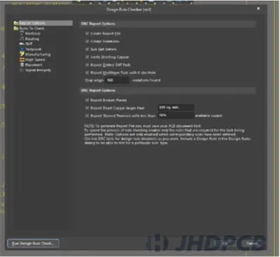
  • Complete PCB manufacturing/assembly notes.
    The PCB construction note contains the following information about the design.
    1. PCB class (Class 1/Class 2/Class 3).
    2. number of layers.
    3. total thickness of the PCB.
    4. IPC standards to be met (e.g. IPC-2221).
    5. color of the welding mask
    6. color of the silkscreen
    7. impedance details of each layer
    8. cut-out details
    9. stacking details
    10. drilling details (drilling plan)
    11. number and date of issue
  • Creating Gerber and other production files.
  • Performing a DFM check.

These are the PCB layout basic steps for laying out a PCB.

How to make pcb layout from circuit diagram?

The procedure for converting a schematic to a PCB layout is a simple three-step process.

  • Step 1: Prepare for design synchronization.
    Ensure that the schematic does not violate any design rules that would prevent synchronization with the PCB schematic;once the PCB schematic is created, this first synchronization step ensures that subsequent changes to the electrical schematics are immediately imported into the PCB schematic.
  • Step 2: Import the design data into the PCB using the schematic entry tool.
    Import the PCB into an empty PCB schematic using the Schematic Capture tool. A new PCB file must be created in the current project and the component footprints must be imported into the new PCB using the Schematic Capture tool.
  • Step 3: Define the layer stack.
    Define the layer stack for the new PCB. Once these three steps are completed, it is time to start placing the components and tracks together.

What are the common problems with PCB layout export?

The printed circuit board (PCB) is an essential component of electronic products. Yet designing a PCB is never a simple task and many associations, between layers, components or circuits, must be handled properly. A poorly thought-out design can lead to errors or even disasters when used in an electronic system. Despite the difficulty of PCB design itself, some of the common problems can be summarized so that all PCB designers can learn about them in advance and how to deal with them before the PCB manufacturing stage.

Missing opening list:
Your Gerber files tell your PCB fabricator what to do and where.  The opening list tells which tool to use.  A single complete opening list for all layers should be sent with your Gerber files for your PCB layout, rather than a separate opening list for each layer.  The opening list is only required if you do not export the Gerber file in 274X format.  The common extensions of this file are .rep, .apt and .apr.
Excellon drill file missing:
Excellon drill files are used in PCB manufacturing to determine how large the holes need to be in your PCB layout and where they should be drilled.  Both plated and unplated holes must be included in a drill file.  Plated and unplated holes will have different tool numbers.
Missing tool list:
A tool list must be embedded in your Excellon drill file or sent as a separate text file.
Ring-shaped ring insufficient:
An annular ring is the “donut” (ring) that is created when your drill pierces a copper layer.  It is defined as the radius of this ring.  For example, a 0.030″ dowel with a 0.020″ hole has a 0.005″ ring. This ring is necessary to allow full plating of vias as well as solderability of component holes. Often the requirements for the ring are not observed.
Insufficient width/spacing of copper tracks:
Copper trace spacing is the minimum air gap between two adjacent copper elements. The trace width is the minimum width of a copper element, usually the traces.
Insufficient internal spacing:
The inner air gap is the minimum distance between the edge of a hole and any adjacent unconnected inner layer copper. Adequate internal clearances ensure that your drill will not cause shorts in your inner copper layers. This is important for both plated and unplated holes, as unplated holes can either cut through an adjacent trace or cause a short during assembly.

PCB-layout

What are the common PCB layout software?

In order to create a good PCB layout design, engineers need proper PCB design software to lay out circuits. Engineers use the software to collaborate in the design process, retrieve previously used PCB component designs from PCB libraries, review schematic designs, etc. PCB design software is mostly used as part of other design software systems, such as product and machine design software and general-purpose CAD software. PCB design software is often used as part of other design software systems, such as product and machine design software and general purpose CAD software. Appropriate design software is essential for PCB design, and you should consider whether the software can meet your needs. Here we would like to introduce some of the common PCB layout software.

  • Altium.
  • Altium 365.
  • Fusion 360.
  • Ansys Re Hawk.
  • NI Multisim.
  • Autodesk EAGLE.
  • KiCad EDA.
  • EasyEDA.

How to check PCB layout?

Mistakes are made when designing PCBs; performing a PCB design analysis can help identify and correct these mistakes. This process involves analyzing and improving PCB elements such as stacking, traces, wiring and components to reduce the number of wiring errors to zero. In this part of the report, the inspection and cleaning process is described in detail.

Design and placement of stacking areas:
Placement of the ground, signal and power layers is critical to creating an accurately functioning circuit.
Checking the dimensions of the board:
When installing a PCB in an enclosure, make sure that the dimensions are correct.
Make sure there is an optimum clearance of at least 10 mils between the copper track and the edge of the PCB.
All unplated holes, including mounting holes (minimum hole diameter 3.3 mm), must have an anti-corrosion coating. Screw heads and nuts must be larger than the diameter of the hole.
Placement of the polygonal structure:
Polygons (copper grommets) are filled with copper around the component or trace. They are created only on the signal plane.
When analyzing the PCB design, make sure that there are no floating copper tubes in the circuit. If they are present, connect them to the base plate. Also make sure that they do not create open nets. If necessary, place polygons on other layers to balance the distribution of copper in the stack.
Check the placement of the traces in the PCB design:
Calculate the impedance and current carrying capacity of the traces and optimize the width accordingly.
The length of signal lines and return paths should be kept to a minimum to reduce noise and improve signal integrity.
Recommendations for size and placement:
Drilling small holes is an expensive and time-consuming task. Therefore, the site size should be reduced only when necessary and kept constant. The following drilling parameters should be checked as part of the design review.
Ensure that all bore values are correct and in whole numbers.
Update the designations of through holes, cased and uncased holes in the drilling plan.
Drilling holes and gaps in the solder mask:
When designing the PCB, ensure that all required holes are present in the solder mask layer.
Make sure that the joints and components are not too close together to avoid chipping.
Complete and legible screen printing:
When cleaning the layout, check that the screen print layer is legible and that the letters/digits/symbols do not overlap. A minimum letter height of 25 mils and a line width of 4 mils is recommended. If the print is on the lining or over an opening, it should be offset. The legend should contain all relevant information, such as:

  • Product information: e.g. company logo, copyright notice, warning/hazard label.
  • Component information: Name, orientation, pin designation, first IC contact identification.

Alignment and spacing of components:
Check component alignment and spacing to ensure that components do not overlap.
Traces should not run under or between sensitive elements such as QFP/QFN, POP, BGA, etc.
Design analysis for PCB testing:
Test methods should be selected according to the PCB layout and test pins prepared accordingly. However, the installation of test points can be cumbersome, especially for high-density PCBs. They must be adjusted so that they do not interfere with the actual circuit. For example, the test pins should not be poked over or cause impedance mismatches in high-speed wiring.

What information should the PCB design layout contain when delivered?

Before delivery to the manufacturer, a Design Rule Check (DRC) must be performed to verify the PCB layout design; once the PCB is approved, the deliverables can be released by the manufacturer.
Once the PCB has passed the final DRC check, a design file must be created for the manufacturer. The design file must contain all the information and data required to manufacture the PCB. It also includes notes and special requirements so that the manufacturer knows exactly what your needs are. The following are the files that need to be created:

1. Manufacturing files such as Gerber.

  • TOP – Top copper layer (extension: board.gtl) Specifies the copper trace for the top layer of the PCB.
  • SMT – Top layer of solder mask (extension: board.gts) The solder mask is used to prevent oxidation and the formation of solder bridges during the soldering process.
  • SPT – top layer of solder paste (extension: board.gtp). Solder paste is used to bond surface mount components to pads on printed circuit boards. The paste is applied by nozzle, stencil printing or syringe.
  • SST – Silkscreen Topcoat (extension: board.gto). Silkscreen is a layer of paint used to mark components, brands, logos, etc.
  • BOT – Bottom layer of copper (extension: board.gbl). Marks the copper traces on the underside of the board.
  • SMB – Solder Mask Bottom Layer (extension: board.gbs).
  • SPB – Solder Paste Bottom Layer (extension: board.gbp).
  • SSB – Silk Screen Bottom (extension: board.ghbo).
  • Inner layer for signals and currents.

2. NC drill file: orientation of the drill holes on the board (extension: board.txt).
3. File for selection and placement.
4. IPC 356 netlist file.
5. The ODB++ file (opens database). Information exchange between the design phase and the manufacturing phase.
6. PDF file with schematics and layout.
7. PDF file with assembly drawings.

When your design is complete, your fabrication files must be sent to DFM for review and quotation before proceeding to fabrication and assembly. JHDPCB will provide free PCB file checks to ensure that these file designs are within the capabilities of our production process. Our engineers use more specialized CAM software to do this, and JHD will check your manufacturing files for clearances, feature sizes, material property requirements, feature spacing, surface plating standards, conductor thicknesses, component placement, dimensional and tolerance rules, and more. Whether it is single and double-sided PCB, multi-layer PCB, flexible PCB or HDI PCB, we will strictly review. Make sure the board is ready for full manufacture and use.

Manufacturing instructions are also important as they provide all the other information used to manufacture the PCB. Things like the specific material to be used (CTI600 laminate, high breakdown voltage, etc.), conformal coating, surface finish, impedance requirements, your stackup/material specifications, etc. are specified in the PCB fabrication drawing. Complete and clear manufacturing instructions will help ensure that this PCB design can be produced anywhere.

Feel free to contact us with your needs and suggestions at any time. We will use our strengths and ingenuity to provide high-quality PCB manufacturing and assembly. PCB layout design is a two-way communication process. Effective communication between you and us is the key to the success of the project. Whether it is individual specific needs such as bare board, PCBA or PCB power design, we will use our expertise and personnel equipment to help facilitate better results. 

Get a PCB Quote Now

Open high-quality PCB manufacturing services in JHDPCB