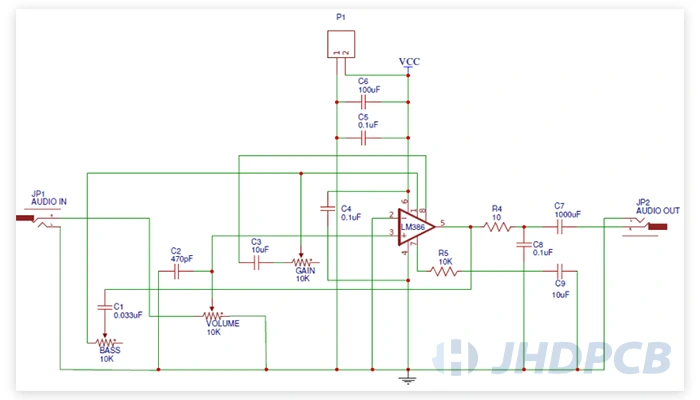

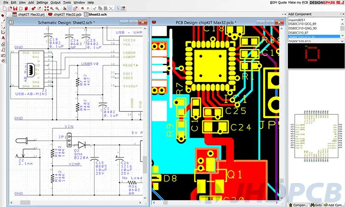
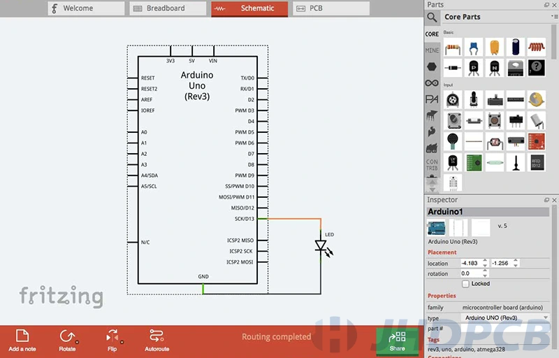
A PCB or circuit board schematic may be a drawing that characterizes the coherent associations between components on a circuit board, whether unbending or adaptable. It essentially appears how the components are associated electrically. The schematic contains a netlist, a simple data structure that records each connection within the design as it occurred within the drawing.
In differentiation. The PCB schematic diagram is a blueprint in the early stage, which mainly shows the key parts of the PCB to realize the connection and constitute the function. Considerations and component locations for the pcb manufacturing process are not included.
The PCB design is very complete when it contains information, following the circuit routing rules, holes, and proper placement of various components. a PCB layout shows precisely where each component is and the wires that connect them.
To draw an effective schematic design, take the taking after standard schematic rules.
- Page size option:
Most design tools offer distinctive page sizes. The designer might select it based on the estimate of their circuit plan. - Page naming agreement:
The logical blocks of the schematic are page-separated. We place pages by placing them alphabetically. To save time, most designers often ignore block charts and revise the history. However, they are accommodating to other designers who try to understand the schematic diagrams. Most of the organizations involved adhering to all of these conventions and directions. - Grid Settings:
Although this is not an immediate requirement from the designers, the tool requires some reference. Having a grid helps designers correctly reference parts and connect. Circuit components must be continuously on the grid and allow network probing during the inspection. - Page title bar:
The page title bar is located in the footer of the schematic page and fills in all the specified details. (Page size, date of update, revision, record number, name/function of circuit, and company disclaimer). - Comments:
Designers need to write the necessary notes about the circuit. You can write messages on standalone documents or schematic drawing pages. Often, for complex designs, annotations are provided on separate pages. Some comments include jumper states and PCB layout constraints/guides.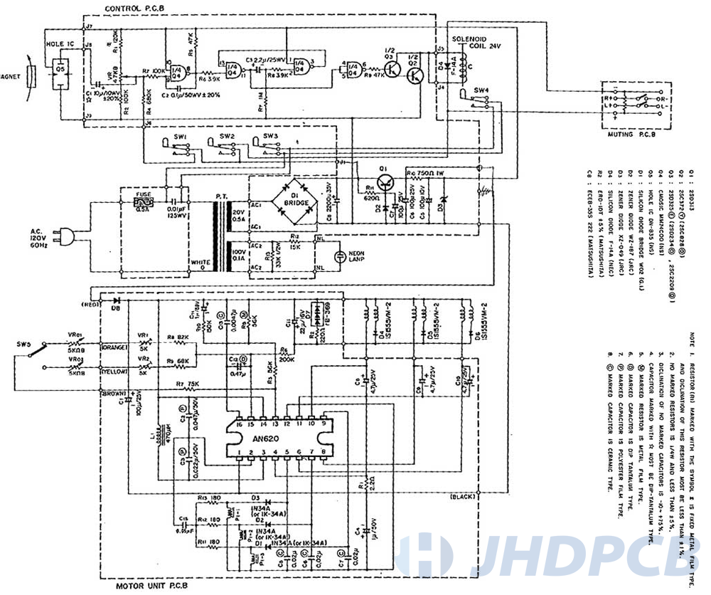
- Revised history:
Revision history records changes made in the design. The document provides information about the date, a description of the changes made, the names of the author and reviewers, and the review comments. The revision history is often set on the primary or final page of the schematic layout. - Schematic document directory:
The directory lists the topics that exist in the schematic documentation. This page helps designers easily find specific modules in a complex design. You can skip this operation if it is small and simple in design. - Block diagram:
Block diagrams speak to diverse modules within the plan and flag flow, dramatically helping reviewers understand the design for a review.
- Layered schematic diagram design:
If the pcb stackup design is complex and contains numerous modules, it is best to have a layered structure. The hierarchy diagram clearly shows that flags flow from one module to another. Click on one of the modules to get a detailed view of that module. - Component reference:
The following table shows the names of the standard electronic components and the corresponding reference indicators used in any schematic diagram. Indicators are assigned according to the IEEE criteria. Using specific reference flags to name components is recommended, and always use uppercase letters.
- Symbolic generation:
The schematic consists of elements such as active, passive, and connectors. Functional components incorporate transistors, diodes, logic gates, processor IC, FPGA, and operational intensifiers. Elements such as capacitors, inductors, and transformers are known as passive devices. Creating a new component is not recommended unless the symbol does not exist in the standard library. Comprehensive understanding of circuit design and component packaging PCB symbols. - Operational amplifier:
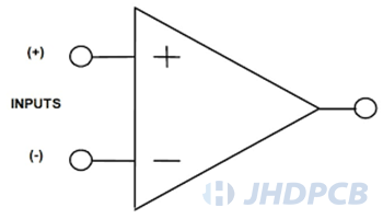
It is essential to create symbols from IEEE standards. Many designers lack understanding and experience with CAD schematic tools and often operate amplifiers for easy drawing. When creating a symbol, placing the input pin on the left and the output pin on the right is recommended. Similarly, the designer can put the power cord and ground pins at the top and bottom. Designers should be careful when flipping or changing the direction of the symbols, and the positive and negative terminals are likely to change their position. The common basic PCB design rules can be understood through our related blogs. Therefore, you should cross-check each sign with the manufacturer’s datasheet. - Heterogeneous schematic notation:
PGAF, memory, and microprocessors are called heterogeneous components. These components have many pins, such as data cables, input/output lines, address lines, control cables, and power cables. To preserve clarity and meaningfulness, designers ought to make different components of a single package. - Network connections:
At whatever point two wires frame an intersection and share an electrical connection, the crossing point must have an interface. Usually, the standard home is in each schematic plan.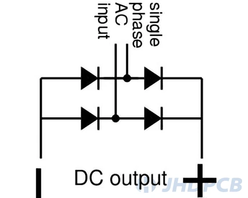
- Network label agreement:
The purpose of the schematic is to make it easier for designers to understand the circuit. Unnecessary network connections can be minimized when drawing the pcb design common symbols of an integrated circuit (IC) on a schematic. Rather than pulling handfuls of networks all over, the designer speaks to the organized title of a particular stick related to a snare on another gadget. These pins will have the same name. Assume that a pin with the same name is connected, improving the schematic diagram’s readability. Network naming is not required when the network is directly related to another IC on the same page. However, if you want to connect the network to an IC on another page, you need to name it. - Component placement:
Element placement in the schematic is one of the essential tasks. This will affect the subsequent creation of the bill of materials and IC package. - Design rules checking:
Design Rule Checking (DRC) is an intelligent feature of CAD that checks a design’s logical and physical integrity. The check is based on all empowered plan rules and can be done online at plan time. - Net table verification:
When the schematic design process is complete and the import into the layout begins, generate the netlist. Net table files can have two different extensions (.mnl & .txt). The .mnl files are machine-readable, .txt file displays all the electrical connections between components. It is recommended that the network be manually verified to avoid design errors. - Bill Of Material:
Currently, the CAD tool provides a critical feature called BOM creation. You can generate complete and sufficient BOM if the designer offers all input inputs in the tool when creating or importing parts from the library. The information on the bill of material can be MPN (manufacturing part number), package, supplier name, or supplier part number. It is recommended that all necessary information during symbol creation.
- Schematic list:
The logical schematic list, the most frequently overlooked point in creating a logical schematic diagram, is more relevant to the organizational process based on past design experience. Checklists reduce errors in diagrams and make plans more perfect. When designers draw circuits in CAD tools, you should note that the schematic design is the input of the layout designers. Layout designers expect to obtain an error-free schematic diagram so that the layout structure is reasonable and accurate.
A circuit board schematic is a diagram showing how all wires and components are connected in an electronic circuit. Like an outline for building a circuit or investigating a course, it offers almost all the information about how the circuit works. Reading electrical schematics is an instrumental skill. To better grasp how to read schematics, you should know the basics: symbol, reference indicators, network, and output.
The reference mark:
Reference designators are interested in recognizing names for each physical component. The proper utilization of REFDES tells the schematic per user, the sort of component, and the number of images per component. The industry standard arranges for the reference symbol comprises of a letter code demonstrating some kind of component, taken after by an interesting number.
Component symbol:
The symbols in the schematic represent the parts to be welded to the printed circuit board (PCB) during assembly. Now and then, they may moreover speak to PCB structures, such as through-holes or test focuses. Component symbols are usually industry-standard shapes or drawings that indicate what type of electrical component they are.
Network:
In schematic and printed circuit board parlance, a network is an electrical connection of PCB wiring. Networks are shown as lines that connect component symbol pins to other pins or networks.
Output:
Important outputs include netlists and bills of material (BOM). The network list is the main output of the PCB layout software and is used by the designer to guide the placement and Wiring of all circuits.
BOM is a spreadsheet or database that matches each REFDES in the schematic to a physical component and part number. The format of the BOM depends on the complexity of the schematic and part database and the type of output required.
- Select integrated circuits, transformers, transistors, and other significant electronic components, with many pins, which play an essential role in the course, and then extract from the selected reference hooks to reduce errors.
- If the element number is marked on the PCB because these sequence numbers have specific rules, the element with the same Arabic numerals is the same functional unit, so you should use the drawing. Rectifying recognizing components of the same accessible group is the premise for drawing the PCB layout.
- If the serial number is not available on the printing plate, it is necessary to number it yourself for easy inspection and editing. When designing printed circuit board package/component footprints, producers ordinarily orchestrate the components of the same functional unit relatively to play down copper thwart Wiring. Once you find a gadget with center usefulness, you’ll be able to discover other parts of the same accessible team.
- Correctly distinguish the printed board’s grounding, power, and signal wires. The contradicting conclusion of the rectifier is associated with the auxiliary of the control transformer, which is the positive anode of the control supply. The expansive capacity channel capacitor is primarily associated between the ground and the ground, and the capacitor shell incorporates an extremity check. You’ll be able to discover the control line and ground wires from the three-end controller stick. To avoid self-excitation and anti-interference, production line wiring printed circuit board by and large sets the establishing copper thwart within the most comprehensive (high-frequency circuit frequently expansive region establishing copper thwart), control copper thwart is two, and the flag copper thwarts the tightest. In addition, in electronic items where analog and advanced circuits coexist, printed sheets regularly isolated their establishing wires to make a free establishing network, which can too be utilized as a premise for distinguishing proof and judgment.
- To dodge over-the-top components, the circuit diagram wiring is interleaves, coming about in muddled pictures. You can widely use the power supply and grounding wires with terminal marks and grounding symbols. If there are many elements, you can draw the unit circuit individually and then combine them.
- When sketching, it is recommended to use transparent tracing paper and color pens to draw (e.g., ground wire, power cable, signal cable, component). When altered, continuously extend the color to create the drawing outwardly recognizably and analyze the circuit rapidly.
- Designers need to be proficient in the elements of some unit circuits and classical drawing methods (such as rectifier Bridges, voltage stabilized circuits, operational amplifiers, and digital integrated circuits). These unit circuits straightforwardly draw the system of the circuit graph, which can progress the drawing proficiency.
- When drawing the circuit diagram, find the circuit diagram of similar products for reference, and get twice the result with half the effort.
Znajdź legalne kasyna online w Polsce na pl.kasynopolska10.com/legalne-kasyna, partnerze naszej strony recenzującej kasyna online – kasynopolska10.
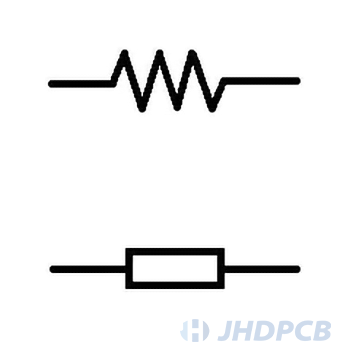
Resistors can be represented in two different ways, as follows. Designers should be careful to maintain the consistency of the symbols used. The resistance unit is the ohm, denoted by the symbol “Ω,” sometimes replaced by the letter “E .”The designer should ensure consistent unit representation throughout the overall design. Designers should enter all essential information about the component into the design instrument.
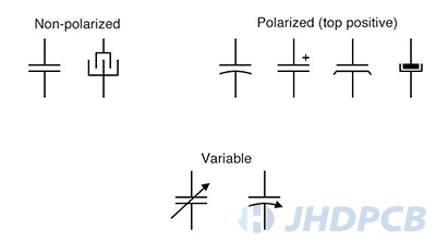
A capacitor has two terminals: positive and negative terminals. An incorrect polarity of a capacitor terminal may cause an explosion. The following figure shows the capacitance symbol in the IEEE standard. The designer should guarantee that the PIN code allotted to the image precisely coordinates the impression format.
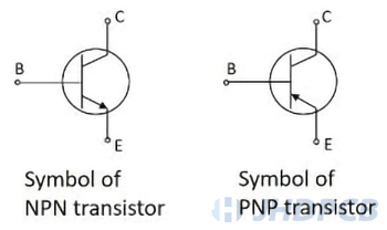
A transistor is a three-terminal semiconductor device consisting of a base, a collector, and an emitter. Designers should always refer to component data tables when mapping pin and footprint layouts to schematic symbols. When creating symbols, it is imperative to enter a depiction of the valuable component for future reference or when parts become obsolete and must be replaced.
It is essential to create op-amp symbols according to IEEE standards. Many designers lack understanding and experience with CAD schematic tools and often draw operational amplifiers based on convenience. It is suggested to put all input pins on the cleared out and all output pins on the correct. Similarly, power and ground pins can be placed at the top and bottom, respectively. Designers should be careful when flipping or changing the direction of symbols, as positive and negative poles will most likely swap their positions.
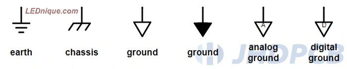
The symbols of the power supply and grounding pins are shown below. Because there may be a negative voltage on the board, use the “+” symbol to indicate the voltage. Designers ought to take after a standard and reliable tradition for speaking to voltage levels and their cross segments interior the silicon.
When we do Printed Circuit Board (PCB) design, we need to check all the items in the board schematic list in conjunction with DFM. We often need engineering judgment to select board size, cost, testability, and manufacturability. Here’s the list:
- Designer should verify the PIN and label of each element associated with the datasheet.
- Designer shall check all polarized components for polarity.
- Check whether the label and PIN overlap.
- Verify base, collector, and emitter pins for all transistors with datasheet.
- Verify the value, reference indicator, and position of the component.
- Ensure schematic notation is available (MPN, supplier name, supplier part number).
- Check the off-page connector.
- Find inter-table references.
- All integrated circuits are checked for decoupling capacitance, and ground pins are separated according to signal type (analog, digital, signal, ground).
- BOM check quantity and part number.
The PCB to schematic process is reverse engineering. It may be a multi-layered preparation focusing on PCB inquiry, reverse examination, and design innovation generation. This process is primarily used to identify and analyze the design principles behind the product. The most common method of reverse engineering a PCB involves disassembling a sample PCB and then analyzing it. Reverse engineering of a PCB consists in creating an initial drawing, scan, or photograph of the PCB and then uploading it to the appropriate reverse engineering software and programs. After uploading, build the layout of the PCB and use the layout to create the schematic.
- Step 1. Draw, filter or photo the PCB for picture preparation
The first step in reverse engineering a PCB is to draw, scan, or photograph the PCB. You need to take pictures with a dark background and photograph both sides of the PCB. - Step 2. Upload images
After taking the photo, you can upload it to the reverse engineering program. Before uploading the image, manually crop the image so that the picture shows only the PCB. - Step 3. Construct the layout
After uploading the image to the reverse-engineered PCB program, a 3D layout of the PCB needs to be built. The PCB layout shows how the system’s electromagnetic field distribution is arranged and how the circuit behaves. It also offers other parts that cannot show on the schematic, such as components, conduction elements, the arrangement of wires, and the plane of each layer. - Step 4. Creating a Schematic
The next step is to derive the schematic of the PCB. When you derive a circuit board schematic, you can see all the components of each circuit and board. The drawing is usually in the form of a two-dimensional CAD assembly drawing. When the schematic is created, you need to combine the sides of the PCB, arrange the tracks and symbolically label the elements.