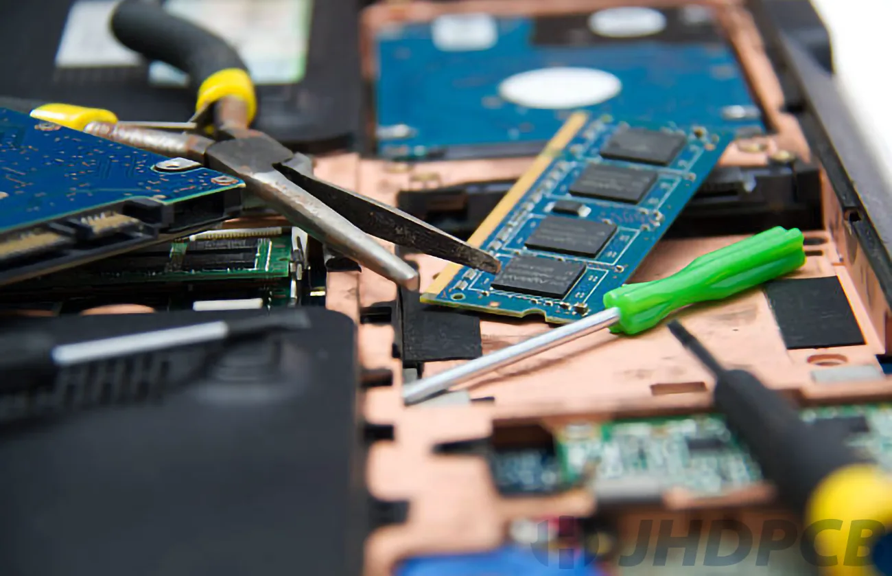
Fully understand PCB components: parts, codes and functions.

jhdpcb@gmail.com
What are circuit board components?
A printed circuit board component is an electrical part that goes into making the entire circuit board. PCBs consist of electrical elements such as diodes, capacitors, fuses, and resistors. For a PCB to function effectively, each component must play its role. If one part fails, then the PCB may fail to function as intended.
What are the common electronic components on PCB?
Each electrical component that makes up a PCB is essential to the operation of the device to which it will be attached. Various PCB board components, such as transistors, fuses, resistors, and capacitors, all contribute to the smooth operation of the device. If one of these components fails, the PCB as a whole will not function, which will have an impact on the product’s functionality.
PCBs can be single-sided (just having one copper layer) or multi-sided (having up to 20 or more layers). The PCB becomes increasingly complex as more layers are added, and the matching device it powers becomes more sophisticated. Moreover, more layers equate to more electronic parts.
Strong PCBs can undoubtedly support up to a dozen electronic components. But for newcomers, we advise starting with the 13 most typical parts.
Resistors
One of the most popular and likely easiest to comprehend components on PCBs are resistors. Their purpose is to block the flow of electricity by converting electrical energy into heat. They exist in a wide variety of designs and are built of a variety of materials, but the ‘axial’ form resistors with leads on both long ends and a body decorated with colored rings are the traditional resistors that hobbyists are most familiar with. These rings serve as a code to represent their resistance level.
Capacitors
Capacitors are the second-most prevalent electronic component after resistors on a PCB board. Capacitors momentarily store charge while resistors regulate it. See them as small batteries with limited storage. They have the ability to instantly lose and regain their full charge. In order to prevent data loss or reset, capacitors are frequently employed in the “filtering” process, which is the process by which backup power takes over when the primary power fails.
Capacitors in a PCB electrostatically store energy for subsequent release wherever power is required in the circuit. It functions by accumulating opposing charges (positive and negative) on two conducting plates, often made of metal, with an insulating substance sandwiched in between.
There are various kinds of capacitors, which are often grouped according to the conductive nature of the plates or the insulating substance between them. The majority of amateurs and beginners use radial, ceramic, or polyester capacitors. Click to learn more about PCB capacitor knowledge.
Transformers
A transformer’s job is to move electrical energy from one circuit to another while simultaneously raising or lowering voltage. The voltage is “converting,” if you will. The primary coil, for the initial or source circuit, and the secondary coil, for the circuit to which the energy is transferred, are twisted around a soft iron core similar to that of inductors. The overhead transmission lines’ voltage, which is frequently in the hundreds of thousands of volts, is stepped down by enormous industrial transformers on utility poles to the hundreds of volts generally needed for home usage.
Transistors
The essential building elements of contemporary electronics are thought to be transistors. A single IC chip may contain several billion. Nevertheless, transistors are merely electronic switches and amplifiers. They come in a variety of varieties, with the bipolar transistor being the most popular. They can also be divided into NPN and PNP variations. The base, Collector, and Emitter are the three pins on a bipolar transistor. As a current (often a tiny current) passes through an NPN-type device from the base to the emitter, another circuit is activated, causing a current (typically much bigger) to pass through from the collector to the emitter. The directions are switched in a PNP transistor. Field effect transistors, also known as FETs, are a different class of transistor that activates a different circuit using an electric field.
Diodes
A diode is a device that only permits current to travel in one direction, from the anode (+) to the cathode, much like a one-way street (-). In order to accomplish this, it has zero resistance in one direction and high resistance in the other. This feature can be used to prevent damaging current from flowing in the wrong direction. The light-emitting diode, or LED, is the most well-liked diode among enthusiasts. They are used to emit light, as their name suggests, but everyone who has tried to solder one knows that it is a diode, therefore it is crucial to get the orientation right in order for the LED to work.
Batterty
Without including the battery, the list of electronic parts that are mounted on or “passed through” a circuit board will not be comprehensive.
Searching for the letters “BT” on a battery’s body is the most popular method of identification. One of the passive electrical components, the battery serves as a power reserve and energy storage device for the printed circuit board (PCB).
The battery can be recognized in addition to having either “BT” or “B” imprinted on its body by either of the following:
- Verify whether the shrink-wrapping is blue or green.
- Any of the following shapes, including coin-shaped, rectangular, and cylindrical, can be used for the shape.
Integrated Circuits
Integrated circuits, or ICs, are exactly that—circuits and components that have been compressed into semiconductor wafers. The first calculators and the current generation of powerful computers, from smartphones to supercomputers, were made possible by the sheer amount of components that could be fitted onto a single chip. Often, they serve as a larger circuit’s brains. The circuit is often enclosed in a black plastic housing of various sizes and shapes, which may also contain visible contacts, such as leads protruding from the body or contact pads underneath, such as those found on BGA chips. If you want to know more about different PCB packaging technologies and chip classification, you can go to our corresponding page to view.
Crystal Oscillators
In clocking circuits, especially those that require reliable and accurate timing components, a crystal oscillator is essential. By creating the physical oscillation of a crystal material, it generates a periodic signal. Every crystal oscillator is required to vibrate at a particular frequency by design. It also shows to be a more stable, reasonably priced, and trustworthy alternative with a smaller form factor than other timing techniques. As a result, they are used as precise microcontroller timers or are assumed to be quartz wristwatches in various ways.
Features:
- A load capacitance of 18pF;
- a plus-minus 30ppm tolerance range for frequencies;
- Maximum resonant resistance of 40 ohms;
- A driving level of under 100 microwatts;
- An operating temperature range of -20 to 70 degrees Celsius.
Inductors
The letter “L” is a convenient way to identify inductors. They are also a two-terminal component that is mostly utilized to store electrical energy or magnetic field energy. When electric current flows through the inductors, energy is stored.
Although the inductors can be recognized by their initials, “L,” there may be additional technical issues that prevent the component from being recognized. You should focus more on the values or markings etched on it as a result of these.
Any of the aforementioned markers or values can be used to distinguish between inductors:
- H
- µH
- mH
SCR or Silicon-Controlled Rectifier
It is also known as a thyristor and is similar to diodes and transistors in appearance. In essence, it implies the cooperation of two transistors. The SCR has four silicon layers rather than three and has three leads (a cathode, an anode, and a gate). Instead of acting as an amplifier, it acts as a switch. The other difference is that current needs are applied consistently, especially for individual transistors, while just one pulse is required to activate the switch. Large levels of charge or power switching are another application where an SCR excels.
Features:
Forward Characteristics-
- When the voltage supply is raised, the CSR starts to conduct, creating a break-over voltage.
- The SCR may close at a lower voltage supply when the proper current flows through the gate.
Reverse Characteristics-
- Initially, a tiny leakage current is held by the anode current. The SCR starts to conduct heavily above a certain reverse voltage, which causes reverse breakdown voltage.
Potentiometers
Variable resistors come in the form of potentiometers. They are frequently seen in rotary and linear varieties. A rotary potentiometer’s knob is turned to change the resistance when the slider contact is moved over a semi-circular resistor. The volume control on radios, where the rotating potentiometer regulates the amount of current to the amplifier, is a famous example of a rotary potentiometer. The only difference between the linear potentiometer and a resistor slider contact slider is how resistance is changed. They are excellent when field fine-tuning is necessary.
Switches
Another well-known PCB component, second only to batteries, is a switch. Switches are frequently bought by many people—again, not only engineers and hobbyists—for informal, everyday uses. They are not only appropriate for printed circuit boards. These can be found in rooms, kitchens, remote controls, etc.
Consider switches and relays as on/off buttons. By opening and closing the circuit, they essentially regulate the current flow in a circuit. With just a flip of the switch, the circuit is activated, allowing current to flow to a room’s lightbulb. After one more flick, the circuit is shut off. The bulb loses power and is disconnected from the current.
At least a dozen different switch types exist, each with a unique physical design and appearance. Push-button switches, levers, and toggle switches are the more typical types. Box-type, rocker, micro, slide, and rotary switches are some further examples.
Sensors
We also have sensors, which are absolutely not the least of these. These are rather simple electronic components in that they react appropriately when they “detect” physical input or environmental changes. The kind of input might be anything from variations in pressure, noise, motion, and more to changes in heat, light, and moisture.
The sensor’s reaction takes the shape of an electrical signal that corresponds to the kind of change it has identified. Other circuit or PCB components then receive this signal.
These sensors then produce an output, if designed to, in the form of extra signals conveyed electronically for further reading or processing, or human-readable displays.
Electrical energy is often converted from physical energy using printed circuit board sensors. This qualifies them as converters in a way. Being highly adaptable, sensors can take many different shapes. These may even be diodes, similar to the red LED light on a remote control for a television that indicates whether the gadget is on or off. Sensors are frequently used in practical applications such as humidity monitoring, air quality detection, motion sensors, and automatic lighting.
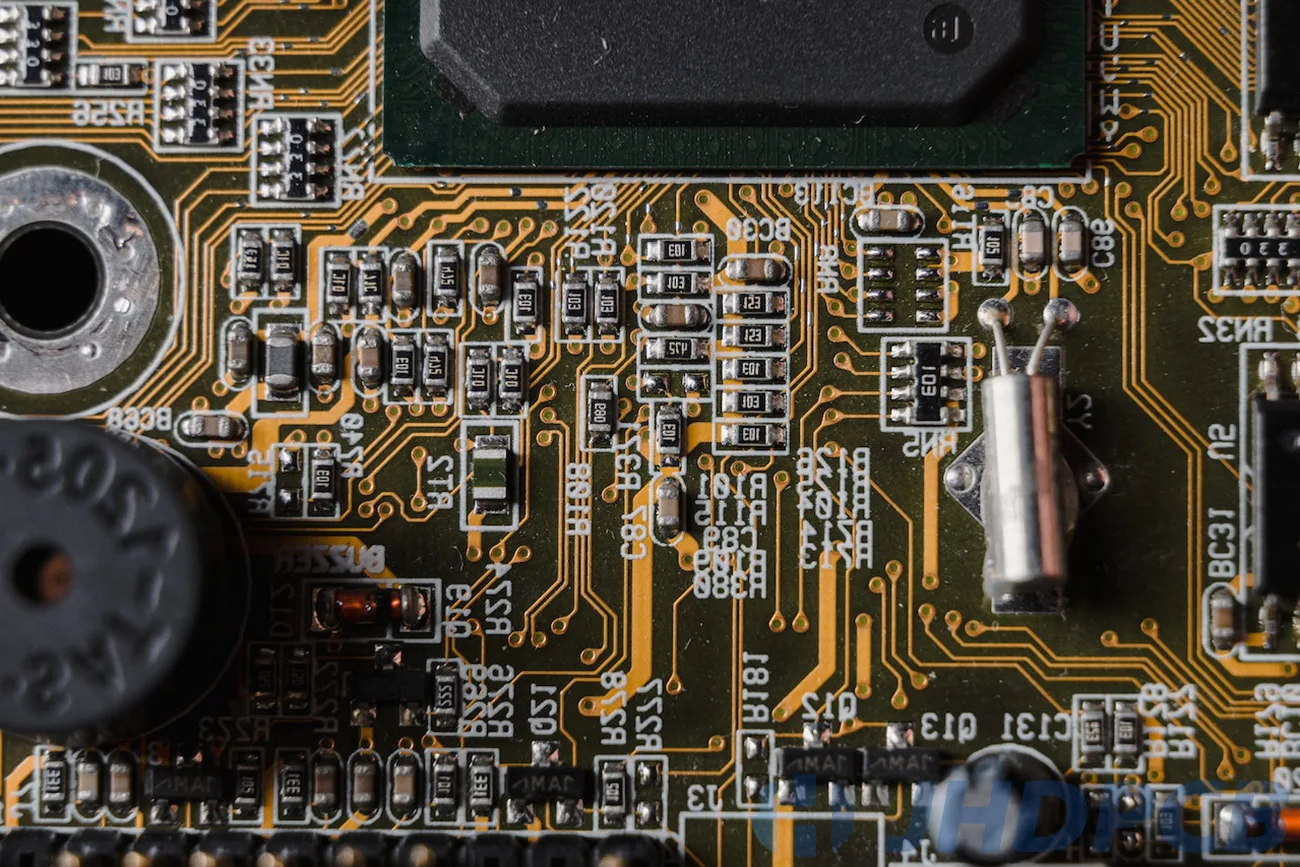
Common PCB components codes.
The table below lists pcb component designators commonly used:
| Designator | Component type | Designator | Component type |
|---|---|---|---|
| A | Separable assembly or sub-assembly (e.g. printed circuit assembly) | LS | Loudspeaker or buzzer |
| AT | Attenuator or isolator | M | Motor |
| ATT | Attentunator | MOV | Metal Oxide Varistor |
| BR | Bridge rectifier | MK | Microphone |
| BT | Battery | MP | Mechanical part (including screws and fasteners) |
| C | Capacitor | OP | Opto-isolator |
| CB | Circuit Breaker | P | Plug (most-movable connector of a connector pair), Plug connector (connector may have “male” pin contacts and/or “female” socket contacts) |
| CN | Capacitor network | PS | Power supply |
| D,CR | Diode (all types, including LED), thyristor | Q | Transistor (all types) |
| DL | Delay line | R | Resistor |
| DS | Display, general light source, lamp, signal light | RN | Resistor network |
| G | Oscillator | RT | Thermistor |
| J | Jumper or Jack | RV | Varistor, Variable resistor |
| L | Inductor | S | Switch (all types, including buttons) |
| F | Fuse | T | Transformer |
| FB | Ferrite bead | T | Thermocouple |
| FD | Fiducial | TP | Test point |
| FL | Filter | TUN | Tuner |
| G | Generator or oscillator | U | Integrated circuit (IC) |
| GN | General network | V | Vacuum tube |
| H | Hardware, e.g., screws, nuts, washers | VR | Voltage regulator (voltage reference), Variable resistor (potentiometer or rheostat) |
| HY | Circulator or directional coupler | X | Socket connector for another item not P or J, paired with the letter symbol for that item (XV for vacuum tube socket, XF for fuse holder, XA for printed circuit assembly connector, XU for integrated circuit connector, XDS for light socket, etc.) |
| IR | Infrared Diode | XTAL | Crystal |
| J | Jack (least-movable connector of a connector pair), Jack connector (connector may have “male” pin contacts and/or “female” socket contacts) | Y | Crystal or oscillator |
| JP | Jumper (Link) | ZD | Zener Diode |
| K | Relay or contactor | L | Inductor or coil or ferrite bead |
Click here to view more detailed knowledge of PCB component symbols.
How to place PCB components?
Here are some suggestions for component placement:
- Understand Mechanical Constraints.
It’s crucial to take the enclosure that the PCB must fit inside into account while designing the PCB. Regarding the size and design of the board, it is essential to know exactly where mounting holes and edge connectors should be placed. - Consider Assembly Constraints.
Consult the manufacturer before creating a board to learn how the board and components will be put together and tested. The manufacturer needs to outline the assembling procedure and specify how much room is available on the board. - Don’t Place Integrated Circuits Too Close Together.
The recommended distance between each IC on the board is between 0.3500″ and 0.5000″, with even more room for bigger ICs. When ICs are placed too closely together, there may not be enough room for connection pin routing, which requires time-consuming design reorganization. - Use a standard orientation for the components.
For the manufacturer, this makes the process of installation, inspection, and testing simple. Similar components should be oriented in the same direction to avoid disrupting the soldering process and causing certain parts to not be soldered at all, resulting in shorts and open circuits on the board. Integrated circuits always feature a reference pin, regardless of their footprint or quantity of terminals. Designers must ensure that the ICs are all oriented in the same direction in order to streamline the PCB layout and make the assembly process simpler. As a result, positioning mistakes are decreased and assembly efficiency is improved. More generally, the rule is to solder components that are comparable (including passives) in the same direction to maximize efficiency and reduce error. - Reduce Connectivity Routes to a Minimum.
It is advised to bundle parts to reduce crossings and crisscrossed connecting parts for a simpler and more uncomplicated routing method. - Group components by function.
Similar-functioning components ought to be grouped together. For instance, converters, LDOs, and other similar devices that produce a lot of heat and high currents should all be put together in the same power management area. When using signals with high switching frequencies, the analog and digital components, as well as the power supply portion, should be kept apart. Moreover, components that produce electromagnetic noise or radiation need to be kept away from signals that are more sensitive. It also enables better control of the return path by classifying components in accordance with their functional groups. - Separate the different areas from each other.
Digital, analog, radio frequency (RF), and power component-containing PCB areas should be maintained apart from one another.
By keeping the various functional domains apart, crosstalk phenomena that threaten the signal’s integrity are prevented from developing between the combined analog and digital signals. The simplest method for preventing the overlap of analog and digital traces is to maintain non-homogeneous components in different locations. The analog and digital masses must adhere to the same guideline in order to prevent confusion. - Keep the components away from heat sources.
MOSFETs, IGBTs, PMICs, and voltage regulators generate a substantial amount of heat when used in high power applications. It is usually best to keep other components away from the power components, even if you add additional vias to help with heat dissipation. The same is true for heat-emitting equipment like operational power amplifiers. - Create solid ground planes.
Because interruptions would encourage the start of signal and power integrity problems, ground planes should always remain uninterrupted. Extreme care must be given while positioning components across the interruption if it was unable to keep the ground plane uniform. For instance, high-speed signal transmission lines shouldn’t cross ground plane discontinuities because doing so would cut off the signals’ return path.
Avoiding an excessive number of routes that could potentially block the signal return paths, in addition to the usage of solid ground planes, is another criterion that aids in the creation of safe and clearly defined return paths. To adequately secure the control signals and lower the chance of interference, it is recommended to also insert a low impedance link if the ground plane has been positioned on an intermediary layer. - What to place near the edges of the PCB.
The connectors, especially if they need to be fixed with screws, must be placed close to the edges of the PCB. This makes board construction and installation simpler and prevents cables from coming into contact with other PCB components unintentionally. - Leave enough space for the traces.
Increasingly smaller PCBs are needed in electronics due to the present trend, which is most noticeable in the wearables and portable devices industry. Circuits can only be reduced to a certain degree in size, and this optimal size must always be observed. Otherwise, routing all traces becomes all but impossible. So, when putting the components, care must be taken to leave enough room on the PCB for the passage of copper traces, especially in close proximity to components with a lot of pins. - High-speed signals.
To make the routing of the traces easier, components that handle high-speed signals must be grouped together in one section of the PCB and positioned next to one another. Short and straight traces need to be used to connect these signals.
Decoupling capacitors must also be linked to the power ports of high-speed devices that consume a lot of current, such as CPU, FPGA, and GPU. The positioning of these capacitors can be more challenging on digital circuit boards or when there are components with BGA packages present.To prevent oscillations on the power and ground signals and to address any power supply integrity issues at the source, bypass capacitors must be positioned as close as feasible to the VCC pins of the active components. - Thermal management.
The quantity of heat produced by components during operation must be taken into account when situating them. The core of the PCB should be used for heat-generating components like CPUs so that the heat is distributed uniformly around the board. In order to prevent the cooling of the hottest components from being impeded by the presence of larger components, it is also important to pay attention to the path taken by the air flow. Also, it is a good idea to set aside enough room right away for the installation of any heat sinks or other equipment intended to enhance thermal dissipation.
Basic knowledge of electronic components affecting PCB layout.
In its simplest form, a PCB layout refers to the transfer of a course from a breadboard to a permanent and stable physical condition. Electronic circuits can be divided into a number of groups, components, and types, as noted below.
- Categories of electronic circuits.
Active parts – Active parts do rely on the system’s energy sources. Active sources are capable of supplying the circuit with electricity.
Components that are passive cannot supply energy to an electrical circuit. They cannot magnify signals because they do not rely on DC sources of power like the active components do. - Electronic circuit elements.
The following are important components of electronic circuits. The following are some of the fundamental electronic circuit components you should be familiar with while working with a PCB:
The flow of electrons is known as electron current. Electrons do move from negative terminals to positive terminals on a circuit board. Traditional wind acts like a positive current to move current.
Power source: Choosing the type of power source that is best for your device is crucial when it comes to a power supply. You can select between an AC input and a DC input depending on where you plan to use your gadget.
Electric loads are more like electrical components that use electricity. It’s distinct from an energy-producing power source like a battery or generator. Loads on a PCB include things like lights and appliances. - Types of electronic circuits.
Many kinds of electronic circuits exist. Among the most significant ones are the following:
Electricity only travels in one way in a direct current electronic Board. Direct current is usually used in smaller PCBs.
Alternate current: Electricity flows in both directions while switching frequently in an alternating current printed circuit board (PCB). Besides from the fact that it can travel great distances without losing energy, AC is also simple to create.
Series circuits are created by connecting components in a loop one after the other. Only one terminal serves as the means of connecting the pieces. The breakdown of the entire circuit is eventually caused by a break in the link.
Contrary to series circuits, parallel circuit PCBs require the positioning of parts in distinct branches. The connection between pieces in parallel circuits is made through both ends, although in various chapters. Just the damaged branch is impacted when a relationship in a parallel circuit breaks.
Common PCB components codes.
How to choose PCB components?
How To Identify Components Step-by-Step?
Like to most things in life, breaking a task down into smaller components makes it easier to identify the components.
- Determine board usage.
Try to recognize the board as a whole first. What does it serve? Is it a daughterboard, a motherboard, or does it serve some other purpose? Codes that facilitate this operation are marked on some boards. For instance, the DMCB board shown below is a GE Mark V system’s DOS Main Control Board. This is a common acronym found on GE boards. They could aid you in understanding the board application.
Find passive parts next, such as capacitors and inductors. Next, look for potentiometers and resistors. They will typically be marked with an ohm measurement. - Identify the Parts.
Find passive parts next, such as capacitors and inductors. Don’t worry; images will be included in this post later. Next, look for potentiometers and resistors. They will typically be marked with an ohm measurement.
Oscillators (cylinders or boxes commonly designated with X or Y), transformers (T), diodes (D), and relays are further distinguishable parts (marked as K).
Check the board now to see whether there is a fuse. Fuses are frequently opaque or clear tubes. Next, make an effort to spot any batteries or transistors. - Circuit board connector.
Any board connectors should be noted. The board can be connected to other circuit boards, larger systems, or external components using connectors.
The most popular connectors are backplanes, terminal blocks, pin headers and the sockets that take them, and jacks or plugs. There are so many different types of connectors that you could spend months learning about them all.
Lastly, identify the board’s processor and additional integrated circuits. Many ICs will include a label or ID with the manufacturer and part number.
JHDPCB offers 14 crucial suggestions for choosing PCB components.
- Bill of Materials — Helpful for Virtual Parts.
When you need it, the primary function of the BOM will assist you in creating a virtual pcb parts list. It is also useful to permit the designing division to review virtual parts. Power and ground signals may be present as virtual components. These components won’t be moved to the layout section; they will unquestionably be included in the schematic environment. If only being used for simulation, the parts are displayed in the virtual section; if not, replace with the ones that have footprints. - Reference Designators — Check BOM Data Report.
The primary function of reference designators is to assist in the organization and review of the BOM by ensuring that all items are quickly numbered. Make sure your BOM data is accurate and evaluate it. Verify that all parts are there and that nothing is missing before moving on to the design phase. - Basic Design Outline.
Before making expensive prototype designs public, design outlines serve to provide a general understanding of where components are positioned. Also, this will provide a fundamental grasp of the part placement, the necessary heights, and whether the whole plan will function both completely and electrically. - Requires a suitable ground plane.
Make sure your design includes appropriate ground planes and bypass capacitors first. You will require the proper capacitor, including the right size and frequency, depending on the PCB’s intended use. Also, avoid using capacitors in your design and demand solid, good ground planes. - Basic schematic diagram.
Before making expensive prototype designs public, design outlines serve to provide a general understanding of where components are positioned. Also, this will provide a fundamental grasp of the part placement, the necessary heights, and whether the whole plan will function both completely and electrically.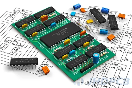
- Requires a suitable ground plane.
Make sure your design includes appropriate ground planes and bypass capacitors first. You will require the proper capacitor, including the right size and frequency, depending on the PCB’s intended use. Also, avoid using capacitors in your design and demand solid, good ground planes. - Consider the footprint.
The use of schematics is crucial while constructing a PCB. You can go about more easily if you use the schematic. Discover how to maintain and repair a PCB if it is damaged, as well as where each PCB is installed. - Follow acceptable grounding practices.
When designing a PCB, you need to follow some grounding rules. Grounding is essential in your design process. Without a solid ground, you may not be able to ensure a clean signal passing from one component to another. Some basic grounding practices include leaving nothing floating, grounding before routing, and minimizing series vias. - PCB welding – choose the right components.
PCB soldering may appear to be a simple process, but if done incorrectly, you risk producing low-quality boards. In mass production, there are two commonly used welding methods: wave soldering and reflow soldering. If you want an excellent board, be sure to choose the appropriate gear. Ensure that both the soldering iron and the solder are of the finest caliber. Your PCB could not work if you choose the incorrect components. - Separate lead from lead-free components.
Leaded solder has long been a preferred material in electronics manufacture and rework. But over the last few decades, there has been a rise in environmental worries and issues related to lead-based products. The scale of the project determines whether to use lead-containing or lead-free components.
You might have to choose lead-free components, though, in light of recent government regulations. It is well recognized that lead-free components are safe for people and the environment. In-depth exploration of the importance of solder to PCB. - Is padding required?
The exposed portion of a printed circuit board, or PCB pad, is where components are mounted and soldered. Depending on the component being soldered to that place, pads come in a variety of forms and shapes. Filling prevents potential flashovers and electrical conductor tracking. - Pad design matches the lead setup on the component.
It’s really that simple. The part’s leads and the pad design must be compatible. To prevent imbalanced solder junctions, make sure the pads closely match the lead configuration. - Consider component package options.
Choose Surface Mount Technology or Plated Through Hole assembly? Component selections can be altered while the design is being made. The organization of the PCB as a whole can benefit from choosing which components will use Surface Mount Technology and Plated Through Hole during the design phase. There will be problems with component pricing, accessibility, component area density, and power dissipation, among other things, that will effect your design when you consider component choices.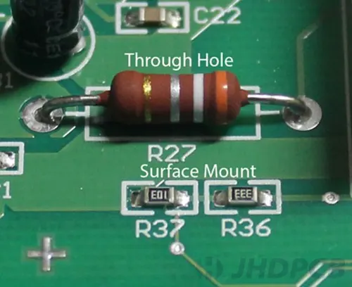
- Review Spare gates.
In order to prevent inputs from floating, the majority of spare gates should typically have their inputs coupled to a signal. Make sure to check any spare gates to make sure that, if necessary, unwired input sources can be attached. The entire system might occasionally not function properly if the input sources are left to float.
How to find shorted components on PCB?
During the PCB prototype testing phase, developers need to comprehensively identify short circuits in hundreds of traces and components in the PCB design. It’s not an easy job, but JHD knows where to look.
- Signs of a Short Circuit.
How can short circuits on a PCB be detected? Depending on where it might be shorted, you could have a range of symptoms. For instance, when you switch on the PCB, you might hear a loud “pop,” then there might be arcing and a broken trace. These concerning signals typically allude to power line short circuits.
Sometimes the red flags are less obvious, and you won’t see them until you’re inspecting the functionality of a particular circuit. Two input pins that are shorted to one another won’t provide any indicators during a test power-up. You will simply observe that the circuit is malfunctioning if the inputs don’t produce the desired outcomes. - Visually Scan the PCB.
You may occasionally detect glaring shorts, such as a solder junction between pins or copper portions that have not been completely etched out. Some of the shorts are as thin as a hair, so you might want to use a magnifying lens. - Look for Signs of Burnt Components.
Certain components may burn as a result of a short circuit. Telltale indications that a short circuit is present include a broken integrated circuit (IC), blown capacitor, or the well-known noxious smell of burnt components. Find the faulty component, remove it, and look at any traces that are connected to it. Either the damaged component itself or the traces that connect it will have the issue. - Probe with a Multimeter.
Your best ally in finding a short circuit will be the multimeter. Verify the consistency of each of the traces you suspect are shorted. Even while it doesn’t provide the precise location of the brief, it gives you a general sense of where to go first. - Use a Thermal Camera.
The precise locations of the shorts can be located with the aid of a thermal camera, which employs infrared technology. If the board has been powered on, the short circuit could conduct an excessive amount of electricity and get hot.
You can detect the hotspots with a thermal camera and then confirm them visually. However, manual inspection will not be possible if the short develops in the inner layers.
What Causes Short Circuits on a PCB?
Short circuits on your PCB should be avoided at all costs, which calls for identifying the underlying reasons. During manufacture or assembly, some short circuits can occur. A hairline short develops during manufacture when a thin copper line is left behind.
Reflow soldering might also result in short circuits. Two pins that are relatively near to one another could unintentionally connect due to solder paste. Occasionally, PCB design errors occur where traces between various nets are unintentionally joined.
In other cases, the short is caused by malfunctioning components rather than the PCB. The problem can be fixed by removing the problematic component.
Using the appropriate PCB design and analysis software will help you reduce short circuits brought on by design errors, even while manufacturing and assembly are partially out of your control. Before completing the design, check your nets for short circuits using OrCAD PCB Designer’s DRC function.
PCB parts aging problem.
Reasons and solutions for the aging of parts of PCB.
Another significant contributing reason to PCB failures is the circuit board’s age. Several of its parts will start to break down as it gets older. For instance, a failing capacitor may begin to cause issues with the power supply that are sporadic. While PCB failures brought on by aged boards are unavoidable, costs can be kept under control by switching out old components for fresh ones. Thankfully, many of the issues brought on by aging may be fixed for a small portion of the cost of a brand-new PCB. Instead of creating and putting together brand-new PCBs, it might be more cost-effective to swap out outdated components with more recent ones. Also, using proper soldering procedures might increase a PCBA’s lifespan.
Purpose of PCB Aging Tests.
To collect information for evaluating the long-term dependability of a PCBA that may be used in continuous operation for more than 100,000 hours, PCB aging tests are performed (at least 20 years). These tests assess a PCBA as a whole, revealing the general dependability of the bare circuit board, its parts, the solder and mechanical components, as well as any other materials used in the PCBA’s creation. A PCBA obviously cannot undergo constant testing for 20 years, so test engineers will conduct simulations of real-world conditions or other tests to assess long-term stability.
The documentation process used by PCB manufacturers and design teams has grown more complicated over time as performance requirements and fabrication requirements have done as well. A design team can quickly generate their test and fabrication data from their PCB component layout with the appropriate design software. Project documents can be used to specify and readily communicate with manufacturers important criteria like the dependability of solder joints, necessary PCB materials, use of conformal coatings, and a variety of test methods.
PCB Aging Testing Technology and Methodology.
There are four standard PCB aging assays that are all thermally based. These exams consist of:
- Burn-in testing: a strategy for predicting which assemblies and/or parts will fail first using statistical methods.
- Highly accelerated life testing (HALT): Here, the objective is to severely overwork a gadget until it fails. In the real environmental conditions where the device will be deployed, this simulates overoperation.
- Highly accelerated stress testing (HAST): The design is stressed until it completely fails, similar to HALT.
- Highly accelerated stress testing (HASS):Employs the same environmental pressures as in HASS, but at lower levels, and ordinarily follows the conclusion of a full HALT test.
There is a standard process that all PCB aging test procedures follow:
- Maintain a batch of discrete components or PCBAs at an elevated temperature for a predetermined period of time (typically multiple hours or days)
- Check the batch for flaws or failed components.
- Discard the defective parts and inspect the remaining PCBAs and components.
- Continue doing this until the premature failure group has been found.
- Statistically analyze the data to determine the premature failure rate.
- Examine the damaged components to identify the underlying issue.
How to purchase PCB components?
You must decide what you’re going to purchase. While purchasing electronic components, you must be aware of the components’ look, model, performance, and other key factors.
- Find an open, transparent, and honest website.
You can locate some websites that focus on samples by first using the search feature to look for “component sample retail” websites (or small batches). Some websites will prominently display the price, while others won’t. The most practical option is if the price is already listed on the website. Often, there is no cost attached. To contact the pricing, you must email or call each person individually. For future use, all details, including the URL of the website, must be recorded in writing, ideally in a larger notebook. - Multiple price comparisons.
Go to another website if some components can’t be searched on one. Consider using a different model in its place if you can’t find a specific one. Typically, all you need to do to determine the market pricing for any given component is to contact three or four dealers (outside of your immediate area). This type of quotation is typically the lowest price the manufacturer will take, and it is very rarely negotiable: the quotations within the same region differ little, those within different provinces differ little, and the quotations for various models within the same region differ significantly. Big: Based on the entire quotation analysis, you can choose which component or components to purchase. In order to reduce the number of buyers, the price should be reduced accordingly, and the delivery charge should be the lowest, you must first filter your shopping list by category. - Payment and delivery.
You have determined the type and model of the component. And after completing the supplier assessment, you can directly purchase. The order will be shipped once the supplier confirms the order. - Inspection.
As soon as the items arrive, they should be inspected; the model should be checked first, followed by the quantity. There is typically nothing improper as long as there are few options available for purchase. Spot checks are then conducted to test critical parameters. If there is an error, please contact the supplier immediately for repair or replacement.
If you are not very professional and don’t want to trouble, you can contact JHD’s customer service staff. We are willing to source components in China for our customers after the PCB manufacturing is completed. We will use our own experience to review the quality of components, and use our own brand advantages to help you reduce component procurement costs.
How to solder PCB parts?
Step 1: Prepare the equipment and materials needed.
- A soldering station or a stand with a 20–40 W soldering iron
- Solder lead 60/40 (22 gauge preferably)
- Soldering flux
- Pitch bending tool
- Damp sponge
- Fine sandpaper or steel wool (to clean connections before soldering)
- Nippers (or cutter)
You’ll also need a solder braid/wick or desoldering pump to remove melted solder if you’re disassembling soldered components on PCB board.
Step 2: Turn on the soldering iron and let it warm up.
Step 3: Wipe the hot bit on the wet sponge to clean the solder tip.
Step 4: Melt some solder onto the solder bit to give it some color. Tinning aids in the flow of heat from the solder tip to the joint.
Step 5: To ensure that solder will attach to the copper pad on the PCB, make sure it is clean. If it is not, clean it with steel wool.
Step 6: An element for a PCB is soldered on.
Put the hot soldering tip on the PCB copper pad and component lead to heat them up before soldering an electronic component to it. Any solder that touches them will melt, run into the center of the pad, and fill the space left surrounding the lead. After finished, take out the tip first, then the solder material. A connection can be soldered in a matter of seconds.
Step 7: After soldering the components, snip off excess component leads with a pair of nippers because leads coming into contact with one another can cause short circuits.
Step 8: Use a cleaning substance, such as isopropanol, to remove any extra flux that has been applied to the PCB.
Our business offers effective and dependable automated wave and reflow soldering in this area in addition to assembly line equipment. Also, there is workforce training in place to strictly regulate welding standards and prevent welding errors. to guarantee PCBA quality.
How to Remove PCB parts?
- Step 1: Use a solder extractor, often referred to as a solder sucker, to remove solder from a junction, such as if the incorrect component was inserted into the PCB.
- Step 2: By pressing the plunger down against the spring, prime the solder sucker. Take up the solder sucker and soldering iron with one hand each.
- Step 3: Using the soldering iron, warm the junction that needs to be desoldered. Keep the solder sucker’s tip close to the joint so it is ready to use.
- Step 4: Press the button on the solder sucker when the solder melts to suck up the molten solder. To give the solder sucker easier access to the joint, it can occasionally be helpful to remove the soldering iron.
- Step 5:The heating and sucking procedure should be repeated if all of the solder is not removed. Remove the desoldered component after letting the board cool for a little while.