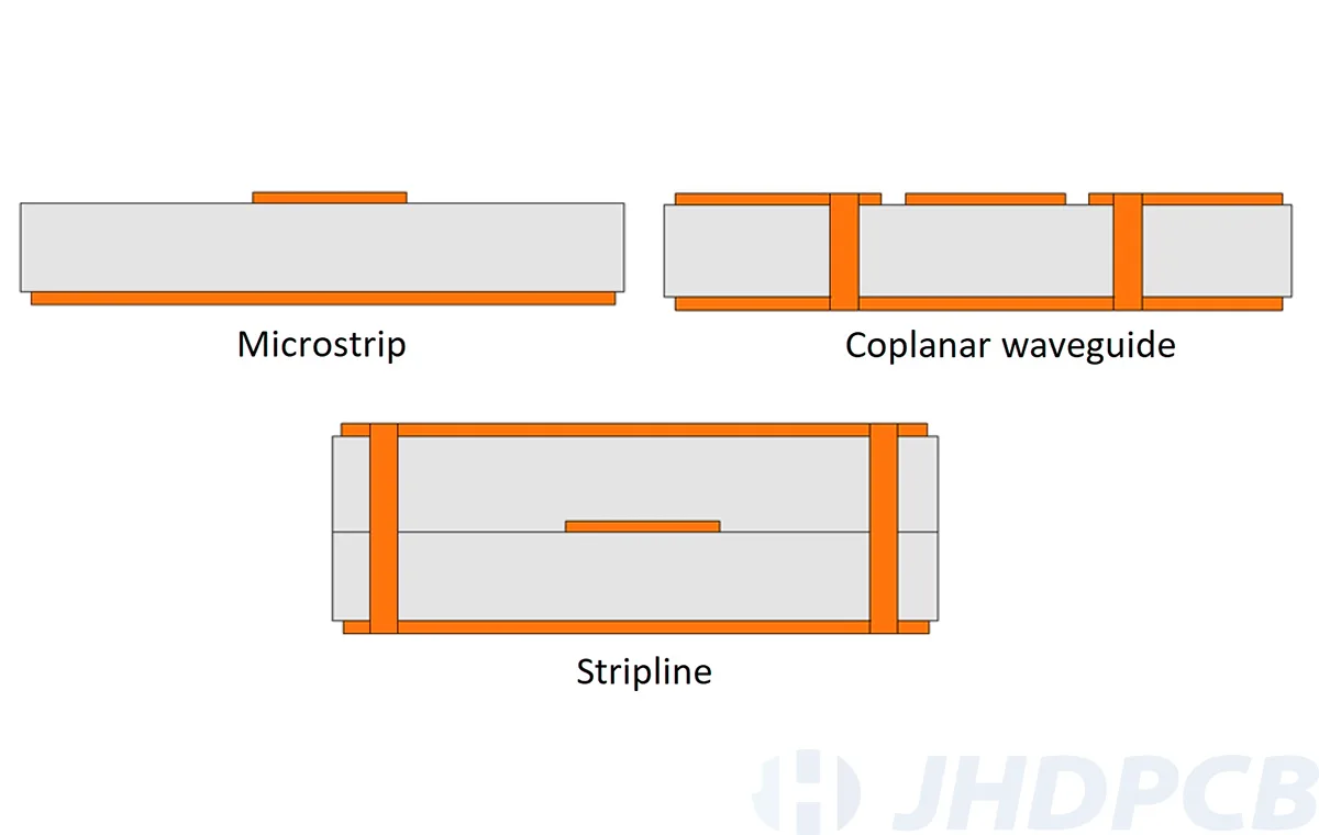

PCB Microstrip is a commonly used type of electrical transmission line for conveying microwave-frequency signals. It consists of a conductor separated from a ground plane by a dielectric layer like FR4, polyimide, PP, or Coverlay. Microstrip lines can be fabricated using various technologies and can be easily integrated with microwave devices, making them a popular choice for transmission lines. In addition, microstrip lines can be used to create a range of microwave components such as microstrip antennas, microstrip couplers, microstrip filters, and power dividers, with the entire device existing as a pattern of metallization on the substrate. They are known for their ease of manufacturing, ability to maintain signal integrity, and compatibility with other components on the PCB.
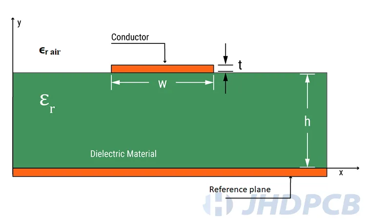
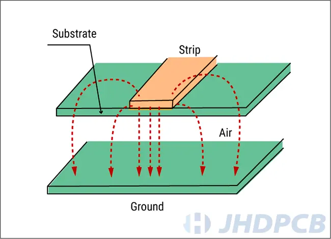
The microstrip structure comprises of a conductor with a specific width (w) and thickness (t), along with a dielectric substrate that has a certain thickness (h) and permittivity (εr).
The mode of propagation of microstrip:
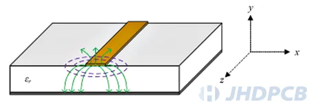
Microstrips propagate in a Quasi-TEM (Transverse Electromagnetic) mode, which means that the phase velocity, characteristic impedance, and field distribution in the cross-section vary with frequency. The field lines are concentrated in the region between the conductor and the ground plane due to the dielectric substrate (commonly thickness d < λ). There are field lines present in the air region above the conductor. This leads to quasi-TEM modes of propagation, where dispersion occurs as a function of wavelength. The following image shows the dispersion of microstrip modes due to the quasi-TEM propagation.
Microstrip transmission lines do not have exact analytical solutions and must be analyzed numerically. However, numerical analysis results can be used to create an analytical approximation of microstrip transmission line behavior. Here are some commonly used microstrip equations in line design:
Microstrip Transmission Models – Approximation models have been developed to estimate the characteristics of microstrip transmission lines.
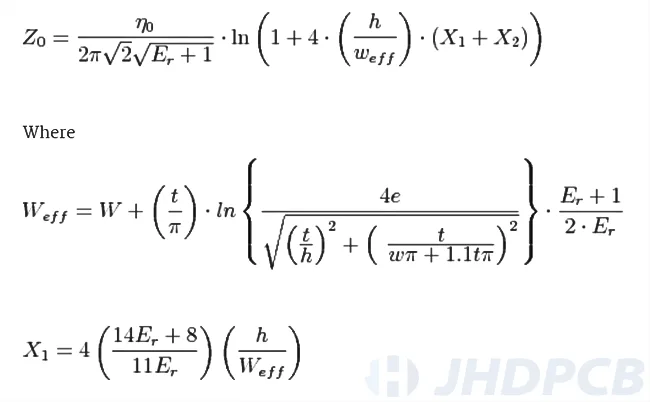
Frequency-dependent effect of the microstrip effective dielectric constant – Because of the quasi-TEM nature of microstrip lines, the propagation constant is not a linear function of frequency. The frequency variation of the effective dielectric constant is a significant factor to be considered, especially with the introduction of higher order modes at high frequencies. A popular model for describing the frequency-dependent effect of the effective dielectric constant is given by the formula:
Microstrip impedance formula (Z0) – For a given PCB laminated and copper weight for the width of the signal trace (w), the equitation given below can be used to deign a PCB trace to match the impedance required by the circuit. The characteristic impedance (Z0) for a signal trace with width w and thickness t, separated by distance of h from a ground plane by a PCB dielectric with a dielectric constant (εr), can be calculated using the following formula:
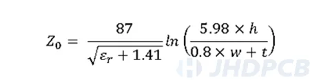
Where:
- w is Width of the copper trace (flat copper conductor)
- h is Distance between signal trace and ground plane/Dielectric substrate height.
- εr is Relative permittivity/dielectric constant of the dielectric material.
- εe is microstrip Effective dielectric constant.
- Z0 is Characteristic impedance of the microstrip in ohms (Ω).
Note:
All dimensions are in mils.
The characteristic impedance of the changes with an increase in frequency.
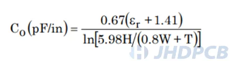
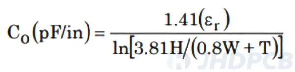
Characteristic capacitance of a microstrip line:
Dielectric constant of substrate material (εr):
The dielectric constant is defined as the ratio of the capacitance of a capacitor that is dielectric to the test material to the capacitance of a capacitor that is dielectric to vacuum (or air). The dielectric constant of a PCB affects its impedance. Low and stable permittivity is suitable for high frequencies and control impedance, while a varying or higher dielectric constant can affect impedance in unpredictable ways.
Effective dielectric constant (εeff ):
The effective dielectric constant, also called Keff, of a microstrip transmission line is influenced by the fact that some of the electric fields from the microstrip conductor exist in air. As a result, the Keff is typically lower than the substrate’s permittivity constant, and falls somewhere between that of the air and dielectric. The electric energy stored in the microstrip arrangement is split between the air and dielectric, contributing to the effective permittivity. The microstrip line is dispersive, meaning that as frequency increases, the effective dielectric constant also increases towards the substrate, causing the phase velocity to decrease. Most of the electric fields remain within the substrate, but a certain amount of energy is also present in the air above the board. The Keff of a microstrip can be calculated using the following formula:
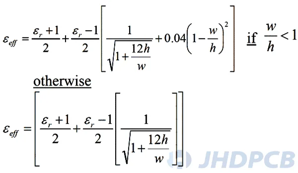
Where:
- εr is the dielectric constant of the dielectric material.
- h is the substrate thickness.
- w is the width of the microstrip.
Note: that εe ≠ εr; in fact, 1 <εe <εr
Capacitance:
The characteristic impedance of the microstrip line is significantly influenced by the capacitance between the signal trace and the ground plane. An increase in capacitance causes a reduction in the line’s impedance due to the capacitance acting as a shunt impedance that lowers the overall impedance of the line.
Thickness of dielectric substrate (h):
The thickness of the substrate has a significant impact on the impedance of the microstrip line since it affects its capacitance. An increase in substrate thickness causes the capacitance to increase, resulting in a decrease in impedance. In fact, even a small increase of 0.025mm in laminate thickness can cause impedance to vary by 5 to 8 Ω.
Width of traces (W):
When designing a PCB, the trace width, which includes the width of the copper foil and its coating, directly impacting the trace’s impedance. Increasing the trace width leads to a decrease in impedance. PCB designers consider several factors, such as capacity and temperature rise, when determining the appropriate trace width. If they have a specific impedance value in mind, they can design for that too.
Thickness of traces (t):
The thickness of the trace has an impact on the impedance of the microstrip line due to its effect on resistance. When the trace thickness increases, resistance also increases, resulting in a decrease in impedance.
Suspend the substrate in air:
Suspending the substrate over the air shows that the substrate is separated from the ground plane, which increases the separation between the signal and ground paths. This technique enhances the tendency of the microstrip line to radiate, especially at discontinuities. In the gap between the substrate and the ground plane, the electromagnetic field exists. The insertion loss of the microstrip is reduced due to the absence of dielectric loss in the air compared to typical circuit board substrates. The effective dielectric constant is also reduced, resulting in wider microstrip lines with lower current density and lower ohmic loss. However, it’s important to note that this technique is only effective up to a few GHz, and reducing the width of the microstrip line will increase losses.
Apply multi-layer microstrip line:
The microstrip geometry is effective for conducting EM waves at low frequencies, but its application is limited due to losses at higher frequencies, making it unsuitable for use at THz frequency. However, a multi-layer microstrip line can be designed by stacking substrate layers in different configurations, including single, double, or multi-layered materials. As the demand for System-on-Chip (SoC) requirements increases, the use of multi-layered substrates has become more prevalent at high frequencies.
Adopt low-loss dielectric materials:
Using low-loss dielectric materials with a low loss tangent can help reduce losses in microstrip lines. Additionally, minimizing the trace length can also help reduce losses.
Use of thicker metal traces and wider trace widths:
Increasing the thickness of metal traces and widening the trace widths can effectively decrease conductor losses in a microstrip line. Furthermore, maintaining a uniform ground plane and reducing the surface roughness are also effective approaches to minimize losses in microstrip line.
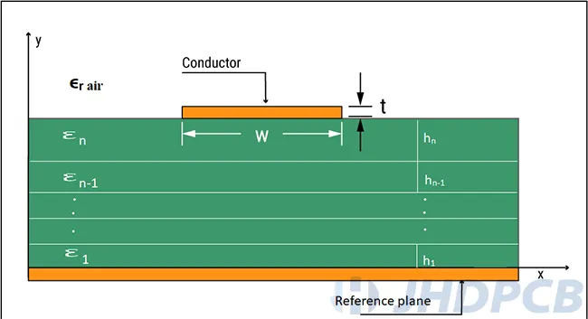
Stripline is a transmission line that is commonly implemented on printed circuit boards. Unlike microstrip, stripline is routed on the PCB internal layer, surrounded by PCB material on all sides. It is typically utilized in multi-layer PCB designs, where the signal trace is sandwiched between two ground planes. The ground planes provide a return path for the high-frequency signal, keeping it confined within the PCB, reducing emissions, and providing shielding against external signals. Due to its structure, strip line provides a controlled impedance environment for signal transmission, resulting in reduced reflections and signal loss. Overall, stripline is a versatile and effective transmission line option for high-frequency and RF applications in PCB designs. Stripline can often be seen on the traces of high-frequency PCBs.
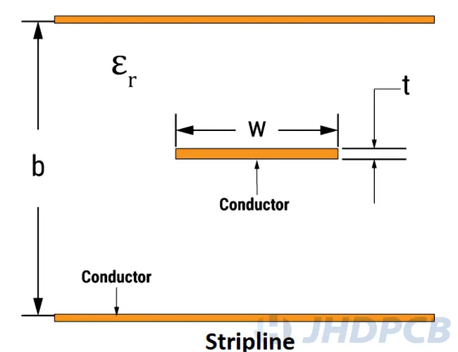
It is composed of a conducting strip placed between two parallel ground planes of conducting material, typically copper, all of which are surrounded by dielectric material (such as FR-4). The trace and planes of the stripline form a controlled impedance transmission line. In terms of structure, the stripline can be described as:
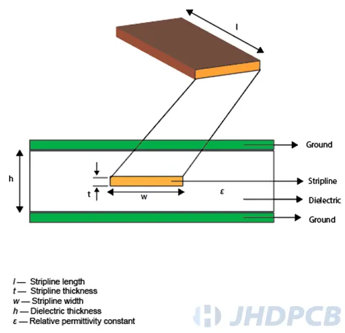
- Conductor strip: The conductor strip, also known as the center conductor, is the primary element of a stripline transmission line. It is typically made of copper and is a thin, flat strip of metal that carries the electrical signal. The width and thickness of the strip is carefully designed to achieve a specific impedance and minimize RF losses.
- Dielectric material: Dielectric material plays an essential role in the operation of stripline. It surrounds the conductor strip and provides insulation between the conductor strip and the reference planes. The dielectric material has a significant impact on the characteristic impedance of the stripline, and its choice depends on the desired impedance, frequency of operation, and other factors.
- Ground planes: They are placed parallel to each other on either side of the conductor strip, providing shielding and grounding to the stripline. The ground planes ensure that external electromagnetic interference does not affect the signal by acting as a shield.
The microstrip impedance, microstrip capacitance, and permittivity of striplines are important parameters that determine their performance and suitability for various applications. By understanding and optimizing these parameters, striplines can be designed to meet specific requirements for applications such as high-speed digital communication, RF and microwave circuits, and power distribution. Below is a concise summary and the equation of each parameter:
Impedance of stripline:
The characteristic impedance of a stripline is determined by the geometry of its center conductor and ground planes, as well as the dielectric constant of the material between them. When the conductor line width (We) increases, the strip line characteristic impedance decreases. Similar to microstrip, there are simplified microstrip equations available to calculate the characteristic impedance of a stripline based on its geometry and dielectric constant. The formula is:
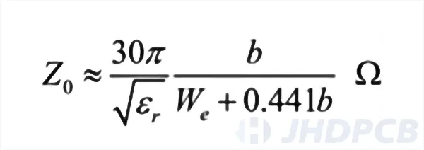
Where:
- Z0 is the characteristic impedance in ohms (Ω);
- b is the spacing between two planes;
- We is the effective strip width.
Characteristic capacitance of a stripline:
The capacitance per unit length of a stripline is dependent on the dielectric material between the strip conductor and the ground planes as well as the geometry of the strip conductor. It can be calculated using the following formula:
Permittivity of striplines:
The relative permittivity, or dielectric constant, of the material surrounding the strip and ground planes is a critical parameter that affects the microstrip capacitance and velocity of propagation of the strip line. Commonly used dielectric materials for striplines include FR-4, Rogers, and Teflon, with relative permittivity values ranging from 2.2 to 10.8. Choosing the appropriate dielectric material is essential for achieving the desired electrical performance of the strip line.
- Microstrip.
Microstrips are transmission lines that are routed on the outer layers of a printed circuit board. They are typically located on the top layer and always routed above a big ground plane on the adjacent layer.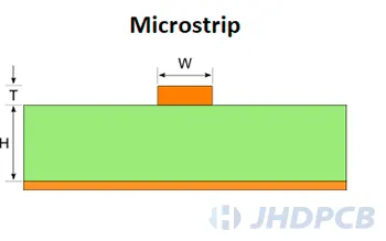
- Edge Coupled Microstrip Line.
This structure is used for routing differential pairs and consists of two microstrip lines that are routed in parallel. It is similar in structure to regular microstrips.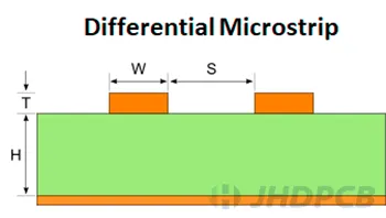
- Symmetric Stripline.
Symmetric stripline is a type of transmission line that is routed on internal layers between two reference planes, with the trace being centrally located between the planes.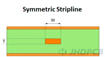
- Asymmetric Stripline.
Unlike a symmetric stripline, this type of trace is not centrally placed between the two ground planes.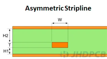
- Edge-Coupled Stripline.
Similar to edge-coupled microstrips, they are also routed in parallel and often utilized as differential pairs. These traces can have either symmetric or asymmetric designs.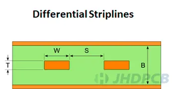
- Broadside-Coupled Stripline.
Like the differential microstrip, the Broadside-Coupled Stripline is a type of differential pair routing configuration where the pair is routed between two ground planes, but not being routed side-by-side, the pair is stacked on top of each other.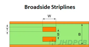
- Embedded Microstrip.
It is uncommon to find embedded microstrips in modern PCBs except in certain HDI PCBs. In this case, as two groups of traces may be put onto the surface two layers, these traces are utilized for slow GPIOs rather than high-speed signals. However, the impedance and loss model for this type of routing could be employed to analyze the impact of soldermask on a microstrip.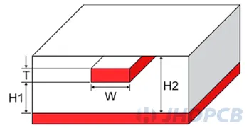
When designing PCBs, each of these transmission lines can be placed in a coplanar configuration with ground poured around the traces to achieve a desired impedance value and provide shielding at certain RF frequencies.
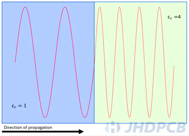
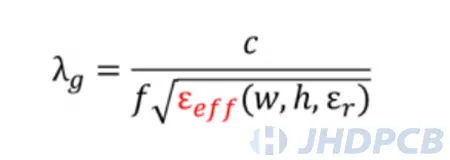
The guided wavelength refers to the wavelength of an electromagnetic signal that is able to propagate efficiently along a microstrip transmission line. A higher dielectric constant results in a shorter guided wavelength and a greater length mismatch between two traces, which causes more propagation delay. For this reason, it is recommended to employ materials with low dielectric constant, which can reduce the effect of propagation delay.
The Wavelength in Microstrip/Stripline Calculator can be utilized to determine the guided wavelength. When use the calculator, put values in the velocity of propagation field and the dielectric constant field. Then requires input the values of the width, height, and the frequency.
Stripline guided wavelength:
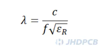
Microstrip guided wavelength:
Note:
Eeff lies on the trace width (w), height between the signal trace and ground layer (h), and Er.
For the same material, the signals travels faster in the microstrip than it does in the stripline.
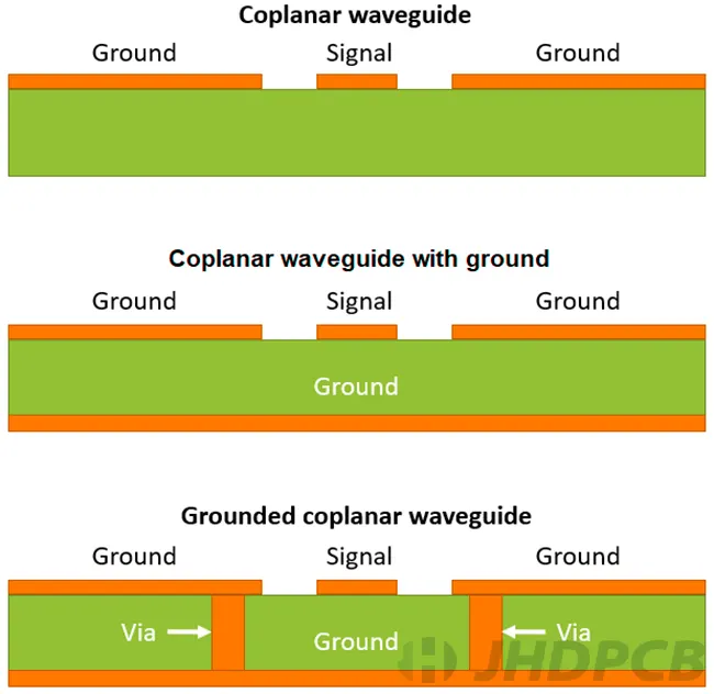
Coplanar waveguide (CPW) is a type of transmission line used in printed circuit board (PCB) design. It consists of a flat conductor strip placed above a ground plane with a small gap between them. Coplanar waveguides are used to transmit microwave frequency signals and high frequency signals. And known for its excellent performance in impedance matching, low insertion loss and high isolation.
In PCB manufacturing, Coplanar waveguide is created by etching a conductor strip on the surface of a substrate, with the ground plane on the opposite side of the substrate. The width of the conductor strip and the gap between the strip and the ground plane determine the characteristic impedance of the CPW. Typical materials used for CPW substrates include FR-4, Rogers, and other high-frequency laminates. On a smaller scale, coplanar waveguide transmission lines are also built into monolithic microwave integrated circuits.
Coplanar waveguide is commonly used in high-speed digital and RF circuits, such as microwave circuits, wireless communication systems, and radar systems. Its advantages include low loss, low dispersion, and easy integration with other types of transmission lines on the same PCB.
In summary, coplanar waveguide is an important component in PCB manufacturing for high-frequency signal transmission, and it has many advantages over other transmission lines. Understanding CPW and its design considerations can help PCB designers and engineers achieve better performance in their electronic circuits.