PCB Stackup

directory

What is PCB stackup?

Prior to board layout design, a PCB’s copper and insulating layers are arranged in a process known as layer stacking. Layer stacking enables you to fit more circuitry on a single board using different PCB layers, but the PCB layer stack design’s structure also has numerous other benefits.

  • When designing high-speed PCB layouts, PCB layer stack-up can help you reduce the amount of radiation, impedance, and crosstalk problems that your circuit is susceptible to.
  • You may also reconcile the necessity for an economical, effective production process with worries about signal integrity problems with the aid of a solid PCB layer stack.
  • Appropriate PCB stack-up layers can help improve the design’s electromagnetic compatibility.

For a multi-layer PCB, typical layers include ground plane (GND plane), power plane (PWR plane) and internal signal plane
Multiple layers increase the board’s ability to distribute energy, reduce crosstalk, eliminate EMI and support high-speed signals. The PCB stackup design has several more benefits in addition to allowing you to have many electronic circuits on a single board thanks to its various levels.
Stacked PCB layers help minimize circuit vulnerability to external noise and minimize radiation and reduce impedance and crosstalk issues in high-speed systems; Good PCB stack-up also contributes to efficient and low-cost finished production; Proper PCB layer stacking might enhance your project’s electromagnetic compatibility.

Board thickness is rarely taken into account for PCBs that are single- or double-layered The stack of materials, however, starts to become increasingly important with the introduction of multilayer PCBs, and eventually cost is the aspect that influences the total project. The simplest stackup can consist of a 4 layer PCB, up to more complex stackups requiring professional sequential lamination. The higher the number of layers, the more freedom the designer has to unravel his circuit and the less chance of getting stuck in an “impossible” solution. PCB overlay operations include the arrangement of copper and insulating layers that make up the circuit. The stackup you choose certainly plays an important role in the performance of your board in several ways.

PCB stackup

Why do you need a PCB stackup?

The popularity of multilayer PCBs is a result of the irreversible development of contemporary electronics, which is increasingly encouraging PCB development toward downsizing, light weight, high speed, greater functionalities and dependability, and longer service life. Designing an effective board requires creating a PCB stackup. PCB stackup has various advantages because of the multilayer structure’s improved energy distribution, reduction of cross-interference, and prevention of electromagnetic interference.
Multilayer PCBs are created by stacking two or more single-sided and/or double-sided PCBs together with a combination of semi-solid adhesives called “prepregs” that are reliable and pre-defined interconnections. even. Multilayer boards have three or more conductive layers, two outer layers, and a composite layer within an insulating board. As PCB complexity and density increase, issues such as noise, stray capacitance, and crosstalk can arise when layer arrangements are designed inefficiently.

One of the most crucial elements in evaluating a product’s electromagnetic compatibility (EMC) performance is planning an ideal multilayer stack.

  • A well-designed stack-up minimizes emissions and protects the circuit from external noise sources.
  • Signal crosstalk and impedance mismatch problems are decreased by a properly layered PCB substrate. However, poor quality stacking increases EMI (electromagnetic interference) emissions, as system reflections and ringing caused by impedance mismatches can significantly degrade product performance and reliability.
  • Lower final production costs can also be ensured with the aid of a solid PCB stackup.
  • PCB stackup can significantly reduce Production time by maximizing efficiency and enhancing the electromagnetic compatibility of the entire project.

How to plan PCB stackup design?

When designing a single- or two-layer PCB, your design is often viewed from a two-dimensional perspective. Nevertheless,the growing demand for smaller, more portable electronics necessitates PCBs that are designed from a multi-layer, three-dimensional perspective. Your design considerations are expanded by this design approach to include concerns like patch packaging and layer stacking. Before we examine how best to create PCB stackups, let’s take a look at how the design perspective for multilayer boards has changed.

The PCB stack-up design perspective includes vertical and horizontal considerations and is a three-dimensional approach that has significant impact on board manufacturing and PCB assembly. The number of layers, their configuration or stacking, and the kind of material must be determined before manufacturing. These alternatives call for a trade-off between thickness restrictions, material characteristics including electrical strength, thermal expansion coefficient, and dielectric constant, signal type isolation, and drilling possibilities. For PCB assembly, it is important to understand routing options and how they affect the soldering process. The alternatives for the vertical component of your design are constrained by this capability of your CM. Now we can look at the best way to achieve a perspective on PCB laminate design.

Important factors to consider when PCB stackup.

Good layering reduces the impedance of the board and limits radiation and crosstalk. Additionally, it has a considerable effect on the product’s EMC performance. A bad stacking design, on the other hand, can greatly increase circuit emissions and noise. When dealing with board stacking, there are four crucial aspects to take into account.

  • The number of layers
  • The number and type of plan used (power plan and ground plan).
  • The ordering and sequence of the levels.
  • The spacing between levels.

Except for those impacting the number of layers, these characteristics are typically not taken into account. Often the fourth factor is not even known to the PCB designer. You should take into account the following considerations when determining the number of layers:

  • The quantity and price of the signals that must be routed.
  • The product’s ability to meet Class A or Class B emission standards;
  • The frequency of operation.
  • Whether the PCB is in a shielded container.
  • Whether the design team is competent in EMC rules and regulations.

All elements should be taken into account equally because they are crucial and vital. The use of multilayer boards with mass and power layers can significantly reduce emissions.When all other parameters are equal, it’s a common rule of thumb that a four-layer board will produce 15 dB less radiation than a two-layer board.

What rules and standards should a quality PCB stackup follow?

Like any other design or product manufacturing, there are some rules that designers need to follow in order to produce the highest quality product. As you know, electronics go through multiple processes involving different components before producing the final product. Therefore, designers must ensure that they identify and follow proven best practices for designing PCB stacks. When it comes to PCB stack design, there are a number of rules that should be followed for best results.

Use of a ground plane is the first guideline. Because they can route signals in stripline, they are the greatest option. Additionally, it plays a vital role in reducing ground noise. Ground noise is significantly reduced due to the reduced ground impedance. Click to view expertise in circuit impedance control.
For high-speed signals, they must be routed to intermediate layers that lie between the different layers. In this way, the ground plane acts as a shield, suppressing the radiation emitted by the orbit at its maximum velocity.
Near the plane is required for the signal layer. Crowd level and power should be carefully linked.
Making sure the configuration is symmetrical is essential. Observe the signal impedance specifications. Each signal layer’s thickness must be taken into account. It’s also important to think about the qualities of the materials that are needed. The thermal, electrical, chemical, and mechanical properties of such materials also require careful consideration.

There are hundreds of rules and standards governing good stackup. Let’s just look at a few:

  1. The first rule is to use a ground plane. They are the most sensible option because of their ability to route signals in stripline. Additionally, it plays a vital role in reducing ground noise. Ground noise is significantly reduced due to the reduced ground impedance.
  2. High-speed signals should be “routed” on intermediate layers located between different layers. . Signal layers should be very close to one another, even in adjacent planes, as this will allow the ground plane to serve as a shield to block radiation from high-speed orbits.
  3. Signal layers should be very close to each other, even in adjacent planes.
  4. Always keep the signal layer close to the plane;
  5. Multiple ground planes are particularly advantageous since they reduce radiation and the board’s ground impedance in a standardized manner;
  6. The power plane and quality plane must be strictly coupled together;

In order to achieve more precise PCB routing goals, the stackup often uses eight layers and above:

  1. From a mechanical standpoint, using a cross-section is advised to prevent distortion;
  2. The arrangement must be symmetrical.. For example, on an eight-layer PCB, if layer 2 is plane, then layer 7 should also be plane;
  3. The return current can flow on the next plane if the signal level is close to the plane’s level (ground or power supply), reducing the return path’s inductance;
  4. The insulation between the signal layer and its adjacent plane can be made thinner to further enhance noise and EMI performance;
  5. The thickness of each signal layer needs to be taken into account, which is a crucial factor. For several kinds of printed circuit materials, there are typical thicknesses and features. It is advised to take into account a material’s electrical, mechanical, and thermal properties while choosing one;
  6. Use excellent software to help you design the stackup. In order to select the appropriate material from the library and execute impedance calculations based on the material and its dimensions, all of this needs be done.

Top 7 tips for PCB lamination design.

Whether it is an HDI or a standard laminate, following certain guidelines depending on the application and its requirements is the best way to implement a PCB laminate design. We have listed some PCB stackup guidelines to help you achieve a possible PCB laminate design.

A) The number of signal layers is important.
The amount of signal layers in the design affects PCB stacking. The signal layers vary depending on the application of the PCB. For example, compared to low speed signal levels, high-power applications or transmissions may necessitate more layers. Complex devices, such as BGAs, with low pitch and high pin counts frequently need extra signal layers. Signal integrity requirements such as very low crosstalk may also lead to an increase in the number of signal layers.
Mixed signal types – A large number of analog and digital signals require separation of the two types and may increase the number of signal layers.

B) Number of ground layers and number of power layers.
In addition to allowing designers to designate signal layers only for signal routing, the usage of ground and power layers lowers the DC resistance in the power and ground rails, resulting in a smaller DC voltage drop on the device. The copper layer of the PCB that is connected to the power supply ground is known as the ground layer. The copper plane in the PCB that links to the power rails is known as the power layer.
Additionally, these planes give time-varying and high-frequency signals signal return pathways, which dramatically lower noise and signal crosstalk and enhance signal integrity. The power supply layer also improves the capacitive decoupling of the circuitry in the PCB. The planes also improve EMC performance by reducing EM emissions.

C) Controlled Impedance Traces.
The characteristic impedance of the transmission line created by the PCB trace and its corresponding reference plane is known as the trace-controlled impedance.When high frequency signals travel via a PCB transmission line, it is important. A homogeneous controlled impedance is important to achieve good signal integrity, which means that the signal propagates without significant distortion.
When the next layer is not the reference plane, a copper feature on the following layer may take on that role.
From a manufacturing point of view, we need to maintain uniform etching over the entire length of the wire, including width and trapezoidal effects. This is where etching tolerances and uniformity come into play.

D) Sequential layer alignment.
The sequential layer arrangement is another essential component of the stack architecture. One of the crucial factors that designers must take into account before routing is how the high speed signal layers should be arranged in relation to the microstrip line thickness.Tight coupling will be possible if the signal layers are positioned below the power plane.
Minimize the space between the power and ground layers to create a precise layer configuration. Avoiding stacking two signal layers adjacent to one another and creating symmetrical stacks of top and bottom layers are additional crucial requirements.
Try to keep the number of lamination processes in sequential lamination to a minimum since it becomes more expensive and time-consuming.

E) Determining the type of layer material.
The thickness of each signal layer is a crucial factor in PCB lamination.Along with defining the prepreg and core material thickness, this should be calculated.There are standard thicknesses and other features for several types of board materials. You should consider these electrical, mechanical, and thermal aspects while choosing PCB materials.

F) Bow and twist.
In multilayer stackups, bow and twist problems could occur if copper is distributed unevenly.Due to this, all multilayer PCBs should be designed symmetrically, with stacked copper weights, symmetrical prepreg thicknesses, and symmetrical corethicknesses.

G) Determining routing and vias.
The selection and routing of the traces completes the PCB stackup design. This includes choosing the sort of vias to use, the location for them, and the copper weights. You should consult your CM when deciding on any specs for your design because certain CMs avoid using particular via kinds, including via-in-pads.

How many structures in PCB stackup design?

The varieties of stacks that are accessible and how to select the best stack design for your needs are crucial concepts to comprehend now that you are aware of the design fundamentals to look for in a PCB multi-layer stack. Two, four, six, eight, and ten layers are the different varieties of PCB layer stacks. The number of layers required is mostly determined by the board’s EMC specifications, board size, and the size of the circuit. From there, You may then determine the board’s layout from there. Below, each sort of board is discussed in further depth along with the circumstances in which it is frequently employed.

One layer of conductive material makes up the 1 Layer PCB stack up, which is ideal for low density and straightforward designs. 2 Layer PCBs contain 2 layers and the layout is easier for more alignments. 2 Layer PCB stackup provides a larger surface area to accommodate conductor patterns. Its surface area is twice that of a one-layer PCB.

A printed circuit board containing four conductive layers—the top layer, two inner layers, and the bottom layer—is referred to as a four-layer PCB. The top and bottom outer layers are utilized for positioning components and signal routing, while the two inner layers, known as the core, are typically employed as power or ground planes.
Surface mount devices and through-hole components can be connected to the outer layer using exposed pads in a solder-resist layer, which is typically used as a placement point. When four layers are fused together to create a board, through-holes are frequently utilized to establish connections between the layers.
The breakdown of these layers is given below.

  • Layer 1: This is the base layer and is usually made of copper.It serves as the foundation for the entire board and gives the other layers support.
  • Layer 2: This is the power supply layer. It is so named because it offers all of the components on the board a stable and clean power supply.
  • Layer 3: This layer serves as the board’s ground source and is known as the ground plane.
  • Layer 4: The top layer is used to route signals and provide connection points for the components.

This is the typical four layer PCB stackup configuration, though it can be changed depending on the design requirements and the layer with the greatest number of signals.

The 4 layer PCB is more versatile and has a wider range of applications than the traditional 2-layer PCB. The additional layers also provide superior thermal management and signal integrity. They are thought to be superior to 2-layer PCBs for these and many more reasons.

A 4-layer board becomes a 6-layer PCB when two more signal layers are put in between the planes. 6-layer PCBs have a standard stack of 4 wiring layers (two outer and two inner layers) and 2 internal planes (one for ground and the other for power). This dramatically increases EMI (electromagnetic interference), which is the energy that destroys signals in electronic equipment through radiation or induction, by offering two inside layers for high-speed signals and two external layers for low-speed signals.

6 layer pcb stackup example

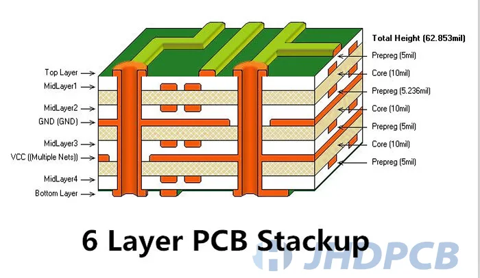
There are several configurations for 6-layer PCB stacks, but the utilization of power, signal, and grounding layers is determined by the needs of the application.
The top layer, internal ground layer, core, internal wiring layer, internal wiring layer prepreg, core, internal power layer prepreg, and bottom layer make up a basic six-layer PCB stackup.
Although standard, this arrangement is not suitable for all layer stackup in PCB designs and therefore may require re-positioning of layers or having more specific layers. However, placement must take into account wiring efficiency and crosstalk minimization.
PCB layer planar spiral coils, hollow inductors inside RF modules for TV receivers, surface-mounted devices.

The 8-Layer PCB has four signal layers and four planes stacked on top of each other. The ground, power, and signal layers are some of these layers. Crosstalk between the signal layers is minimized by the ground and power layers. 8-layer PCBs with stacked layers provide high-quality cabling, enhanced signal routing and increased efficiency in complex compact devices.

8-Layer PCBs also benefit from their high current alignments, which are typically very thick and have low impedance.
They also provide higher EMC (electromagnetic compatibility) performance, higher power and ground plane isolation, and high-speed signal routing.
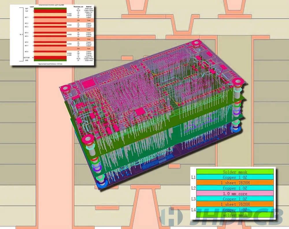
Consider a 10-layer board if your design calls for six wiring layers. Six signal layers, four planes, and a strong connection between the signal and return planes make up a 10-layer PCB stack. A typical 10-layer design is arranged as follows.
Signal Layer 1
Ground plane
Signal layer 2
Signal layer 3
Power plane
Ground plane
Signal layer 4
Signal layer 5
Power plane
Signal Layer 6
For this arrangement, high-speed signals are typically routed on the internal signal layer. If stacked and routed properly, this setup can provide excellent signal integrity and excellent EMC performance. Replacing any ground or power layers with additional signal layers is not recommended, as this can lead to poor performance.

Standard PCB stackup VS HDI PCB stackup.

There are fundamental differences between standard stackups and HDI stackups. For a standard stack up, factors to be aware of include: layer level, number of layers, circuit frequency, and emission requirements. Other parameters related to standard stackups include: space between layers and shielded or unshielded areas.

Still very important are the design rules that are important to standard stackups. The quantity of signal layers determines the standard stack architecture. The number of layers, number of ground and power planes, circuit frequency, order of the layers, and emission requirements are important factors for a typical PCB stack. Some additional parameters include the spacing between layers and shielded or unshielded enclosures.
Maintaining space between signal layers and utilizing large cores to prevent EMC problems are important design principles for standard stacks. It is worth noting that the main advantage of standard stacking is the shielding of the inner layers by the outer layers. At the same time, major disadvantages include reduced ground planes due to the presence of component mounting pads, especially on high-density PCBs.

HDI stacking is a cutting-edge technology that is revolutionizing the design and manufacture of multilayer PCBs. Different from standard stack up, the biggest advantage of HDI is to provide more diverse routing support with more fine hole types. . Also, if you want to simplify the design of complex boards, HDI stackup is the right choice.The quantity of ground and power layers, as well as the number of signal layers, affect stacking. One thing to keep in mind is that the layers ought to be set up symmetrically. The fact that HDI does not require complex architectures is a major advantage for designers.

What differences between rigid and flex PCB layer stackup?

When most people imagine a circuit board, they think of a rigid PCB, often simply called a PCB. These boards use conductive rails and other parts that are arranged on a non-conductive substrate to link electrical components. Glass is frequently included in the non-conductive substrate of rigid circuit boards, giving the board strength and rigidity. A rigid circuit board offers excellent thermal resistance and solid support for the components.
4 Layer flex PCB stackup for a range of industrial uses. For industries like power, automotive, medical, GPS, and industrial control equipment, our PCBs are the top choice. Although flex PCBs can also contain electrical lines on a non-conductive substrate, this type of board uses a flexible substrate like polyimide. The flexible circuit can fold into many forms, tolerate vibration, and dissipate heat thanks to the flexible foundation. Flexible circuits are increasingly utilised in small and cutting-edge electronic goods because of their structural characteristics.
In addition to the underlying substance and rigidity, PCBs and flex circuits differ in the following ways:

  • Production procedure
    Flexible PCB manufacturers utilize an overlay or cover layer procedure in place of solder-resist layers to shield the exposed circuitry.
  • Conductive material
    The strength and thickness of rigid PCBs is usually derived from glass, which is used to reinforce the board. Flexible PCBs employ a more flexible substrate, like polyimide, but do not provide the same amount of strength.
  • Durability
    Although both types of PCBs offer good durability, this durability varies for each. Flexible PCBs are better at absorbing vibration and other shocks while rigid PCBs are stronger.
  • Weight
    Rigid PCBs weigh a little bit more than flexible PCBs, which are frequently lighter due to their strength and thickness. For the electronics sector, which frequently produces smaller gadgets that call for lighter components, this is a useful aspect. Resistance Flexible PCBs provide an advantage over stiff PCBs in harsher situations. Flexible PCBs typically provide a better level of heat resistance. On the other hand, rigid PCBs are more vulnerable to deterioration or warpage.
  • Sophisticated design
    Rigid PCBs frequently function well for less complex consumer electronics, such as toys or musical keyboards. Flexible PCBs, on the other hand, have more intricate designs and are therefore perfect for goods with intricate designs.
  • Typical cost
    Typically, stiff circuit boards are more expensive than flexible circuits. Flex circuits, on the other hand, enable engineers to reduce the size of their products, resulting in indirect cost reductions because of their capacity to fit in small locations.

For more detailed knowledge about flexible PCB, please check our corresponding page.

The Rigid-Flex PCB Difference.

The Rigid Flexible PCB is a circuit board that combines the best features of rigid and flexible PCBs to create a board that is appropriate for a variety of industries. It has the following benefits and makes use of both hard and flexible materials.

  • Versatility
  • Strength
  • Stability
  • Circuit routing density

By combining the flexibility of a flexible PCB with the high strength of a rigid PCB, the rigid-flexible PCB excels in complex applications. This type of PCB is extremely reliable. It also has the advantage of the light weight of a flexible PCB and its small size makes it ideal for situations where space-saving boards are required.
Rigid Flexible PCBs are frequently more expensive than rigid and flexible PCBs because of their many benefits. However, it is ideal when complex products require a cohesive, reliable solution.

When to use rigid and flexible?

Rigid-flex PCB stackup are generally less costly than flexible circuits. I say “generally” because in some applications it may be more affordable to use a flexible PCB than a rigid one, given the total cost of ownership. To get a really accurate picture of total cost of ownership, you first need to welcome the fact that flexible circuits eliminate the need for connectors, harnesses and many other electronic products (PCs and PCs, mixers, powerhouses) drives (solid state drives), horizontal screen TVs and monitors, children’s toys and various electronic devices) In addition, flexible circuits can be found in extremely conservative or potentially elite gadgets, including GPS devices, tablets, PDAs, cameras and wearable devices. PDAs, cameras and wearable devices.
More notably, modernity is not the primary motivation for using flexible circuits. Low-tech applications may use flex circuit innovations from time to time because it makes building simpler.

When to use both?

Now you need to know when to use rigid PCBs and when to use flexible PCBs. Obviously, rigid circuits are not as expensive as flexible circuits. On the other hand, the cost of ownership and the cost of application can determine how much you need to spend. In some cases, using flexible circuits can reduce the costs you incur. If you want to know the full cost of a sole proprietorship, that’s when you should get some reality. Multiple components, such as connectors, wire rope, and other circuit boards, are not required with flexible circuits.
Of course, flex circuits can also be used as integrated PCBs together with rigid-flex POs if required. The ideal strategy might be this one.

If you are unsure whether you should use a rigid PCB or a flex PCB or a rigid-flex circuit board. You can send your design files to our professional engineers for review, and we will give you the most cost-effective and reliable suggestions based on your design application.

JHD can provide PCBs with more layers and special requirements according to the situation.
Multilayer PCB stackups are a great option if you need to add functionality to your PCB. While manufacturing costs and design requirements increase with each layer added, the trade-off in functionality and EMC improvement is easily worth the cost, especially as the world becomes ever more compact. No matter how many layers you require, though, you also need a knowledgeable PCB provider, which JHD can provide.
We continually provide our customers with high-quality printed circuit boards because of our commitment to innovation, quality control, and years of experience. We offer Rigid-Flex, HDI and Laminate boards, as well as many other PCB-related products. You can rely on us to consistently deliver a high-quality pcb board stackup, regardless of the number of layers you require.
Also available from our company is polar pcb stackup, the preferred stackup tool for many high-end manufacturers, value-added brokers, and PCB technologists in OEM bases. used extensively in Europe.

Get a PCB Quote Now

Open high-quality PCB manufacturing services in JHDPCB