PCB Quick Turn

Multi-Layers-PCB

Need a PCB sample urgently?

JHDPCB is your best choice. We have the ability to quickly turn over PCBs, can meet your stringent project deadlines. And provide a free PCB file inspection, combined with the situation to develop appropriate procedures to ensure that your order is expedited throughout the process.

The quick turn to PCB manufacturing and PCB assembly services is the foundation of our business. Our experienced manufacturing team is always ready and willing to make every effort to meet your needs for new product customization, high precision craftsmanship of PCB production process, PCB testing, modeling, etc.

JHDPCB offers rapid PCB prototyping services for quick-turn PCB with high quality and low cost. We’re fully compliant with ISO9001:2008 quality management systems and we have an internal quality control department to verify that all work meets every requirement described by the high standards.

Streamlined processes & Engineering Expertise

We can provide quick turn services because everything is completed under one roof with our own advance equipment. From the first process to the last process of PCB production, it is completed in our own factory. There is no need to seek for outsource. Our own streamlined processes can deliver exactly what you need when you need it.

Our full-service capabilities include:

How Long to Make PCB?

PCB or PCBA manufacturing orders do not have an exact delivery time. The time required for manufacturing is determined by the type of board and the complexity of the process. A qualified PCB/PCBA manufacturer can only speed up the delivery time by perfecting the entire production process and improving the professionalism of its employees. The factors that determine the manufacturing time are as follows:

  • The number of layers of the board – the number of layers of the circuit board;
  • Board Substrate Type – The type of circuit board substrate material, such as aluminum base, copper base, glass fiber board, etc. Click to view detailed substrate information;
  • Number and type of holes on the board – There are different types of holes on the board such as blind holes, buried holes, through holes and tool holes. Different hole types require different process methods, which will consume different time. The greater the number of holes, the longer the time;
  • Order Quantity – The higher the number of circuit board orders, the longer the production time is usually required. But usually large orders will give priority to part of the production;
  • Special processing process requirements – such as special processes such as gold fingers, surface treatment and electroplating;

The lead time represents the time from receipt of an order to delivery of the goods.
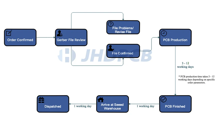
The PCB order processing process is as follows:

  • Receive the order and check the production documents. Avoid large-scale mistakes and unnecessary waste of money – 1 working day;
  • Arrange production. Production will be arranged when the PCB design files are correct and complete production information is available. Click to view the complete manufacturing process – 3~12 working days;
  • Quality check. After the PCB production is completed, a series of electrical tests and environmental tests will be carried out according to the customer’s budget and the application scenario of the board – 1 working day;
  • Packed and shipped – 1 working day;

The PCB order processing process is as follows

The normal lead time for PCB manufacturing is 3-15 working days. It varies according to the PCB order quantity and design parameters. Normal expedited order, if there is no problem with the design file. JHD can be completed within 3~5 days. The detailed PCB fast delivery time is shown in the table below.

The latest delivery time schedule for standard PCB (1&2 -Layer or Multi-layer PCB) orders:
PCB Order Quantity (m2) Original Lead Time (Days) Current Lead Time (Hours)
 < 1m2 2 – 3 Days 24 Hours
1m2 – 5m2 5 – 6 Days 3 – 4 Days
5m2 – 10m2 6 – 7 Days 4 – 5 Days
More than 10m2 8 – 10 Days 5 – 6 Days

We shorten the delivery time while ensuring quality, and fast delivery will never affect quality. Any product must pass the strict quality control system of our professional team, you can rest assured.

The latest delivery time schedule for advanced PCB (HDI PCB)  orders:
Layers PCB Order Quantity (m2) Build Time (Days) Extra Urgent (Hours)
2 Layers

<1 m2

1-5 m2

>5 m2

5 Days

7 Days

8 Days

48 Hours
4 Layers

<1 m2

1-5 m2

>5 m2

5 Days

7 Days

12 Days

48 Hours
6 Layers / 8 Layers

<1 m2

1-5 m2

>5 m2

7 Days

9 Days

12 Days

72 Hours
10 Layers

<1 m2

1-5 m2

>5 m2

10 Days

10 Days

15 Days

96 Hours
10 or more Layers

<1 m2

1-5 m2

>5 m2

10 Days

10 Days

15 Days

96 Hours

Advanced PCBs are often used in high-precision electronic equipment. With the continuous development of technology, the demand is getting higher and higher. To this end, JHDPCB has set up a separate advanced PCB production workshop. Through our advanced manufacturing capabilities, punctual delivery and ultra-high product quality, we can continuously produce PCBs at the lowest price,helping our customers achieve the fastest time to market and competitive advantage.

How Long to Make PCB Assembly?

The lead time for PCB assembly orders is about 7~20 working days. The specific assembly time factors include the following:

  • The manufacturing time of the bare PCB board – the electronic component assembly step can only be carried out after the bare board is manufactured;
  • The number of PCB assemblies – the more circuit boards that need to be assembled, the longer it will take;
  • PCB IC packaging process type – Due to the different application fields of the board, various components and chips need to be used. For different electronic components, the packaging process that needs to be adopted will also be different. Such as: SMT, BGA, Through hole assembly, QFN or mixed assembly, etc. In order to ensure the quality of PCB assembly, different assembly methods require different times;
  • Procurement of components – The electronic components used in PCBA orders are too complex and diverse. Sometimes the factory does not have sufficient inventory and needs to make purchases;

The Process of PCB assembly is as follows:

Usually PCB assembly partners divide assembly orders into OPL orders and non-OPL orders.
OPL Order: On behalf of our component inventory contains the electronic components required for the order. Therefore, the time cost of purchasing components is saved, and OPL orders can be carried out faster and within a controllable range.
Non-OPL Orders: Indicates that some components in the PCB design are not included in our component library. Component procurement needs to be done at the same time as the bare PCB board to save time.

Contact JHDPCB Now

Get the latest PCB project support