Blind & Buried Vias

directory

Comprehensive understanding of through, blind and buried vias.

Common drilling holes in PCBs: through holes, blind holes, and buried holes. JHD will introduce the meaning and characteristics of these three kinds of holes in detail.

VIA

In PCB design, a via is a small opening in an insulating oxide layer that allows conductive connections between different layers. Through holes usually run through the PCB and are used to conduct or connect the copper foil traces between the first and last layers of the circuit board. This is also the simplest kind of hole.
Because the PCB is formed by stacking and accumulating many layers of copper foil, each layer of copper foil will be covered with an insulating layer, so that the copper foil layers cannot communicate with each other, and the signal link depends on the through hole ( via).
The characteristics are: in order to meet the needs of customers, the through holes of the circuit board must be plugged holes. In this way, in the process of changing the traditional aluminum sheet plugging process, white mesh is used to complete the solder mask and plug holes on the circuit board surface, so that the production is stable. Reliable quality and better use. Vias mainly play the role of interconnecting and conducting circuits. With the rapid development of the electronics industry, higher requirements are also placed on the production process and surface mount technology of printed circuit boards. The process of plugging the via hole is applied, and the following requirements should be met:

  1. There is copper in the via hole, and the solder mask can be plugged or not.
  2. There must be tin and lead in the via hole, and there is a certain thickness requirement (4um), and there must be no solder resist ink into the hole, resulting in tin beads hidden in the hole.
  3. The via holes must have solder resist ink plug holes, opaque, and must not have tin circles, tin beads, and leveling requirements.

Click for more detailed through hole information.

Blind Via

Blind via is to connect the outermost circuit in the PCB to the adjacent inner layer with plated holes, that is, the via hole that connects the surface layer and the inner layer without penetrating the whole board. Because you can’t see the opposite side, it’s called “blind pass”. At the same time, in order to increase the space utilization between PCB circuit layers, blind vias are applied.
In the production process, special attention should be paid to the depth of the drilling (Z axis) to be just right, but this method often causes difficulties in electroplating in the hole, so almost no manufacturers have adopted it; it is also possible to connect the circuit layers that need to be connected in advance. Drill holes first, and then glue them together, which requires more precise positioning and alignment devices.

Features: The blind hole is located on one side of the circuit board and has a certain depth for the link between the surface layer and the underlying inner layer. The depth of the hole usually does not exceed a certain ratio (diameter). A relatively large number of interconnect designs are realized in a smaller space.

For example: For example, if there is an 8-layer board, it is necessary to punch holes in the upper 1-layer to 2-layer board to connect the circuit. Layers 8 to 6 are punched to connect the circuit. But the middle 3-5 layers did not break through. This is a blind via, which refers to a via that connects the surface and inner layers without penetrating the entire board.

Buried Via

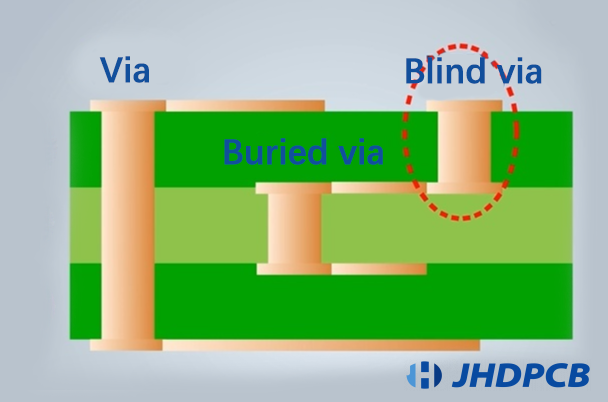
Buried vias: Buried vias only connect the traces between the inner layers. The connection between any circuit layers inside the PCB is not conducted to the outer layer, so it cannot be seen from the surface of the PCB. Generally used in mobile phones and PDA boards. Buried vias can reduce the probability of signal interference, maintain the continuity of the characteristic impedance of the transmission line, and save the wiring space, which is suitable for high-density and high-speed circuit board design. However, the processing cost is also very expensive.

Features: In this process, the method of drilling after bonding cannot be used. Drilling must be performed on individual circuit layers. First, the inner layer is partially bonded and then electroplated. Finally, it can be fully bonded, which is more conductive than the original. Holes and blind holes are more labor-intensive, so the price is also the most expensive. This process is usually only used on high-density circuit boards to increase the usable space for other circuit layers.

For example: For example, there is an 8-layer board, and the circuit design needs to punch holes to connect the circuit between the upper 2-layer to the 7-layer. But the first and last eighth layers of the surface are not perforated. This is a buried via, which refers to the circuit interconnection in the middle layer of a multilayer circuit board without running through the entire board.

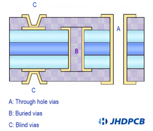
Blind vias and buried vias are only suitable for circuit boards with at least four layers. Unlike conventional through holes on a two-layer board connecting two surface layers, buried holes and blind holes connect the inner layer with other adjacent inner layers or adjacent surface layers.
Vias pass through the entire circuit board and connect all layers. When the surface layer cannot meet all connection requirements, through holes are the solution.

Blind holes are through holes that can be seen from the outside. Their inner layer is connected to the adjacent surface layer (one or more inner layers), and does not pass through the entire board.
Buried vias are vias that cannot be seen from the outside. They are “buried” inside the board and are responsible for connecting two adjacent internal copper layers.

The benefits of blind and buried vias.

The advantage of this technology is that it provides a feasible design technique that helps to meet the density constraints of lines and pads in a typical design without increasing the number of layers or the size of the circuit board.
First, blind vias and buried vias are commonly used in HDI PCBs because they provide excellent power transmission and high-density layers. Blind and buried holes also allow for a larger surface area because they only pass through the necessary layers. They are usually used for fine pitch BGA components.

Secondly, blind and buried vias are often used in multilayer PCBs (usually at least four layers). When plated through holes cannot meet manufacturing and performance requirements, blind and buried vias can help break the density limitations of traces and pads in typical designs.

Third, blind vias and buried vias can increase circuit density without increasing the size and number of layers of the circuit board, thereby making the PCB volume of high-density and high-performance PCB products smaller. These via technologies are more suitable for consumer electronics products.

The disadvantage of this technology is that, due to the additional operations required to manufacture the circuit board, the cost of a circuit board using blind and/or buried vias is significantly higher than that of a typical multilayer circuit board with the same number of layers. Because these vias require more drilling time and additional processes, even so, if you need a high-density PCB with a compact size, don’t forget to add them to your PCB design.
In-depth understanding of how to make blind and buried vias.

In order to better realize blind and buried vias, JHDPCB introduced 18 sets of laser drilling machines from Japan’s Mitsubishi, which can produce PCBs with blind and buried vias quickly and without errors. More details please visit JHD PCB Fabrication.