Thick copper PCB/Heavy Copper PCB

directory

What is Heavy Copper PCB or Thick Copper PCB?

In some real-life high-power applications, ultra-high thermal management compatible with high-power currents is required. Thick copper PCBs are especially good at managing current flow and dealing with special situations. Typically, standard PCBs have copper thicknesses in the 1OZ to 3 OZ range. Heavy copper PCB or thick copper PCB is the type of PCB with finished copper weight between 4oz and 10oz. In some super thick copper PCBs, the copper thickness per square foot may reach 20oz to 200oz. These PCBs are used for high current output and thermal management optimization. Thick copper layers allow large PCB cross-sections for high current loads and facilitate heat dissipation. In electronics applications, temperature management is particularly important. Excessive temperature can seriously damage the performance and life of the circuit board. Using this PCB technology, it is also possible to combine finely laid out structures on the outer layers with thick copper layers on the inner layers.

The width, thickness and purity of copper determine the strength of the PCB, which can make an otherwise fragile circuit board harder and more durable. Of course, the thickness and width of the heavy copper PCB need to be determined according to the impedance and compatibility of the project. This kind of PCB is called heavy copper pcb/ thick copper PCB. These PCBs are used for large current outputs and optimization of thermal management. The thick copper allows large PCB-cross-sections for high current loads and encourages heat dissipation. With this PCB technology it is also possible to combine fine layout structures on the outer layers and thick copper layers in the inner layers. For more PCB design layout information, please click to view.

heavy copper pcb

Construction of Heavy Copper PCB.

A variety of different processes are used in the manufacturing process of heavy copper PCBs to achieve the thick copper requirements of the circuit board.
A combination of etching and electroplating is used in the trace process of a standard printed circuit board. The copper foil is etched to remove unwanted copper and fixed to the board. Additional processes such as planes, pads, traces and electroplating are then added based on the PCB design. (Double-sided or multi-layer circuit boards) Any circuit layers need to be laminated to a complete package using epoxy substrates (eg: cem3, FR4 or polyimide ). Click for comprehensive standard PCB manufacturing process information.

The manufacturing process of thick copper circuit boards is similar to that of standard PCBs. However, special etching and plating techniques are required to ensure that trace sidewalls and undercuts meet thick copper feature standards.
The main manufacturing difficulties include:

  • Etching needs to remove a lot of copper;
  • Etching costs increase;
  • Thin traces are more difficult to manufacture;
  • Thick traces are prone to unevenness;

How to make thick copper PCB?

No matter what manufacturing process a PCB manufacturer adopts, there is one technical difficulty that needs to be faced: solving the problem of uneven thickness of heavy copper PCBs. The manufacturing steps and precautions are as follows:

  1. Use etching to make inner layer traces on each layer of inner core material of the thick copper PCB (note: open a copper-free area at the same position for each layer of inner core material of the thick copper PCB). Reasonably design the pad position. Lay all inner and outer layers together. Do the corresponding electroplating, surface treatment and conformal coating for the surface of the circuit board.
  2. Place an annular ring next to the open area of the core material. All pads are planned to be the same shape and size (shapes include: oval, circle, square and diamond).
  3. The spacing between the pads is uniform. The bottom pad position is the same as the top pad position.

The way of burying copper in the manufacturing process is also different, and the circuit board manufacturer will choose the appropriate method according to the design of the thick copper PCB.
Common heavy copper PCB processes are as follows:

  • Blue Bar: Insert the thick copper bar into the circuit board. This approach reduces the overall weight of the PCB by saving material. The uniformity of the plane is improved by the resin flowing into the space in the copper circuit.
  • Laminate deposition: This process uses a thick base copper. This method is relatively consistent and reliable when placing etch. It is convenient to regulate the edge of the trace and provide fine trace and space.
  • Buried Copper: Insert thick copper into the prepreg in advance. The copper thickness of this method is determined by the resin thickness, using laser cutting.

With the advancement of JHD plating technology, our thick copper plated holes and sidewall copper thickness control have become more and more handy. As a result, impedance control and high-current circuits are integrated to achieve a high-density and more stable circuit structure. We will do custom heavy copper pcb production work according to your project needs.
It is now possible to mix standard circuits with thick copper on a single board to achieve: reduced layer count, area savings, low impedance power distribution and cost savings. Designers need to discuss manufacturing tolerances based on schematics and PCB design drawings to meet project requirements before performing hybrid articulation.

Advantages of Heavy Copper PCBs.

  • Excellent high heat resistance;
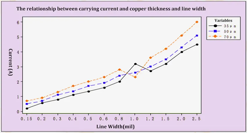
  • Excellent current carrying capacity, It can carry larger current with the same line width;
  • Reduce complex wiring configuration;
  • Compression of board size allows multiple copper weights to be combined on the same PCB;
  • Different copper weights can be incorporated on the same circuit layer;
  • Support the use of special high temperature materials to reduce the circuit failure rate; See more material types.
  • Heavy copper circuits carry taller circuits and transfer heat to external heat sinks;
  • Enhance the mechanical strength of PCB connector area and PTH holes and pads;
  • Improve the elevated current of PCB thick copper plated holes;
  • Integrated high current circuitry and impedance control on a single PCB;
  • Partially plated with heavy copper to provide built-in cooling;
  • The larger the copper thickness, the faster the heat from the components is transferred to the substrate;
  • Reduce the size of end-use products;

Heavy Copper PCB

Ordinary PCB VS Heavy Copper PCB.

Through the above reading of heavy copper PCB, I believe you already know its advantages and characteristics in all aspects. Next, let’s take a look at the difference between standard PCB and heavy copper PCB:

Process: Standard PCBs are made through a series of processes such as etching, hole drilling and electroplating. For thick copper PCBs, finer differential pair etching and step plating processes are required to ensure the goodness of the traces.
Copper weight: The copper content per square foot of a standard PCB is between 1OZ~3oz. In the manufacturing process of thick copper printed boards, the copper content is greater than 3OZ.
Inner layer copper: Standard PCBs have standard definitions for the dielectric constant and copper thickness of the board. But in heavy copper PCB, these factors can be adjusted according to demand.
External Copper: The copper layer on the surface of the PCB facilitates the assembly of electronic components. The same as the inner layer copper, there are standard definitions in standard PCBs. The thick copper PCB can change the weight and thickness of the surface copper to meet the needs of the project.

What is The Difference Detween Copper PCB and Heavy Copper PCB?

Copper pcb and heavy copper pcb seem to have similar names, and people tend to think that the two are the same PCB. But in fact, the two refer to different things. The following JHDPCB will introduce the difference between the copper pcb and heavy copper pcb in detail.

Copper PCB: Copper pcb refers to a copper-based PCB. The use of copper as the substrate is to better dissipate heat and prolong the life of components on the PCB. The copper substrate is to allow the heat to be quickly transferred from the PCB to the outside, such as a heat sink or a metal case, etc. Because the thermal conductivity of copper is several times that of aluminum or other metals, up to 401 W/M.K
Heavy copper PCB: Heavy copper PCB or thick copper PCB refers to the PCB with copper thickness exceeding 3OZ. The substrate can be aluminum, copper can also be fr4. Thick copper is to allow the PCB to carry a large current. Please note that the thick copper mentioned here does not refer to the thickness of the PCB, but the thickness of the copper foil on the PCB. Both aluminum PCB and FR4 PCB can be thickened for copper foil.

What are the characteristics of Heavy Copper PCB?

Due to some unique advantages of heavy copper PCB, it becomes the first choice for some special scenarios and high-end applications. Below we will discuss some of its features:

Ultra-high mechanical strength: After thick copper is applied to the circuit and vias of the board, the printed circuit board has ultra-high mechanical strength. Makes the weather resistance of the circuit board and the electrical system more stable. It can be used in hot melt welding methods such as oxygen blowing at a high melting point and not brittle at low temperatures. Even in extremely corrosive atmospheric environments, copper weight PCB forms a strong, non-toxic passivation protective layer.
Excellent weather resistance: Due to the heavy copper PCB board supports the choice of various dielectric materials. It can ensure the stability of the circuit transmission signal under some high temperature or extreme special environment. Special dielectric materials improve the overall weather resistance of the board.
Thermal Management: With the advancement of modern technology, PCBs are becoming more and more complex. The high density of current increases the difficulty of thermal management. Excessive temperature can affect the normal operation of electronic equipment, and even cause damage. The thick copper PCB board can provide stronger heat dissipation capability. Matching heatsinks and adding copper plating to through holes can drastically reduce board heat.
Excellent current conduction: In the operation of electronic equipment, the heavy copper printed circuit board is an excellent current conductor. It can be connected to transmit electricity between various boards.
Diversity: Its conductive materials, substrate materials, production process, application fields are different from the standard PCBs. The plating of thick copper circuits allows heavy copper PCB manufacturers to increase the copper weight in via sidewalls and plated holes, which can reduce the layer numbers and footprints.
Extendability: Thick copper PCB has the best elongation performance and is not limited by the processing temperature.
High performance: Thick-copper plating integrates high-current and control circuits, making high-density with simple board structures can be achieved.

Thick-copper-PCB2

What is the relationship between current and copper thickness and line width?

We have introduced the thick copper plate above. When do the heavy copper pcb design, the appropriate copper thickness and current should be selected according to the size of the carrying current. So what is the relationship between the current and the copper thickness and line width? The following JHDPCB summarizes a table for reference when designing thick copper pcb.

The amount of current and temperature that a copper PCB can safely carry.
Track Width (inch)
Cu weight (oz/ft2) Thickness (inch) 0.0625 0.1250 0.2500 0.5000 1.0000 2.0000 4.0000 8.0000 16.0000
1 0.0014 4.6 7.6 12.5 20.7 34.2 56.6 93.6 154.7 255.6
2 0.0028 7.6 12.5 20.7 34.2 56.6 93.6 154.7 255.6 422.5
4 0.0056 12.5 20.7 34.2 56.6 93.6 154.7 255.6 422.5 698.4
6 0.0084 16.8 27.8 46.0 76.0 125.5 207.5 343.0 566.9 937.1
8 0.0112 20.7 34.2 56.6 93.6 154.7 255.6 422.5 698.4 1154.4
10 0.0140 24.4 40.3 66.5 110.0 181.8 300.5 496.7 821.1 1357.1
12 0.0168 27.8 46.0 76.0 125.5 207.5 343.0 566.9 937.1 1548.9
14 0.0196 31.1 51.4 84.9 140.4 232.0 383.6 634.0 1047.9 1732.1
16 0.0224 34.2 56.6 93.6 154.7 255.6 422.5 698.4 1154.4 1908.1
18 0.0252 37.3 61.7 101.9 168.4 278.4 460.2 760.7 1257.3 2078.2
20 0.0280 40.3 66.5 110.0 181.8 300.5 496.7 821.1 1357.1 2243.2
24 0.0336 46.0 76.0 125.5 207.5 343.0 343.0 937.1 1548.9 2560.2
28 0.0392 51.4 84.9 140.4 232.0 383.6 634.0 1047.9 1732.1 2863.0
32 0.0448 56.6 93.6 154.7 255.6 422.5 698.4 1154.4 1908.1 3154.0
36 0.0504 61.7 101.9 168.4 278.4 460.2 760.7 1257.3 2078.2 3435.1
40 0.0560 66.5 110.0 181.8 300.5 496.7 821.1 1357.1 2243.2 3707.8
45 0.0630 72.5 119.8 198.0 327.3 541.0 894.3 1478.1 2443.2 4038.3
50 0.0700 78.2 129.3 213.7 353.3 584.0 965.2 1595.5 2637.1 4358.9
55 0.0770 83.8 138.6 229.0 378.6 625.7 1034.3 1709.6 2825.8 4670.8
60 0.0840 147.6 244.0 403.2 666.5 1101.7 1820.9 3009.8 4974.9
70 0.0980 165.0 272.8 450.9 745.3 1231.9 2036.2 3365.7 5563.1
80 0.1120 181.8 300.5 496.7 821.1 1357.1 2243.2 3707.8 6128.6
90 0.1260 198.0 327.3 541.0 894.3 1478.1 2443.2 4038.3 6675.0
100 0.1400 213.7 353.3 584.0 965.2 1595.5 2637.1 4358.9 7204.8
120 0.1680 403.2 666.5 1101.7 1820.9 3009.8 4974.9 8223.0
140 0.1960 450.9 745.3 1231.9 2036.2 3365.7 5563.1 9195.3
160 0.2240 496.7 821.1 1357.1 2243.2 3707.8 6128.6 10130.0
180 0.2520 541.0 894.3 1478.1 2443.2 4038.3 6675.0 11033.1
200 0.2800 584.0 965.2 1595.5 2637.1 4358.9 7204.8 11908.9

After years of accumulation of PCB production technology, JHDPCB can produce th heavy copper pcb with an inner layer copper thickness of 0.5oz-12oz and an outer layer copper thickness of 3oz-20oz. So if you need heavy copper PCB, we will be your reliable partner.

JHD's Heavy Copper PCB manufacturing capabilities.

SequenceSteps
MaterialFR4, High TG, Aluminum, Ceramic, Teflon, Polyimide, Copper
Quality classIPC 2/IPC 3
Thickness of copper4oz-12oz
Extremely heavy copper20oz-200oz
Layers2 – 20 layers
Order quantity1pc – 10000+pcs
Build Time2 – 10 days
Delivery time5 days – 3 weeks
Board sizeMin 6mm x 6mm | Max 500mm x 610mm
Plate thickness0.6mm – 300mm
Max Outer Copper Weight (Finished)20oz
Maximum inner layer copper weight12oz
Type of holeVia/Blind Via/Buried Via
Via CoverageVia Tent / Via Plugging / Via Fill
Surface treatmentENIG/OSP/HASL/IAG/ISN/ENEPIG/ROHS
Minimum Solder Mask Distance6mil
Solder Mask ColorGreen/White/Blue/Black/Red/Yellow/Purple/Matte
Minimum silkscreen line width8mil
Silkscreen ColorWhite/Yellow/Blue/Black/Red
Smallest ring6mil
Minimum drilling diameter10mil
Impedance control+/-10%
Board outlinePunching, Routing, V-Cut

The application of heavy copper PCB.

With the rapid development of science and technology, electronic products are becoming more and more miniaturized. Because the thick copper pcb has the characteristics of being able to carry large current and good heat dissipation. It is suitable for use in electronic products with multiple functions and miniature volume, so the demand for thick copper plates is also increasing.
The application industry areas are as follows:

  • Computer;
  • Solar engineering;
  • Automobile;
  • Railway transportation;
  • Military;
  • Aerospace;
  • Nuclear power;
  • Medical;
  • Industrial control;

Defense military applications are as follows:

  • Weapon control systems;
  • Radar detection systems;
  • Switchboards;
  • Monitoring systems;
  • Security and signaling systems;

Industrial and commercial applications are as follows:

  • High-power transformers;
  • High-power LED lighting;
  • Grid switching systems;
  • Power supplies and power converters;
  • Power conditioners;
  • Torque control;
  • Power equipment;
  • Welding equipment;
  • Overload relays;
  • Protection relays;
  • HVAC systems;
  • UPS systems;
  • Energy storage;
  • Electric vehicle charging systems;
  • Hydropower;
  • Surge protectors;
  • Fuses;

Get a Quote for Custom Thick Copper PCB.

Through the above knowledge, you should have a certain understanding of heavy copper PCB. To know more about heavy copper PCB or the latest heavy copper PCB price, please feel free to contact us. Or upload your Gerber file on our quick quote page. JHD’s professional customer service team will reply you quickly, giving suggestions and preferential prices.