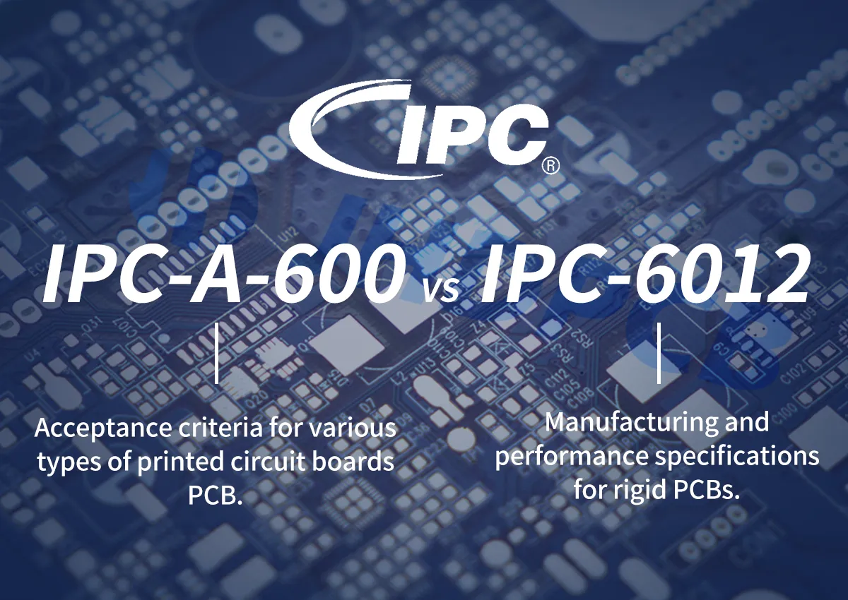
The role of IPC A 600 and IPC 6012 standards in PCB manufacturing

jhdpcb@gmail.com
What is IPC?
The IPC is an industry association whose aim is to standardize requirements for the assembly and production of electronic devices and components. In 1957, the IPC was founded under the name Institute of Printed Circuits. It was later renamed Institute of Electronic Circuit Interconnection and Packaging to reflect the evolution from printed circuits to packaging and electronic components. IPC’s slogan is ‘The association that connects’.
The IPC is a standards development organization recognized by the American National Standards Institute (ANSI) and its standards are known worldwide. In the area of the electronics industry. IPC publishes the most widely used acceptability standard.
IPC confirms the quality of manufactured printed circuit boards and PCBAs by applying a set of inspection guidelines. IPC represents the fundamental elements of the electronics industry, including design, printed circuit board manufacturing, electronic assembly, and final testing. As such, it is a source of industry standards, market research, education, and public advocacy. IPC has established several guidelines for printed circuit board manufacturers to follow when manufacturing printed circuit boards. Currently, IPC-A-600 and IPC-6012 appears to be the most widely used and receivable standard. IPC-6012 deals with the qualification and performance specification of rigid PCBs. The IPC-A-600 standard deals with the acceptance of PCBs. The significance of IPC 6012 and IPC A 600 in the production of PCBs will be emphasized in this article for all of. View more information on IPC standards.
What is the IPC-A-600 standard?
Based on the latest revision of IPC A 600, the IPC-A-600 guideline describes acceptance criteria for circuit boards used by manufacturers and their customers. This standard provides instructions for printed circuit boards and their associated electronic devices to be ideal, reliable and free from defects from the external and internal observable parts. IPC A 600 emphasizes Design for Inspection (DFI), inspection measurements and methods considered early in the product design prototyping phase. To avoid potentially high hidden costs. This standard applies to all types of printed circuit boards such as rigid PCB, metal core, HDI and flexible PCB.
IPC-A-600 describes the minimum requirements that a trained technician can observe from the outside or inside to assess the quality of production. Whether the quality is sufficient depends on the requirements that must be met in operation using the board. IPC-A-600 defines defect tolerances for specific functions of a PCB based on the end use of the board.
The defined scope of the IPC A 600 standard.
The IPC-A-600 standard defines directions to include the following:
- Board thickness;
- Structural integrity of laminates;
- Hole size and characteristics;
- Annular ring features;
- Back drill structure;
- PCB copper features;
- PCB routing;
- Dielectric thickness and imperfections in the solder mask;
- Hole tent and cover padding;
- Etching properties;
- Plating standard;
- Solderability;
- Dielectric removal;
- Wicking;
- Ink marking;
Another IPC-9121 for use with the IPC 600 is a troubleshooting guide document. IPC 9121 lists some common PCB manufacturing problems, their causes, and corrective actions. In addition to this, board designers should also consider the design requirements of IPC-2220 so that customers and manufacturers can agree.
IPC-A-600 Class III standard.
Class 1: General electronics.
Includes products with a limited lifetime and intended for applications where full functionality of the product is an important requirement. These are consumer products, such as games, certain computers, and their peripherals, where surface defects are not relevant and where the main requirement is the functionality of the component.
Class 2: Electronic products for special services.
Category 2 refers to industrial production in general equipment with higher performance and life cycle requirements. Some superficial defects are tolerated.
Class 3: High-end products.
This refers to electronic products that have a consistently high level of functional safety and must perform in accordance with regulations. Malfunctions are not tolerated. Products must function when used. Products intended for use in commercial and military applications where continuous or uninterrupted operational readiness is essential. Circuit boards in this class are used in applications where safety requirements are high and performance is essential. As in medical life support technology, failure is not tolerated.
The designers establish the classification. Higher standards mean that circuit board manufacturers must meet much tighter manufacturing tolerances. There are several reasons why Category 3 production is more expensive. Products in this category require longer operating cycles, on-demand performance and greater reliability and have the most controllable manufacturing tolerances and specifications of the three categories. Cosmetic defects that do not affect electrical or mechanical operation and meet Class 2 criteria do not pass the Class 3 test. Class 3 PCBs are used in industries such as aerospace, high-end medical devices and automotive. The presence of multiple test and inspection points along the production process slows production speed and increases costs. The number of through holes can also significantly slow down the production process, as level 3 requires drums with a 75% vertical fill rate (level 2 requires 50%). If your project must meet Stage 3 requirements, consider extending the delivery time.
What is the IPC-6012 standard?
IPC-6012 is a quality and manufacturing performance specification for rigid printed circuit boards. IPC-A-6012 is a supplement to IPC-6010 and covers all manufacturing processes for rigid printed circuit boards. At the same time, it is also an upgraded version of IPC-A-6011. IPC-A-6011 is a general performance standard and IPC-A-6012 is a more comprehensive rigid PCB specification.
IPC 6012 applies to the following circuit board technologies:
- Single and double-sided circuit board;
- Metal core circuit boards;
- Multilayer board & HDI;
- Active Circuit & Passive Circuit;
Since IPC 6012 is a performance specification, it also states in principle what board suppliers should deliver. Which materials should be used. What tests must be done and how often that test should be done. It depends on the type of device that will later be built with the board and the final application. Regardless of product type such as high TG PCB (high temperature resistance), high frequency PCB (communication or military) or radio frequency PCB (aerospace), it is described in IPC-6012.
The defined scope of the IPC-6012 standard.
- PCB size;
- Dielectric materials and copper foils;
- Trace width and height;
- Plating standard;
- Back drill structure;
- Solderability testing;
- Microporous structure test;
- Surface finish;
- Solder mask specification;
- Ink marking;
- Structural integrity;
- Cleanliness;
- Thermal Stress;
- Thermal shock;
- Mechanical, electrical and environmental parameters;
- Microsection evaluation;
- Quality Assurance Standards;
IPC-6012 has corresponding detailed appendices for different application fields. Such as:
- The IPC-6012EA appendix contains specifications for rigid PCBs used by the automotive industry. These boards are required to withstand rigorous reliability testing criteria (vibration and thermal stress cycling), strictly defined dielectric removal and wicking.
- The IPC-6012ES appendix contains specifications for space and military applications. Covers simulated test conditions where PCBs are subjected to severe thermal cycling, vibration, and space environments.
- The IPC-6012EM appendix contains specifications for medical grade PCBs. It covers finer feature sizes than HDI technology.
What does IPC-6012 regulate in PCB production?
There are many standards in IPC-6012, and below are some of the unique specifications of IPC-6012 worth noting:
Outer Dimension Drawings
Printed circuit boards shall conform to the minimum dimensions specified in IPC-6012 unless otherwise indicated in the specifications or drawings.
Visual
All PCBs must be visually inspected. Visual inspection or final quality control is required prior to product release. Unless otherwise specified, all PCBs shall be visually inspected.
Conductor width and spacing
The width and spacing of the conductors refer to the minimum space between two adjacent copper elements. Generally, conductor spacing and width requirements should be less than 0.007 inches. Anything greater or less than 0.007 inches is inadequate.
Conductor Surfaces
Holes and notches in the voltage plane of Class 2 and 3 printed circuit boards are permitted. However, they shall not exceed 1.0 mm in their longest dimension. In addition, no more than conductive surfaces are permitted on each side.
Purity
IPC-6012 places great emphasis on cleanliness. Therefore, all PCBs must be cleaned before the solder layer is applied. Uncleaned PCBs containing contaminants should not be placed on the market. Cleanliness is required before and after the application of the solder resist.
Plating integrity
Wiring can deteriorate on the PCB hole walls due to precipitation issues. Eventually, the PCB may fail or not function as expected.
Gaps and cracks in laminate
Voids and cracks in laminates are a common problem in PCB manufacturing. A laminate void is the absence of epoxy in an area that should contain epoxy. Cracks in PCBs, on the other hand, can occur at slightly higher stresses during the process.
Such phenomena can be thermal or mechanical in nature. The standard document IPC-6012 specifies procedures to minimise or prevent voids and cracks in laminates.
Hatchbacks
Hatchback is the removal of epoxy from the sidewalls of drilled-through holes. The reason for this is to ensure a good electrical connection between the layers of the PCB.
The IPC-6012 standard requires that the epoxy resin used can be easily removed if necessary. The epoxy material should be easy to remove if it needs to be removed. It is important that the electrical connections between layers are good for signal transmission.
Delamination
Delamination is a defect caused by the material breaking down into layers; IPC-6012 describes measures to prevent delamination. Appropriate materials are required to prevent delamination.
Hole breakouts
A hole breakout is a condition where the bottom does not enclose the hole, either internally or externally. Hole breakout is a problem faced by many manufacturers in the production of printed circuit boards. Hole breakouts can occur both internally and externally on PCBs.
Smear removal
When making printed circuit boards, it is necessary to remove smears. The purpose of smear removal is to remove smears from the walls of the holes to make electrical connections in the inner layers of the circuit.
Removing the smear also ensures that the hole walls adhere adequately; IPC-6012 standards require that the smear be removed before the through hole is plated.
The thickness of the coating
Board thickness is important in the manufacture of printed circuit boards. Consistency plays a major role in printed circuit boards. Board thickness is a necessary standard for printed circuits. There are official standards for board thickness, but there are very common sizes preferred by manufacturers.
Based on the IPC standard for printed circuits, a board thickness of 1.57 mm or about 0.062 inches is preferred. Although today’s PCB designs and fabrications tend to be smaller, PCB thickness remains the most common thickness for almost all formats.
It is more accurate to say that there are now a number of standard PCB sheet thicknesses. These typically include 0.0031 inches (0.78 mm), 0.093 inches (2.36 mm), and 0.062 inches (1.57 mm).
Metal core
The use of metal is to ensure that heat is dissipated from the most critical parts of the board. Important parts are the metal core and the metal heat sinks.
The IPC-6012 standard states that for multi-layer PCBs, the layers must be evenly distributed on both sides of the metal core. For example, in a 14-layer board, the metal core must be placed in the middle layer, which consists of seven layers on the bottom and seven layers on the top layer.
Raised pads
Raised pads can occur on printed circuit boards. Raised sites are the result of a combination of physical and thermal issues. Incorrectly placed pads can cause partial or complete failure of the PCB.
It is normal for the pads to lift when attempting to solder parts or components from the PCB. It can also occur if the connection is stressed to the point that the adhesion between the PCB and the copper is compromised. More PCB pad knowledge can be learned through our corresponding blog;
Foil thickness
For printed circuit boards, the copper foil serves as the base thickness for the copper applied to the inner and outer layers; the IPC standard allows foil thicknesses up to 10% thinner.
The IPC-6012 standard places great emphasis on the thickness of the foil (both inner and outer). Most PCB manufacturers typically use 1/2 oz foil.
| Characteristic | Class 2 | Class 3 | Class 3A* | IPC 6012D/DS RequirementUOS** | |
|---|---|---|---|---|---|
| Annular Ring External PTH | 90° Breakout Accepted Line width to meet Req. | 50 μm [0.00197 in.] min. 20%isolated area reductions due to | 50 μm [0.00197 in.] min. 20% isolated area reductions due todefects permitted. Tear Drops AABUS | Table 3-9 / 3.4.2 | |
| Annular Ring Internal PTH | 90° Breakout Accepted Line width to meet Req. | 25 μm [0.00098 in.] min. | 25 μm [0.00098 in.] min. | Table 3-9 / 3.6.2.1 | |
| Annular Ring, Unsupported Hole | 90° Breakout Accepted Line width to meet Req. | 150 μm [0.00591 in.] min. | 150 μm [0.00591 in.] min. | Table 3-9 / 3.2.4 | |
| Burrs and Nodules | Accepted if minimum hole diameter and copper thickness is met | Table 3-10 | |||
| Bow & Twist | Max. of 0.75% for Surface Mount Boards / 1.5% for all others | 3.4.3 | |||
| Cracks, Laminate | Cracks within and outside not > 80 μm [0.00315 in] | 3.6.2.4 | |||
| Cracks, Barrel / Corner | None Allowed | Table 3-10 | |||
| Cracks, External Foil | Allowed if not extended into plating | Table 3-10 | |||
| Cracks, Internal Foil | None Allowed | Table 3-10 | |||
| Dielectric Thickness/Spacing | 90 μm [0.00354 in.] min. unless specified | 3.6.2.17 | |||
| Lifted land (Visual)/ | None allowed on the delivered (non-stressed) printed board | 3.6.2.10 | |||
| De-wetting Solder Connection areas | 5% Max | 5% Max | None allowed* | 3.5.4.5 | |
| Conductors and planes are permitted | |||||
| Plating Thickness, Copper, Through, Blind, Buried Vias, >2 Layers, Average | 20 μm [0.00079 in.] min. | 25 μm [0.00098 in.] min. | 25 μm [0.00098 in.] min. | 3.6.2.11 Table 3-4 | |
| Plating Thickness, Copper, Through, Blind, Buried Vias, >2 Layers, Thin Areas | 18 μm [0.00071 in.] min. | 20 μm [0.00079 in.] min. | 25 μm [0.00098 in.] min.* | 3.6.2.11 Table 3-4 | |
| Plating Thickness, Copper, Through, Blind, Buried Vias, >2 Layers, Wrap | 5 μm [0.00019 in.] | 12 μm [0.00047 in.] | 12 μm [0.00047 in.] | 3.6.2.11 Table 3-4 | |
| Plating Thickness, Copper, Blind and Buried Microvias, Average | 12 μm [0.00047 in.] min. | 12 μm [0.00047 in.] min. | 20 μm [0.00079 in.] min.* | 3.6.2.11 Table 3-5 | |
| Plating Thickness, Copper, Blind and Buried Microvias, Thin Areas | 10 μm [0.00039 in.] min. | 10 μm [0.00039 in.] min. | 18 μm [0.00071 in.] min.* | 3.6.2.11 Table 3-5 | |
| Plating Thickness, Copper, Blind and Buried Microvias, Wrap | 5 μm [0.00019 in.] | 6 μm [0.00024 in.] | 6 μm [0.00024 in.] | 3.6.2.11 Table 3-5 | |
| Plating Thickness, Copper, Buried Via Cores (2 Layers), Average | 15 μm [0.00059 in.] min. | 15 μm [0.00059 in.] min. | 20 μm [0.00079 in.] min.* | 3.6.2.11 Table 3-6 | |
| Plating Thickness, Copper, Buried Via Cores (2 Layers), Thin Areas | 13 μm [0.00051 in.] min. | 13 μm [0.00051 in.] min. | 18 μm [0.00071 in.] min.* | 3.6.2.11 Table 3-6 | |
| Plating Thickness, Copper, Buried Via Cores (2 Layers), Wrap | 5 μm [0.00019 in.] | 7 μm [0.00027 in.] | 7 μm [0.00027 in.] | 3.6.2.11 Table 3-6 | |
| Nicks and Pinholes, Planes | Max. size is 1.0 mm [0.0394 in] with not more than 4 per side, per 625 sqcm [96.88 sqin] | 3.5.4.1 | |||
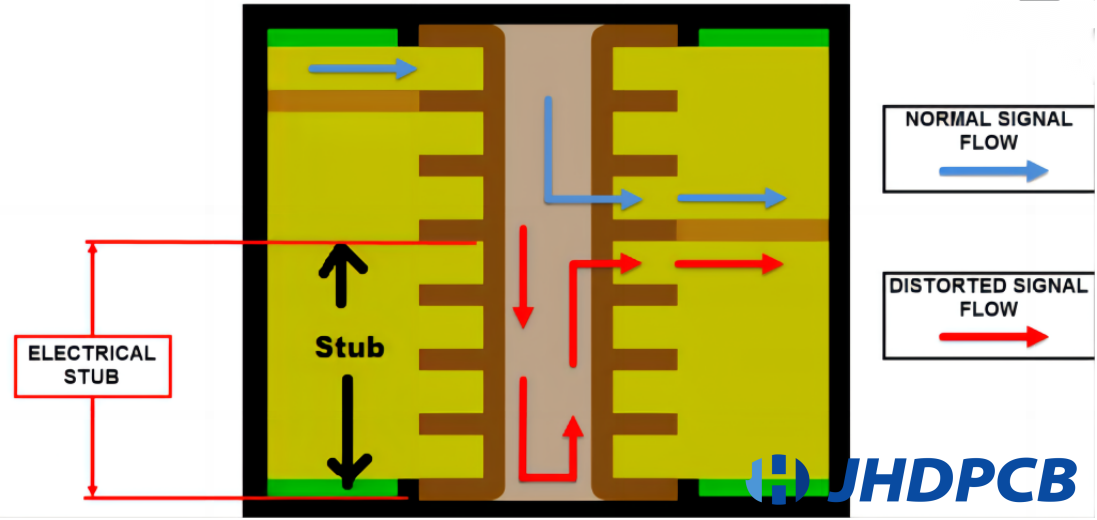
| Negative Etchback | 25 μm [0.00098 in.] | 13 μm [0.00051 in.] | None allowed* | 3.6.2.8 | |
| Positive Etchback | Between 5 μm [0.000197 in.] and 80 μm [0.00315 in.] with preferred depth 13 μm [0.000512 in.] | Between 5 μm [0.000197 in.] and 40 μm [0.001574 in.] with preferred depth 13 μm [0.000512 in.]* | 3.6.2.6 | ||
| The combination of dielectric removal from etchback plus wicking allowance shall not exceed the sum of the maximum allowable etchback or smear removal and the maximum allowable wicking limits in *Table 3-10 and as depicted in Figure 3-15. | |||||
| Surface Mount Lands | Defects along edge of land not > 20%; internal defects not > 10% | 3.5.4.2.1 | |||
| Defects internal to the land remain outside central 80% of the diameter. | |||||
| Plating Separation | None Allowed | Table 3-10 | |||
| Voids, Laminate | Voids within and outside thermal zone not > 80 μm [0.00315 in.] | 3.6.2.3 | |||
| Voids, Copper in Holes (Visual) | One per hole in not more than 5% of the holes | None allowed | None allowed at 3 diopters (approx. 1.75X)* | 3.3.3 Table 3-7 | |
| Voids, Final Finish Plating (Visual) | Three per hole in not more than 5% the holes | One per hole in not more than 5% of the holes | None allowed at 3 diopters (approx. 1.75X)* | 3.3.3 Table 3-7 | |
| Nail Heading | Acceptable – indicator of process variation – alert management | 3.6.2.19 | |||
| Inner layer Inclusions/Separations | None Allowed | Table 3-10 | |||
| Cap Plating of Filled Holes (Visual) | When cap plating of the filled holes is specified on the procurement documentation, plating voids exposing resin are not allowed, unless covered by solder mask. Must maintain structural integrity. | 3.5.4.8 | |||
| Cap Plating of Filled Holes Min. | 5 μm [0.00019 in.] | 12 μm [0.00047 in.] | 12 μm [0.00047 in.] | 3.6.2.11.2 Table 3-11 | |
| Cap Plating of Filled Holes Depression – max. | 127 μm [0.005 in.] | 76 μm [0.0030 in.] | 76 μm [0.0030 in.] general areas 50 μm [0.0020 in.] in BGA areas | 3.6.2.11.2 Table 3-11 | |
| Cap Plating of Filled Holes Protrusion – max. | 50 μm [0.0020 in.] | 50 μm [0.0020 in.] | 50 μm [0.0020 in.] | 3.6.2.11.2 Table 3-11 | |
| Electrodeposited Copper Tensile Strength | > 248 Mpa [36,000 PSI] | > 248 Mpa [36,000 PSI] | > 275.8 Mpa [40,000 PSI] | 3.2.6.2 per IPC-TM-650 2.4.18.1 | |
| Electrodeposited Copper Elongation | > 12% | > 12% | > 18% | 3.2.6.2 per IPC-TM-650 2.4.18.1 | |
| *Requirements for Class 3A product are referenced in IPC-6012DS. | **UOS = Unless Otherwise Stated | ||||
| IPC 6012 Class Chart.doc | For Reference Only | Rev:13-Oct17 | |||
IPC-A-600 vs IPC-6012.
This section describes the differences between IPC-6012 and IPC-A-600 for all of you.
- IPC-A-600 specifies the acceptance criteria for each class specification. It also describes the ideal conditions for PCBs. It is a visual representation of the minimum requirements set for various PCB.
- IPC-6012 is a performance requirements and specifications document. It defines the standard requirements and the specification requirements for each type of PCB. The documents define the requirements for all three PCB classes. However, IPC-A-600 and IPC-6012 are both applying to rigid PCBs.
In a word, IPC 6012 focuses more on the normative standards of the production process, while IPC-A-600 is mostly used for normative testing and acceptance.
How to choose between IPC-A-600 and IPC-6012?
How do you use the IPC-A-600 standard and the IPC-6012 standard? Most PCB designers are a little confused on this point. The most important thing is that the choice between the two depends on the size and requirements of the project. Manufacturers must comply with some overarching test requirements of the IPC standard. The following are the important pointers for choosing between the two standards.
The IPC-A-600 standard plays a very important role in the inspection. It is used exclusively for specifications on printed circuit boards. IPC-6012 specifies the performance specifications and manufacturing standard requirements for rigid printed circuit boards.
If you are a client, it is recommended that you choose the IPC-A-600 standard, based on this standard you can get a good PCB. High-quality PCB manufacturers usually use IPC 6012 as the production specification document when receiving rigid PCB orders, such as JHDPCB.
IPC-A-600 and IPC-6012 are both essential for high-quality PCBs. Both define the characteristics and specifications that PCB manufacturers must meet. Correct understanding of these IPC standards and their combined use play a vital role in PCB design and manufacturing.
What does JHDPCB's A-600 training include?
JHD This training is based on the IPC-A-600 document, which contains inspection criteria for printed circuit boards (PCBs). The PCB produced by JHD will be inspected before leaving the factory to ensure that it meets the requirements and is free of defects. According to IPC-A-600, it is delivered to the customer after a comprehensive inspection from the appearance of the PCB and the invisible parts inside the board. The following is the general content of our training.
- Check connections and printed circuit boards, for example with so-called micro-fetches (sleeves).
- Corresponding AOI, ICT and electrical testing are performed during the board manufacturing process. which checks internally whether the design of the board is compatible and whether there are defects that should not be present on the board. This is to ensure a high-quality product and a compatible product for subsequent assembly. You can click to view JHD’s complete test system.
- In addition, solderability tests and cleanliness tests can be performed to check for the presence of contaminants that should not be present on the PCB and are presented here.
IPC A 600 training is divided into three levels.
IPC-A-600 CIS (IPC Certified IPC Specialist)
This level of IPC-A-600 Certified IPC Specialist (CIS) is designed for operators.
IPC-A-600 CIT (IPC Certified Instructor)
This variant of the IPC-A-600 Certified IPC Trainer (CIT) is aimed at those wishing to train CIS operators.
IPC-A-600 CSE (Certified Standards Expert)
The IPC-A-600 Certified Standards Expert (CSE) is aimed at those who want to become experts in the relevant standards. Companies generally utilise such experts as coordinators to ensure the correct implementation of standards within their company.
Many of them claim that they can produce all types of boards on demand. And almost all PCB manufacturers in the market claim that they comply with IPC-6012 and IPC-A-600 standards. But not all of them can be fully trusted. But JHD can be sure that they comply with IPC-6012 and IPC-A-600 – we all have our requirements for PCBs in IPC-6012.
JHDPCB uses IPC-A-600 as our first inspection specification. If you are interested in our product capabilities, please contact us as soon as possible. If you would like to know more about our quality levels and certifications, it is our honor to introduce them to you.