
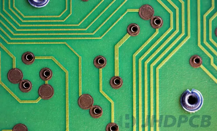
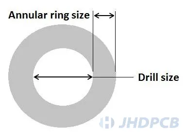
An annular ring in PBC is one kind of the circuit board ring and “annular ring” is a terminology. The reason it is called annular rings is because the formed vias exhibition the shape of ring when seeing from above. According to the annular ring PCB definition, annular rings refer to the area between the hole drilled into a via and the edge of the conductive copper pad in PCBs. We can also understand in this way that annular rings refer to the copper around the via. Annular rings’ dimensions are determined by the dimension of the via and the copper pad.
Now, let’s see the function of annular rings. As we all know, PCBs are multi-layered, vias act as interconnecting nodes between different layers on a PCB. A good connection between the copper traces and the via in a multi-layer PCB can be established by enough copper surrounding this via. Thus,annular rings function as a supplement to enhance the connection between vias and copper traces. In other words, the connectivity is proportional to the thickness of the ring. The thicker the annular, the stronger the connection will be.
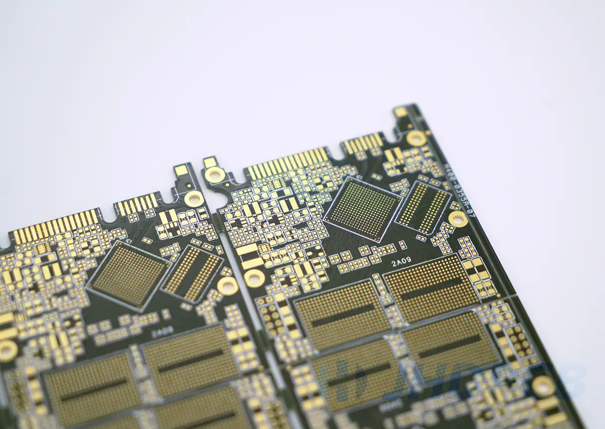
The first thing we all need to know is the PCB annular ring surrounding the via serves as a connection between the copper traces and the different layers of the PCB. In addition to this, annular rings have different sizes and diverse thicknesses. Because of the manufacturing requirements, space constraints, tolerance and other influence factors, some PCB designers will choose the most suitable thickness of PCB annular rings according to these factors above.
When we choosing annular rings, PCB annular ring size should be factored in. The most import point we need to know is that the thicker PCB annular rings can bring us better connection. Thus, the width of annular rings should be thick enough to support a reliable connection with annular ring PCB via. Click to read more detailed PCB hole knowledge. To ensure that things are done smoothly and successfully , people generally use two approaches.
- The first one: the stated width of the annular ring PCB design is less than the minimum value of the annular ring length;
- The second one: Minimum value of the annular ring length is consistent with the stated width of the annular ring.
If the above two practices are not followed, it may cause pad breakout or other connection issues.
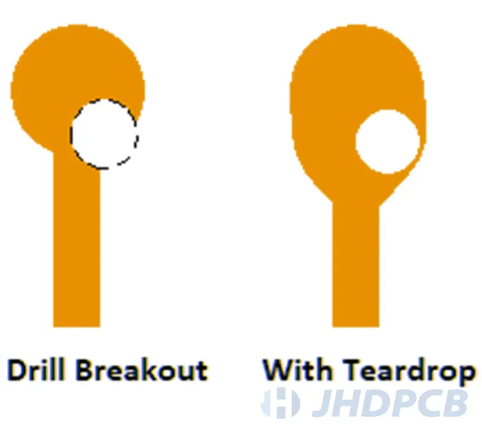
Teardrop annular rings are typical example of adding more copper to improve the connectivity to resist more stress. The working principle of teardrop annular ring is to add further copper around the connection point of the PCB annular rings joined with the PCB traces. The object of this is to gain more stress resistance and more secure and stable connections.
In conclusion, PCB annular ring size is very significant. The thickness of PCB annular rings determines the connectivity. And there exists a positive correlation between them.
- The ideal placement location of via holes is at the dead center of the pad.
In the process of fabricating annular rings, the first tip needing attention is that the via hole must be formed at the dead center of the pad, or the minimum value of the annular rings’ width will definitely exceed the specified value. When a via is misregistered with respect to the land, marginal interconnections may exhibit increased resistance and may be less reliable. - Providing a little more space for annular rings.
An annular ring tolerance will be stipulated by each PCB manufacturer. It is always a good idea to add a little more space to be on the safe side. Increasing 1.0mm of the annular ring PCB size is suggested by most PCB annular ring designers. Having a little extra width will help prevent any future problems.
Depending on what you’re designing the board for, your annular rings will also be different sizes.Three categories for PCB standard(Class1,Class2,Class3)are specified by the Institute of Printed Circuit Boards. Because of the wider diameter of the via, heavy-duty PCBs require larger annular rings. More heavy-duty annular rings are needed for Class 3 PCBs.

A teardrop PCB is teardrop-shaped,which means add more additional copper at the junction of annular rings with traces so as to make the ring possess some added strength.
Applicable situation: During the drilling process, the drill goes slightly off course.
As follow, Teardrop pads can :
- Reduce the stakes of copper cracking;
- Enhance the structural integrity;
- Increase the tolerance in the pad;
- Protect small misalignments in the drill hole.
- IPC-6012 Class 3 Annular Ring Size.
Three classifications are defined by the IPC standards on account of the needed level of equipment reliability, which are Class 1, Class 2 and Class 3. Any one of these classes stipulated its own actual acceptance standard and quality requirement standard for cleaning, fabrication, and inspection of PCBs. Some issues can be resolved in these standards, such as via hole plating, component placement, residual contaminants, trace sizes, and other matters about design aspects. So as to enabling a fabricated plated through-hole via acceptable, we must make sure that there is enough additional space for each annular ring in either class. Therefore, determining the size of annular rings is the process of picking the right size for your via. You can accommodate manufacturing tolerances in your PCB under the condition of having large enough vias. - Annular Rings Visualized.
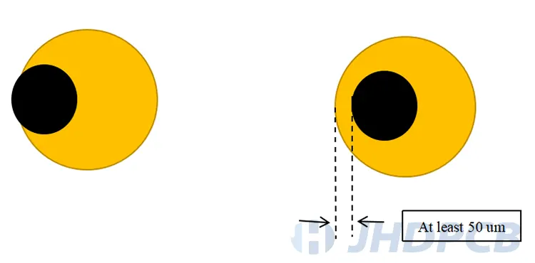
The left diagram below shows breakout, which is accepted under the IPC-6012 standards for Class 1 and Class 2. The right diagram below shows Class 3 annular ring under the IPC-6012 and the forming process of a left annular ring. Under IPC-6012, Class 3 products can be recognized as qualified products when having some leftover annular ring.
| Minimum Annular Ring PCB Size Requirements | |||
| Product Class | External Layers,6012 | Internal Layers,6012 | |
|---|---|---|---|
| Class 1 | Not greater than 180°breakout | Greater than or equal to 20% pad-trace width reduction | |
| Class 2 | Not greater than 90°breakout | 90°breakout accepted | |
| Class 3 | 2 (mil) | 1(mil) | |