PCB Warpage-How to Keep Your PCBs Flat and Functional
PCB warpage is a common issue that occurs during the printed circuit board (PCB) manufacturing process. PCBs are used to connect electronic components and create the necessary electrical pathways for devices to function properly. However, during the manufacturing process, PCBs can become warped or bent, resulting in a PCB warpage.
This warpage can lead to various issues, including component misalignment, poor solder joint quality, and even device failure. In this article, we will delve into the causes of PCB warpage and the methods used to prevent it. By understanding the impact of PCB warpage, manufacturers can ensure the reliability and performance of their electronic devices.
What is PCB Warpage?
Printed circuit boards (PCBs) are a vital component in electronic devices, serving as the foundation or surface support piece for a range of electronic components. PCBs are typically constructed from materials like fiberglass and other composites, depending on their intended use. These boards can be found not only in computers, but also in industrial machines, medical devices, lighting, and many other applications. PCBs come in various types, including single-sided, double-sided, rigid, flexible, and rigid-flex PCBs, as well as microprocessor PCBs used in all types of electronics.
One common issue that occurs during the PCB manufacturing process is warpage, which can cause various problems such as component misalignment, poor solder joint quality, and device failure. PCB warpage is often caused by stress, which occurs during the PCB construction process when the board undergoes expansion and shrinking, leading to internal stress that causes warpage. Temperature changes during fabrication can also cause warpage in the PCB.
To prevent warpage issues, it is essential to analyze the root causes and take preventive measures. PCB warpage has been a significant concern in recent years due to the thin board and thick content of modern PCBs, which can cause construction issues and component failure. The need to address the problem at its early stage is crucial to ensure the reliability and performance of electronic devices.
Indeed, a flat PCB is crucial to retain SMT components in their proper position during reflow. The elevated temperature within the reflow oven can alter the flatness of the PCB, causing SMT components to shift out of position as they float on molten solder. This change in flatness is due to the thermal expansion or contraction of the board materials, resulting in micro-level strains and deformations that can affect the placement of the SMT components. This can cause solder bridging and open circuits, leading to device failure. Therefore, warpage issues need to be addressed early on, and preventive measures need to be taken to ensure the reliability and performance of electronic devices.
To maintain a constant height and proper placement of surface mount technology (SMT), the PCB must be flat in shape. If the PCB has a warpage, it is unable to maintain a constant height, leading to poor solder linking and potential damage to components. Addressing warpage issues early on is crucial in preventing these problems and ensuring the longevity of electronic devices.
What Causes PCB Warpage?
Printed circuit board (PCB) warpage occurs due to several factors during fabrication and processing. The main causes of PCB warpage are:
1.During Lamination
The lamination process is a critical step in the PCB fabrication, where multiple layers of copper and dielectric materials are bonded together under heat and pressure. Warpage can occur during lamination due to:
Thermal mismatch: Different materials used in the PCB stack-up may have different coefficients of thermal expansion (CTE). This can cause uneven expansion and contraction, leading to warpage. Unequal pressure distribution during the lamination process can cause the PCB to warp. The flow of resin between the layers during lamination can lead to uneven thickness and contribute to warpage.
2.During Hot Air Solder Leveling:
During the hot air solder leveling process, the tin furnace is heated to a temperature range of 225℃265℃ for a period of 3S-6S for ordinary board leveling. The hot air temperature is set between 280℃ and 300℃. Also, the board is placed into the tin furnace at room temperature and then subjected to a sudden heating and cooling process during the leveling of the solder.
After solder leveling, the board is removed from the furnace and washed with water at room temperature within two minutes. This process can result in thermal stress due to the different materials and uneven structure of the circuit board, leading to microscopic strain and overall deformation, warping, and distortion.
3.During Solder Mask Curing:
Baking PCBs to cure the solder mask exposes them to temperatures around 150°C which can activate stresses from lamination and cause warpage, especially for PCBs with lower glass transition (Tg) materials. The high elasticity of resins above their Tg point makes PCB components prone to deformation during baking. So, create the glass transition temperature TG with higher values.
4.Improper Handling and Stacking:
Mishandling PCBs during processing and storage can apply mechanical stresses that cause warpage. The way PCBs are stacked and clamped during storage and transportation can also subject them to mechanical stresses if not done properly. These stresses are especially problematic for thinner PCBs.
5. Imbalanced Copper Distribution:
The percentage of copper in each layer and overall copper layers balance in the PCB determines how much it will expand and contract during heating and cooling, which drives warp pcb. Too much copper on one side of a PCB compared to the other can lead to uneven expansion and increased warpage. Proper copper balancing during design helps minimize this.
6.Material Incompatibility:
7.Improper process controls:
Uneven heating or excessively long heating during fabrication can exacerbate warpage by activating more stresses in the PCB. Fabricators must carefully control process temperatures and times to minimize this. Even heating both sides of a PCB helps reduce temperature gradients that can drive warpage.
Also to cure the solder mask inks, the PCB boards are baked in a rack to ensure that the inks do not overlap during the curing process. The temperature used for the solder mask typically reaches around 150°C, which exceeds the Tg point for medium and low Tg materials. At this temperature, the resin becomes highly elastic, making the boards vulnerable to deformation under their own weight or the strong winds generated by the oven.
8.Storage Conditions:
9.Board Size and Number of Panels:
10.V-Cut divider for the router:
V-cut dividers are often used to separate the panels of a PCB after assembly. However, these dividers can weaken the structural integrity of the board and increase the risk of warpage.
Overall, PCB warpage is the result of thermal and mechanical stresses generated during fabrication and processing. Maintaining proper design, material selection, process controls, and handling procedures can help minimize warpage and produce high-quality PCBs. With careful optimization, warpage can often be reduced to within acceptable industry standards.
The Hazard of PCB Warping and Common Deformation Types
PCB warpage causes a number of issues in electronic devices, leading to reduced performance, reliability problems, and in severe cases complete failure. The following are potential hazards of PCB warpage:
Physical Damage:
Highly warped PCBs can experience physical damage during the assembly process or operation. Components may get knocked loose from their solder joints. Flexing of the PCB over time can cause fatigue failure of solder joints, traces, and even the PCB laminate itself.
Poor Component Contact:
When components are soldered to a warped PCB, they may lose full mechanical and electrical contact with the PCB. This can impact performance, increase resistance in electrical connections, and lead to overheating of solder joints over time.
Electromagnetic Interference:
The air gap created by a warped PCB can allow electromagnetic interference (EMI) to affect circuit performance. Components may experience reduced immunity to EMI from external sources.
Impeded Airflow:
For PCBs used in applications with forced convection cooling (fans), significant warpage can block or redirect airflow, reducing the ability of heatsinks and other cooling elements to dissipate heat from components. This can lead to overheating and component damage/failure.
Impeded Mating Connections:
Warped PCBs may not mate properly with connectors, cables, switches, and other mating components. This can impact the reliability of those connections and the overall system.
Stress on Components:
Excessive PCB warpage can place mechanical stress on components soldered to the PCB, particularly BGA and QFN packages. This stress can cause premature failure of solder joints over time.
Common Deformation Types of PCB
There are several common deformation types that can occur in printed circuit boards (PCBs), including:
1.Bowing:Bowing refers to a deformation of the PCB in which the board curves or bends along its length. This type of deformation can occur due to uneven stress distribution during manufacturing or temperature changes during operation.
2.Bowl:This deformation has a sunken middle section, resembling a bowl. It can occur due to uneven stress distribution during manufacturing or temperature changes during operation.
3.Twisting:Twisting refers to a deformation of the PCB in which the board rotates around its axis. This type of deformation can occur due to uneven stress distribution during manufacturing or due to mechanical stress during handling or installation. Overall, we can say both PCB Bow and Twist happened due to stress.
4.Arch:An arch deformation is the opposite of a bowl, having a curved, elevated mid-section. This type of deformation can occur due to uneven stress distribution during manufacturing or temperature changes during operation.
5.Saddle:This deformation has a sunken mid-section extending across the horizontal plane. It can occur due to uneven stress distribution during manufacturing or temperature changes during operation.
6.Delamination:Delamination refers to a separation of the layers in a PCB. This type of deformation can occur due to moisture absorption, thermal stress, or mechanical stress during handling or installation.
7.Cracking:Cracking refers to a fracture in the PCB. This type of deformation can occur due to mechanical stress during handling or installation, or temperature changes during operation.
PCB warpage is a major concern in automated surface mount lines as it can lead to inaccurate component positioning, prevent proper insertion or mounting of components on the holes and surface mount pads of the board, and even damage automatic insertion machines. These issues can result in reduced product quality, lower production yield, increased manufacturing costs, and delays in product delivery. After soldering, a bent circuit board can make it difficult to cut component feet neatly, and the board may not fit correctly in the chassis or socket inside the machine, causing annoyance for assembly plants.
With the advancement of surface mount technology towards precision, speed, and intelligence, PCBs accommodating various components are required to meet increasingly higher flatness standards. According to IPC standards, PCBs with surface mount devices can have a maximum allowable warpage deformation of 0.75%, while those without surface mounting can have a maximum allowable deformation of 1.5%. These standards highlight the importance of maintaining PCB flatness to ensure the reliable and effective functioning of electronic devices, especially in high-performance applications. Therefore, PCB manufacturers are focusing on developing effective strategies to minimize warpage and meet these demanding industry standards. However, some electronic assembly manufacturers have even stricter requirements on the amount of warpage, with some requiring as low as 0.3%.
PCBs are composed of copper foil, resin, glass cloth, and other materials, each with different physical and chemical properties. When pressed together, thermal stress can occur, causing warpage. Additionally, the PCB processing process involves various steps, including high temperature, mechanical cutting, wet processing, etc., all of which can have a significant impact on the PCB Board warpage.
The causes of PCB warpage are diverse and complex, making it a challenging issue for manufacturers to address. Material characteristics, processing methods, and design can all contribute to warpage. To reduce or eliminate warpage, manufacturers need to implement effective strategies such as selecting appropriate materials, optimizing the manufacturing process, and improving PCB design. By taking a comprehensive approach, manufacturers can improve the quality and performance of their products and meet the needs of their customers. It is essential to take preventive measures to ensure the reliability and performance of electronic devices and prevent potential hazards caused by PCB warpage.
How to Measure Warpage in PCB?
There are a few common ways to measure warpage in PCBs:
Direct Measurement Techniques
Here we will discuss 5 methods that can be used to measure PCB Warpage in direct measurement technique.
Method 1: Feeler Gauge Method:
Method 2: Height Gauge:
A mechanical or digital height gauge can be used to accurately measure the difference in height between the high and low points of a warped PCB. This gives you an exact measurement of the warpage in inches or millimeters.
Method 3: Contour Gauge:
A contour gauge uses a stylus to trace the profile of a warped PCB and displays the measurements on a readout. This gives you a complete mapping of the PCBs shape and all high and low points.
Method 4: Optical Profilometer:
An optical profilometer projects a light pattern onto the PCB and uses a camera to capture an image. The software then analyzes the image and generates a 3D profile map of the PCB’s surface. This provides the most precise measurements of the PCB warpage.
Method 5:Finite element method (FEM)
This study proposes a novel method for measuring the warpage of printed circuit boards (PCBs) during the reflow process using strain gauges. The researchers conducted experiments on a bi-material plate and a PCB with DIMM sockets by using a full-field shadow moiré to measure the out-of-plane deformations (or warpage) during solder reflow heating. To validate their results, they also used a finite element method (FEM) to analyze the thermally-induced deformation of both specimens. During the solder reflow process, conventional strain gauges were used to measure the strains in both specimens, although they could only provide in-plane strain data.
Results demonstrated that bending strains occurring during the solder reflow process on the top and bottom surfaces of the PCB could be determined from the in-plane strain data collected by the strain gauges. These bending strains were then converted into curvature data and global warpage, which were found to be consistent with the results obtained through shadow moiré and FEM. This confirms that strain gauge measurement can be used as a real-time and simple method for monitoring PCB warpage with temperature variation during the reflow process.
In general, the higher the precision of the measuring tool, the better. Feel gauge methods are good for a rough estimate, while contour gauges, profilometers, and bake tests provide the most accurate warpage measurements. Measurements should typically be taken at multiple points across the PCB to identify high and low spots.
PCB Warpage Measurements Types:
There are different methods available to pcb warpage calculation of a printed circuit board (PCB), depending on the specific requirements of the application. Three possible measurement types are:
1) The warpage measurement of the entire PCB area
This involves obtaining the height data of the entire PCB area to determine the overall warpage of the board. This method can provide a general assessment of the PCB’s warpage, but it may not be suitable for identifying specific areas with higher levels of deformation.
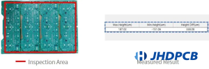
2) The warpage measurement of specific PCB area
This method requires setting up a specific area for measurement, allowing for a more detailed and precise analysis of the warpage at that particular location. This type of measurement is useful for identifying specific areas of the PCB that may require additional attention or adjustments.

3) The measurement of warpage of individual circuits on a panel
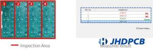
To determine the warpage of specific circuits on a PCB panel, it is essential to measure the deformation that occurs above the maximum height allowance in those particular modules. By analyzing the warpage of individual circuits, it is possible to identify areas that may be more prone to failure or defects. This type of measurement is particularly important in applications where high reliability is required, such as in aerospace or medical devices.
IPC Standard for PCB Warpage
There are IPC standards that specify acceptable PCB warpage level. The relevant IPC standards are:
IPC-6011: Generic Performance Specification for Printed Circuit Boards
IPC-6012: Qualification and Performance Specification for Rigid Printed Boards
These standards define various “classes” based on performance requirements. For PC Warpage, the classes are:
Class 1: Least restrictive, allowing up to 0.2% (0.2 mm per 100 mm) of PCB length warpage
Class 2: Allows up to 0.15% of PCB length warpage
Class 3: Allows up to 0.1% of PCB length warpage
Class 4: Most restrictive, allows up to 0.05% of PCB length warpage
For example, a 400 mm long PCB would be considered:
Class 1 if it warped up to 0.8 mm
Class 2 if it warped up to 0.6 mm
Class 3 if it warped up to 0.4 mm
Class 4 if it warped up to 0.2 mm
Warpage is measured on a flat surface and refers to the maximum difference in height from the lowest point to the highest point over the board’s length.
So according to IPC standards:
Up to 0.2% warpage is acceptable for general-purpose boards (Class 1)
0.1% or less warpage is recommended for higher reliability applications (Class 3 or 4)
Manufacturers should specify the required IPC class for their PCBs based on the intended application and reliability requirements. The standard then provides an objective measurement for suppliers to comply with.
How to Prevent PCB Warping and Deformation?
Printed circuit board (PCB) warpage is a critical issue during the production process that can greatly affect the quality of the final product. After soldering, boards with components may become bent, making it difficult to neatly align component feet. This can prevent the board from being installed properly on the chassis or socket inside the machine, ultimately impacting the normal operation of the entire subsequent process.
1.Engineering design:
With the rise of surface mounting and chip mounting, the demands for PCB warpage control have become increasingly stringent. As a result, it is essential to identify the root causes of warpage to ensure the successful production of high-quality PCBs.
To prevent warping, it is essential to ensure symmetrical arrangement of interlayer prepregs. For example, in a six-layer board, the thickness between layers 1-2 and 5-6 should be the same, along with the number of prepregs. It is also recommended to use products from the same supplier for both multi-layer core boards and prepregs to ensure uniformity in material properties. Furthermore, the area of the circuit pattern on both side A and side B of the outer layer should be as similar as possible.
When designing the board, special attention should be paid to the balance of copper areas and lines on each side to prevent warpage. A large copper surface on one side and only a few lines on the other side can cause the board to warp after etching. Therefore, it is recommended to add independent grids on the thinner side for balance.
2.Baking Board Before Cutting:
Baking the board before cutting or after cutting can help prevent warpage. To remove moisture, solidify the resin, and eliminate stress in the board, it is recommended to bake the board at 150 degrees Celsius for 8±2 hours before cutting the copper clad laminate. Baking the board after cutting can help ensure consistency in board thickness, and it is also advisable to bake the inner board. Different PCB factories use varying drying times, typically ranging from 4 to 10 hours.
The appropriate drying time depends on factors such as the grade of the printed board produced and the customer’s requirements for warpage. By taking these factors into account, manufacturers can determine the optimal drying time to ensure the reliable and consistent performance of the printed circuit board.
3.The Latitude and Longitude of the Prepreg:
The latitude and longitude of the prepreg are critical factors in preventing warpage of the finished board. After lamination, the warp and weft shrinkage rates may differ, so it’s crucial to distinguish the warp and weft directions during blanking and lamination.
By doing so, manufacturers can ensure that the prepreg is aligned correctly, which minimizes the risk of warping and enhances the reliability and performance of the printed circuit board. Proper alignment of the prepreg also helps to optimize the manufacturing process, reduce production defects, and lower manufacturing costs.
One of the leading causes of warpage in multilayer boards is the haphazard stacking of prepregs without distinguishing their warp and weft directions during lamination.
To differentiate between the latitude and longitude of the prepreg, the warp direction is considered to be the rolling direction of the rolled prepreg, while the width direction is the weft direction. For copper foil boards, the weft direction is considered to be the long side, and the warp direction is the short side. If there is any uncertainty, it is advisable to check with the manufacturer or supplier for proper guidance.
4.Stress relief after lamination:
Stress relief after lamination is critical to prevent the warpage of the final board. After the multi-layer board is hot-pressed and cold-pressed, it should be removed from the press and have any burrs cut or milled off. It should then be placed flat in an oven at 150 degrees Celsius for four hours. This process allows for the gradual release of stress in the board while fully curing the resin. This step is critical and cannot be skipped to ensure that the board is reliable and performs correctly.
5.The thin plate Needs to be Straightened During Electroplating:
To prevent warping during electroplating, it is crucial to straighten the thin plate beforehand. For ultra-thin multi-layer boards with a thickness of 0.4 to 0.6mm used for surface and pattern electroplating, manufacturers should create special clamping rollers. After clamping the thin plate onto the flyby of the automatic electroplating line, a round stick is used to clamp the entire flybus, and the rollers are strung together to straighten all the plates on the rollers.
This step ensures that the plates will not be deformed after plating. Without this crucial step, the PCB may bend after plating a copper layer of 20 to 30 microns, which is difficult to remedy. Therefore, it is essential to implement this process to prevent warping of the finished board and ensure reliable and consistent performance.
6.Cooling of the Board After Hot Air Leveling:
Proper cooling is essential to prevent warpage after hot air leveling of printed circuit boards. During hot air leveling, the board is subjected to high temperatures of approximately 250 degrees Celsius. To prevent warpage, the board should be placed on a flat marble or steel plate for natural cooling after being removed from the hot air leveling machine. This step is crucial before sending the board to a post-processing machine for cleaning.
Some factories may opt to cool boards immediately after hot air leveling by submerging them in cold water to enhance the brightness of the lead-tin surface. However, this practice may cause warping on certain types of boards, leading to twisting, layering, or blistering. To prevent this, manufacturers can install an air flotation bed on the equipment for cooling instead of using cold water. By implementing proper cooling techniques, manufacturers can ensure the reliable and consistent performance of the printed circuit board.
7.Treatment of Warped Board:
Treatment of warped boards is necessary to salvage them. In a well-managed printed circuit board factory, it is standard practice to perform 100% flatness checks during the final inspection. Any boards that do not meet the required standards are identified and then placed in an oven.
They are then baked at 150 degrees Celsius under heavy pressure for 3-6 hours and allowed to cool naturally under pressure. After the pressure is relieved, the board is checked again for flatness. Some boards may require multiple rounds of baking and pressing before they can be leveled. Without implementing the anti-warping process measures mentioned above, some boards may be rendered useless and can only be scrapped.
8.Flatness Check During Final Inspection:
A 100% flatness check during the final inspection is critical to ensure that all boards that do not meet the required flatness specifications are identified and treated appropriately. Any unqualified boards should be placed in an oven, baked at 150 degrees Celsius under heavy pressure for 3-6 hours, and cooled naturally under heavy pressure. Baking the board under heavy pressure helps to flatten any warped boards, salvaging them and preventing waste.
9.Proper Handling During Electroplating:
Special clamping rollers should be made for ultra-thin multi-layer boards to prevent warping during electroplating. During electroplating, the high temperature of the plating bath (around 250 degrees Celsius) can cause the plates to deform. To prevent warping, it is crucial to straighten all the plates during electroplating. This can be achieved by using special clamping rollers, which ensure that the plates remain straight and do not deform after plating.
10.Proper Design:
A symmetrical arrangement of interlayer prepregs is essential to prevent PCB warping. To ensure a balance of copper surfaces and lines on each side of the board, it is essential to arrange the prepregs symmetrically. Additionally, the area of the circuit pattern on both sides of the outer layer should be as similar as possible. Distinguishing the latitude and longitude of the prepreg helps ensure that the warp and weft shrinkage rates are equal, preventing warping. Stress relief after lamination is also critical to gradually release the stress in the board and fully cure the resin, preventing warping.
11.Reduce the board size and number of panels:
When using back weld furnaces to drive printed circuit boards, chains are typically used to move the boards through the furnace. However, large PCBs with broad sections hanging between the chains can pose a higher risk of warping due to the weight distribution. To minimize this risk, it is recommended to reduce the board size or use the long side as the edge on the chain if the board is rectangular. This helps to distribute the weight of the board more evenly and reduce the risk of deformation.
12.Use a tray jig or reflow carrier:
If it is not possible to reduce the PCB size, the alternative is to use a tray jig or reflow carrier for support during the soldering process. These tools can help to keep the board flat and prevent it from warping during the heating and cooling cycles of the reflow process.
13.Ditch the V-Cut divider for the router:
V-cut dividers are often used to separate the panels of a PCB after assembly. However, these dividers can weaken the structural integrity of the board and increase the risk of warpage. Instead, it is recommended to use a router to separate the panels. This method is more precise and does not damage the board’s structural integrity.
How to Fix PCB Warping?
PCB warpage is a common issue in the manufacturing process, and preventing it from happening is crucial. There are several methods that PCB manufacturers can employ to avoid or fix PCB warpage.
Designing Around Warpage:
One of the most effective ways to prevent PCB warpage specification is to design the printed circuit board with potential warpage in mind. A well-balanced design is essential to reduce the amount of warpage that occurs. The symmetry of the board is critical, and PCB designers need to ensure that the layers of a multilayer printed circuit board are balanced.
Also, the thickness of the layers should be symmetrical along the center of the board to prevent warpage. Using the same supplier for prepregs and core sheets can also help ensure the coefficient of expansion is similar and prevent warpage. Moreover, the outermost layers on both sides of the board should match each other to ensure that copper pouring areas on both sides have similar thicknesses, preventing warpage.
Pallets and Fixtures:
When using back weld furnaces to drive printed circuit boards, chains are typically used to move the boards through the furnace. However, large PCBs with broad sections hanging between the chains can pose a higher risk of warping due to the weight distribution.
To minimize this risk, it is recommended to reduce the board size or use the long side as the edge on the chain if the board is rectangular. This helps to distribute the weight of the board more evenly and reduce the risk of deformation.
Plate Flattening:
Some manufacturers use specialized machines to flatten out boards that deviate too far from the norm. These machines are typically used at certain points during the manufacturing process, and their effectiveness at flattening the board is often limited. Warpage can rebound after the flattening process, and the results may not be satisfactory.
Addressing Environmental Factors:
Environmental factors can contribute to PCB warpage. Improper storage of substrates can lead to an increased risk of warpage. Copper-clad laminates can absorb moisture, especially in environments with high humidity. Moisture-proof packaging can help reduce the risk of warpage. Additionally, heavy objects pressing down on plating can increase warpage overall. Therefore, it is essential to monitor storage conditions in advance and minimize humidity in warehouses.
Thermal Management:
Thermal management is crucial in preventing PCB warpage. Appropriate baking and drying of the board, both before and after lamination, can help remove moisture, make the resin in the board solidify, and eliminate remaining stress in the board, preventing warpage. Proper handling during electroplating, such as using special clamping rollers for ultra-thin multi-layer boards, can also prevent warpage. Natural cooling of the board on a flat marble or steel plate after hot air leveling can help cool the board evenly, preventing warpage.
So, preventing PCB warpage requires a combination of proper design, thermal management, and addressing environmental factors. By incorporating a balanced design, appropriate thermal management, and monitoring storage conditions, manufacturers can reduce the risk of PCB warpage and produce high-quality boards. While plate flattening and pallets and fixtures can mitigate warpage to some extent, they should not be relied on solely to prevent warpage.
PCB warpage is a common issue in the manufacturing process, and it can lead to significant problems. However, by employing proper design techniques, thermal management, and addressing environmental factors, manufacturers can reduce the risk of PCB warpage and produce high-quality boards.
At JHDPCB, we understand the importance of producing flat and functional PCBs. As a reliable manufacturer, we utilize the latest techniques and technologies to ensure that our PCBs meet the highest quality PCB warpage standards. We pay close attention to the design phase, thermal management, and storage conditions to prevent warpage from occurring. Our experienced team of engineers and technicians is dedicated to producing high-quality PCBs that meet the needs of our clients.If you are looking for a reliable PCB manufacturer that can provide you with high-quality PCBs that are free from warpage, look no further than JHDPCB. We are committed to providing our clients with the best possible PCBs, and we strive to exceed their expectations in every aspect of our service.