thermoelectric separation

PCB Copper substrate with Thermoelectric Separation

directory

What is Thermoelectric separation?

Thermoelectric separation substrate is a specialized type of substrate used in electronic devices to enhance heat dissipation. It consists of two distinct layers: the circuit layer and the thermal layer, which are positioned on different circuit layers.

The circuit layer, as the name suggests, contains the electrical components, such as transistors, resistors, and integrated circuits, that make up the device’s circuitry. This layer is responsible for the electronic functions of the device. 

The thermal layer, on the other hand, is designed to efficiently dissipate heat generated by these electrical components. It is directly in contact with the heat dissipation part, often referred to as the “lamp bead” in the case of LED lights. The physical contact enables efficient heat transfer from the electrical parts to the heat dissipation component.

To achieve optimal heat dissipation, the thermoelectric separation substrate is typically made of a highly thermally conductive material, such as copper. Copper is renowned for its superb thermal conductivity, rendering it a perfect option for enabling effective heat transfer.

The purpose of this design is to minimize thermal resistance between the thermal layer and the heat dissipation part, aiming for zero thermal resistance if possible. By reducing thermal resistance, heat can be effectively conducted away from the electrical components, preventing overheating and ensuring the device operates within safe temperature limits. 

Thermoelectric separation substrates find applications in various electronic devices that require effective heat dissipation, such as high-power LEDs, power modules, and other power electronics. By utilizing these substrates, manufacturers can enhance the performance, reliability, and lifespan of their electronic devices.

What is the structure of a copper-based PCB board?

Structure of a copper based

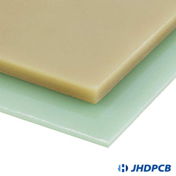
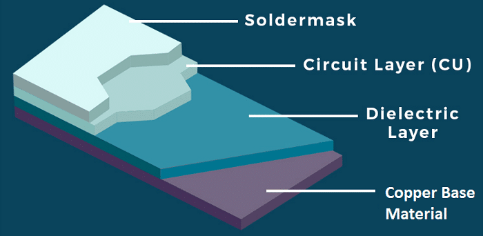
The structure of a copper-based PCB board consists of several key components that contribute to its functionality and performance.

Firstly, the circuit layer of the PCB must have a substantial current-carrying capacity, which necessitates the use of thicker copper foil typically ranging from 35μm to 280μm in thickness. This allows for efficient conduction of electrical currents within the PCB.

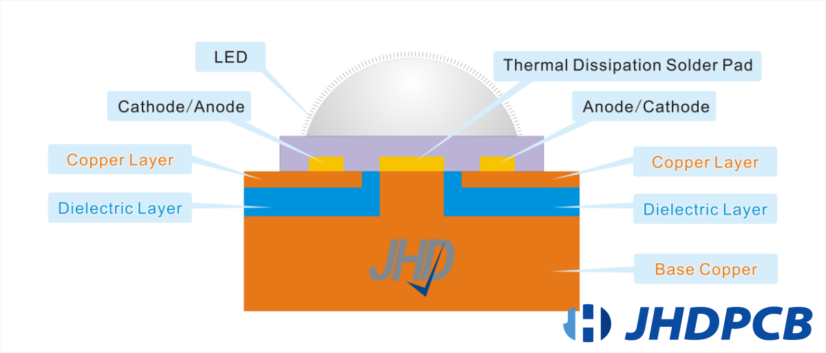
The core technology of the copper-based PCB lies in its thermally conductive insulating layer, which is crucial for managing heat dissipation. This layer is composed of materials such as aluminum oxide and silicon powder, which possess high thermal conductivity properties.

Furthermore, the PCB utilizes a polymer composition filled with epoxy resin, which features a low thermal resistance (0.15) and demonstrates outstanding viscoelasticity, resistance to thermal aging, and durability in the face of mechanical and thermal stress. These characteristics are essential for ensuring the durability and reliability of the PCB.

Furthermore, the metal base of the copper Core PCB serves as a supporting member that requires high thermal conductivity. Usually composed of copper, this metallic substrate is well-suited for traditional machining techniques like drilling, punching, and cutting. The metallic layer also plays a vital function in dissipating heat, providing shielding, covering, or grounding within the structure of the PCB.

In summary, the structure of a copper-based PCB board comprises a circuit layer with thick copper foil, a thermally conductive insulating layer, an epoxy resin-filled polymer composition, and a metal base that collectively contribute to the PCB’s electrical and thermal performance.

What is the feature of Thermoelectric separation?

feature of Thermoelectric separation

Thermoelectric separation offers a range of advanced features that enhance heat dissipation in electronic devices. These features include direct thermal contact, high thermal conductivity, low thermal resistance, electrical insulation, customizable design, improved reliability, and wide-ranging applicability. Let’s explore each of these features in detail:

  1. Direct Thermal Contact:
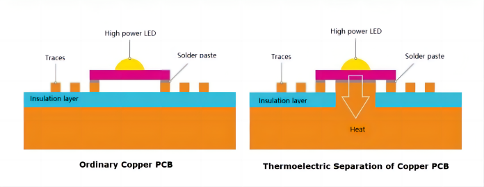
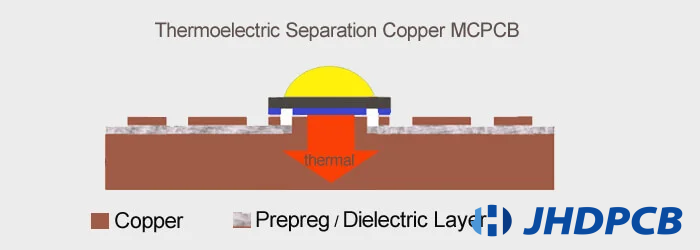
    Thermoelectric separation substrates enable direct contact between the thermal layer and the heat-generating components, such as LED chips or power modules. This direct contact allows for efficient transfer of heat from the components to the thermal layer, minimizing thermal resistance and maximizing heat dissipation.
  2. High Thermal Conductivity:
    The thermal layer of thermoelectric separation substrates is typically made of highly thermally conductive materials, such as copper or aluminum. These materials possess exceptional thermal conductivity characteristics, enabling swift and efficient dissipation of heat from the components.
  3. Low Thermal Resistance:
    One of the key advantages of thermoelectric separation is the aim to achieve low or even zero thermal resistance between the thermal layer and the heat dissipation part. This minimizes the impedance to heat flow, allowing for efficient dissipation and preventing heat buildup within the device.
  4. Electrical Insulation:
    The circuit layer of the thermoelectric separation substrate is made of an insulating material, such as ceramic or polyimide. This insulation layer ensures electrical isolation between the circuit components and the thermal layer, preventing any electrical short circuits or interference.
  5. Tailorable Design:
    Thermoelectric isolation substrates can be customized to fulfill precise design specifications. The dimensions, thickness, and layout of the layers can be adjusted to accommodate various electronic devices and optimize heat dissipation performance.
  6. Improved Reliability:
    By effectively dissipating heat, thermoelectric separation contributes to improved reliability and longevity of electronic devices. It helps to prevent temperature-related failures, reduces the risk of thermal stress on components, and enhances overall system performance.
  7. Wide Range of Applications:
    Thermoelectric technology is applicable to various electronic devices that require efficient thermoelectric heat dissipation, including high-power LEDs, power modules, automotive electronics, computer systems, and more. It provides a versatile solution for managing heat in diverse applications.

What are the advantages and disadvantages of Thermoelectric separation?

difference between Thermoelectric and ordinary

Advantages of thermoelectric separation:
  1. No moving parts: Thermoelectric separation does not require any moving parts, making it a reliable and low-maintenance technology.
  2. Silent operation: Thermoelectric isolation systems function silently, rendering them suitable for application in noise-sensitive environments.
  3. Compact size: Thermoelectric separation systems are typically smaller and more compact than traditional separation methods, making them suitable for use in limited space.
  4. Environmentally friendly: Thermoelectric separation does not use any harmful chemicals or produce any emissions, making it an environmentally friendly option.
  5. Versatility: Thermoelectric separation can be used for a wide range of applications, including cooling, heating, power generation, and temperature control, making it a versatile technology.
  6. Reliability: With no moving parts, thermoelectric separation systems are less prone to mechanical failure, resulting in higher reliability and longer lifespans.
  7. Precise temperature control: Thermoelectric separation allows for precise and accurate temperature control, making it suitable for applications where temperature stability is crucial, such as in medical devices or laboratory equipment.
  8. Solid-state operation: Thermoelectric separation operates using solid-state technology, which means it is not affected by orientation, making it suitable for use in various positions and environments.
  9. Low vibration: Since thermoelectric separation systems do not have moving parts, they produce minimal vibration, which can be advantageous in applications where vibration can affect the performance of other equipment.
  10. Remote operation: Thermoelectric separation systems can be easily controlled and operated remotely, making them suitable for use in unmanned or hard-to-reach locations.
Disadvantages of thermoelectric separation:
  1. Limited efficiency: Thermoelectric separation systems have relatively low efficiency compared to other separation methods, which can result in higher energy consumption.
  2. Limited temperature range: Thermoelectric separation is most effective within a limited temperature range, which may limit its applicability in certain applications.
  3. Significant expense: Thermoelectric isolation systems can incur high costs for installation and upkeep, making them comparatively less cost-efficient than alternative separation methods.
  4. Limited scalability: Thermoelectric separation may not be as easily scalable as other separation methods, making it less suitable for large-scale industrial applications.

Parameters of Thermoelectric Separation Metal PCB

Parameters of Thermoelectric Separation

Thermoelectric separation Metal PCBs are designed to provide localized cooling or heating in electronic and optoelectronic devices. The parameters of the thermoelectric separation Metal PCB are as follows:

ParameterTypical Range
Operating Temperature-40°C to 150°C
Thermal Conductivity1.0 W/mK to 3.0 W/mK
Electrical Conductivity1.0 S/m to 5.0 S/m
Thickness0.2mm to 3.0mm
Dielectric Strength1.5 kV/mm to 3.0 kV/mm
Surface FinishHASL, ENIG, OSP
Copper Thickness1oz to 3oz
Solder Mask ColorGreen, black, blue, red
Minimum Trace Width/Spacing0.1mm to 0.2mm

The exceptional thermal conductivity of materials within the typical range of 1.0 W/mK to 3.0 W/mK ensures efficient heat dissipation throughout the device, facilitating superior temperature management. Coupled with surface finishes such as HASL, ENIG, or OSP, the PCB is endowed with improved solderability and protection against environmental factors, thereby enhancing its durability and performance reliability.

Boasting a single-layer structure, the PCB design achieves a streamlined profile, perfectly accommodating environments where space is at a premium. With minimum trace width and spacing set between 0.1mm to 0.2mm, the board allows for intricate circuit designs and high-density component placement, essential for sophisticated electronic assemblies.

The material thickness ranging from 0.2mm to 2.0mm provides versatility, catering to various application needs from flexibility to structural rigidity. This characteristic, in harmony with an operating temperature spectrum of -40°C to 150°C, guarantees that the PCB can reliably perform under a wide array of thermal conditions.

Dielectric strength values from 1.5 kV/mm to 3.0 kV/mm indicate the PCB’s capability to withstand high voltage environments without breakdown, ensuring electrical safety and integrity. The copper thickness, available from 1oz to 3oz, supports varied current-carrying requirements, making the PCB adaptable to different power needs.

The PCB’s surface can be finished with a selection of solder mask colors, including green, black, blue, and red, which not only provides visual customization but also aids in preventing solder bridging during assembly processes.

Electrical conductivity, in the range of 1.0 S/m to 5.0 S/m, allows for efficient signal transmission, which is crucial for the reliable operation of electronic circuits. This property is particularly important in applications requiring precise electrical performance, such as in sensitive analog circuits or high-speed digital interfaces.


What's the application of Thermoelectric separation copper PCB?

The thermoelectric separation copper PCB has several applications in various industries. The primary application is in the field of power electronics, where high thermal conductivity and electrical insulation are critical requirements. Some specific applications of thermoelectric separation copper PCBs include:

  1. LED Lighting: Thermoelectric separation copper PCBs are used in high-power LED lighting applications. They provide a reliable, efficient, and cost-effective solution for dissipating heat generated by high-power LEDs and maintaining their operational stability.
  2. Automotive Industry: The automotive industry uses thermoelectric separation copper PCBs in electric vehicles (EVs) and hybrid electric vehicles (HEVs). They are used in power converters and battery management systems to ensure stable and reliable performance under high-temperature conditions.
  3. Power Electronics: Power electronics systems such as inverters, rectifiers, and converters require efficient thermal management solutions to maintain their optimal operating temperatures. Copper PCBs with thermoelectric isolation provide exceptional thermal conductivity, minimal thermal resistance, and strong electrical insulation properties, making them well-suited for utilization in these specific applications.
  4. Telecommunications: The telecommunications industry uses thermoelectric separation copper base PCBs in power amplifiers, filters, and other high-frequency circuitry. These PCBs provide excellent signal integrity and thermal performance, contributing to the overall reliability and stability of the communication system.

Overall, the thermoelectric separation copper PCB is a versatile solution that finds applications in various industries that require high thermal conductivity and electrical insulation properties.

What are the technical steps for thermoelectric separation technology of Copper core PCB?

technical steps for thermoelectric separation
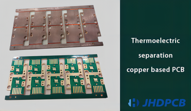
Thermoelectric separation technology for Copper core PCB is a crucial process in the manufacturing of printed circuit boards, especially for applications requiring efficient heat dissipation and thermal management. This advanced technique involves a series of meticulous steps to ensure the proper isolation and protection of the copper core layer while facilitating the integration of circuit patterns and components. Let’s delve into the detailed technical steps involved in the application of thermoelectric separation technology for Copper core PCB:

Step 1: Preparing the Copper Core Layer
The initial stage of the thermal electric separation process involves preparing the copper core layer. This entails ensuring that the copper core layer is immaculate and devoid of any impurities. Additionally, the copper core layer must be trimmed to the appropriate dimensions so that it can be placed between the two layers of prepreg.

Step 2: Applying the Thermoelectric Separation Material
Subsequently, the thermoelectric isolation material is applied onto the surface of the copper layer. Typically, a high-thermal-conductivity insulating material, such as aluminum oxide or silicon nitride, is used. This layer acts as an insulating barrier between the copper layer and the heat sink, preventing the transfer of heat back to the board.

Step 3: Printing the Circuit Pattern
Once the thermoelectric isolation material is applied, the circuit pattern is printed onto the board. The pattern is created using specialized ink containing conductive particles, which form the circuit. The printing process utilizes a photoresist technique, which involves applying a layer of photosensitive material to the board, exposing it to UV light through a mask, and then developing it to create the circuit pattern.

Step 4: Etching the Copper Layer
The next step involves removing any excess copper layer using an etching solution. This process eliminates the copper layer in areas where the circuit is not needed, leaving only the circuit pattern on the board. After etching, the board is cleansed, and any remaining resist is eliminated.

Step 5: Applying Solder Mask and Surface Finish
After the circuit pattern has been etched onto the board, a solder mask is applied to protect the copper traces from oxidation and other types of damage. This mask typically consists of a liquid photoimageable polymer that is coated onto the board and then cured with UV light. Lastly, a surface finish is applied to the exposed copper pads to protect them from corrosion and oxidation.

Step 6: Drilling and Plating
After the surface finish is applied, the board undergoes a drilling process to generate apertures for through-hole components and vias. Subsequently, the holes are coated with a conductive substance to establish electrical connections between the layers of the board.

Step 7: Testing and Quality Control
The final phase in the process involves testing and quality control. The board is examined to ensure that it complies with the specified requirements, including electrical performance and thermal management. Any defects are identified and rectified before the board is dispatched to the customer.

Step 8: Separating the Components
The ultimate step entails separating the components. This is achieved by carefully severing the copper core layer. By utilizing a heat gun to generate heat and a roller press to apply pressure, the copper core layer is heated and softened, enabling its cutting. Once the components are separated, they can be mounted onto the PCB board.

FAQ about thermoelectric separation

Thermoelectric separation can indirectly affect solder joints by managing the heat dissipation on the circuit board. By implementing thermal barriers, it helps to regulate temperature distribution, reducing the risk of thermal stress on solder joints and minimizing the chances of solder joint failure due to excessive heat.

The thermal layer part plays a crucial role in facilitating heat conduction within a circuit board. It is designed to have high thermal conductivity, allowing heat generated by components to spread efficiently across the board. This helps in maintaining a balanced temperature profile and preventing localized hotspots.

Copper core PCBs have excellent thermal conductivity properties, allowing them to efficiently dissipate heat generated by high-power components. The copper core acts as a heat spreader, distributing heat evenly across the board and improving overall thermal management. This helps to prevent overheating and ensures reliable operation of the circuit board.

Thermal relief pads and copper pour areas help reduce thermal resistance in a circuit board design. Thermal relief pads are small copper-free areas around the pins of components, which facilitate soldering while minimizing heat transfer to other areas. Copper pour areas, on the other hand, act as large copper regions that aid in heat dissipation by spreading heat generated by components. Both features contribute to lowering overall thermal resistance and improving thermal management.

A copper substrate, commonly used in metal core PCBs, serves as an excellent conductor of heat. It helps to efficiently transfer heat away from high-power components towards the edges or designated heat sink areas of the circuit board. This ensures effective thermal conductivity and heat dissipation, preventing overheating and maintaining the reliability of the system.

A core PCB design enhances heat dissipation by incorporating a thermally conductive core material, such as copper or aluminum. This core material helps distribute heat evenly throughout the board, allowing for efficient heat transfer to the outer layers where heat sinks or other cooling mechanisms can be employed. Improved heat dissipation reduces the risk of component overheating and enhances overall thermal management.

A heat sink can be incorporated into a circuit board design by adding mounting holes or slots for attaching the heat sink. Additionally, thermal pads or adhesive compounds are used to ensure proper contact and heat transfer between the components generating heat and the heat sink. This allows for effective heat dissipation and temperature regulation.

Traditional copper boards only possess thermal conductivity, whereas thermoelectric separated copper boards can generate electrical energy while conducting heat. Therefore, they have an advantage in applications that require energy recovery or utilization.

It can be used in various automotive applications including climate control systems, engine management systems, battery management systems, and other thermal management systems within the vehicle.

Thermoelectric charge separation clouds refer to hypothetical clouds where temperature differences within the cloud cause the separation of electric charges, resulting in an electrical potential within the cloud.

In conclusion, the utilization of a Thermoelectric separation Copper Substrate represents a significant advancement in the realm of PCB technology. This innovative approach not only enhances the electrical and thermal performance of PCBs but also opens up new possibilities for applications requiring superior heat dissipation and reliable conduction. At JHDPCB, we are committed to pushing the boundaries of PCB technology and providing cutting-edge solutions that meet the evolving needs of our partners and clients in various industries. Please don’t hesitate to reach out to us for any inquiries. Our expert team will offer you technical assistance and solutions, guiding you towards the successful completion of your project.

Get a PCB Quote Now

Open high-quality PCB manufacturing services in JHDPCB

Leave a Comment