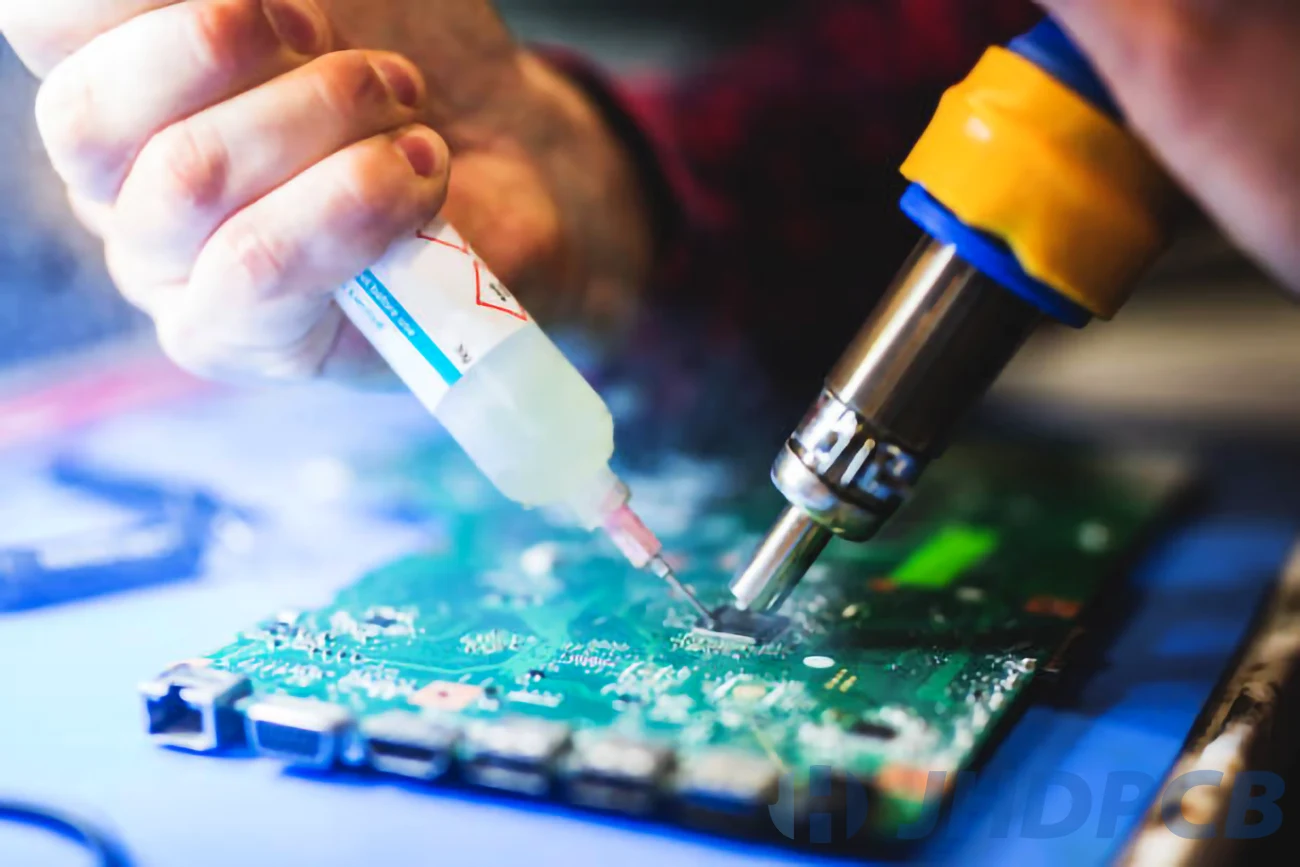
Problem #1 Solder-Bridging
Solder bridging is a common problem encountered in Surface Mount Technology (SMT) assembly, which can result in electrical shorts and circuit malfunctions. There can be various reasons for solder bridging, but the primary cause is often an issue in the solder paste printing process. Sometimes, when the stars don’t align just right, solder bridging can happen.
It’s like a mismatch between the print arrangement or stencil arrangement and the PCB pad configuration. And if there’s too much solder paste or it’s not the right mix of metal and flux, things can get even stickier. Furthermore, the reflow profile can affect bridging, particularly in the pre-heat area, where slow ramp rates, part contact, and extended soak can cause the paste hot slump phenomenon.
Solution:
First things first, we need to make sure we’re using the right ratio of solder paste metal to flux. Then, we gotta nail that reflow profile. Pay close attention to aligning those stencil apertures to the pads, and make sure you’re placing components with just the right amount of pressure and accuracy. Oh, and here’s a nifty trick: try shrinking the stencil aperture dimensions by 10% or using a thinner stencil. That should help cut down on the amount of solder paste getting all over the PCB. Happy soldering!
Problem #2 Insufficient Solder Joints
Insufficient solder joints or electrical opens are common problems encountered in Surface Mount Technology (SMT) assembly, which can result in circuit malfunctions due to the separation of electrically connected points or the interruption of the intended design of the circuit on the PCB.
The solder paste printing stage of the surface mount process is often the primary contributor to this defect, particularly if there is insufficient solder on the joint or if solder paste clogs the apertures of the stencil. The issue of component lead coplanarity, in which the solder volume is sufficient but fails to make proper contact with both the lead and the pad during reflow, can potentially result in electrical opens. Furthermore, it is worth noting that opens can also arise as a direct outcome of the PCB fabrication process itself.
Solution:
In order to effectively address the problem of inadequate solder joints or electrical opens, manufacturers should give careful consideration to rectifying the aspect ratio, which denotes the relationship between the width of the aperture and the thickness of the stencil. The occurrence of solder paste obstruction within the apertures may be attributed to an aspect ratio that is excessively diminutive. Extreme environmental conditions should also be avoided during the manufacturing process to prevent solder paste contamination. Investigating coplanarity is also crucial to solving electrical opens, and PCB fabrication should be checked with the supplier.
Problem #3 Tombstoning
Tombstoning is a common problem encountered in Surface Mount Technology (SMT) assembly, where a chip component partially or completely pulls off the pad into a vertical position with only one end soldered. Tombstoning is a frustrating consequence of the reflow soldering process, where imbalances in forces wreak havoc on our PCB designs. Uneven heating and differing heat sinks, like those found in PCB layers, can create a discrepancy in temperature across the component terminals. This causes one side to reflow before the other, resulting in a rather peculiar sight – one lead standing upright while the other hangs limply.
But the trouble doesn’t stop there. The solder paste, which should hold the component firmly in place during reflow, can sometimes fall short due to exposure to temperature and humidity. Excessive movement during and after the reflow operation, as well as uneven component placement on pads, can also contribute to this frustrating tombstoning phenomenon.
Solution:
In order to effectively tackle the issue of tombstoning, manufacturers must prioritize the incorporation of a component body that covers at least 50% of both pads. This strategic approach will effectively mitigate any potential imbalance in solder forces, thereby ensuring the maintenance of impeccable component placement accuracy. A high preheat temperature can also minimize the differential between the two ends during reflow, and minimizing movement during SMT assembly can prevent component misalignment. Furthermore, by strategically reducing the impact of environmental extremes, such as scorching heat or excessive humidity, and incorporating a well-designed extended soak zone, the equilibrium of wetting force on both pads can be effectively harmonized prior to the paste transitioning into a molten state.
Problem #4 Non-Wetting or De-Wetting
Non-wetting or de-wetting, a notorious hurdle in Surface Mount Technology (SMT) assembly, occurs when the fluid solder fails to establish a close bond with one or more components. It also arises when a surface comes into contact with liquid solder but fails to retain any or only a portion of the solder. The presence of a subpar PCB finish, where the underlying metal is exposed and poses challenges for soldering, often acts as a primary culprit behind this vexing issue. Additionally, soaking time that is too long in the reflow process can exhaust the flux before soldering, and insufficient heat during the reflow process can prevent the flux from reaching the proper activation temperature.
Solution:
To tackle the problem of non-wetting or de-wetting, manufacturers should explore the adoption of superior metal surface finishes that exhibit higher temperature resistance, such as OSP or ENIG. Additionally, optimizing the overall profiling time prior to the reflow stage can prove beneficial in addressing this issue. Furthermore, selecting the proper flux for the given soldering task is crucial.
Problem #5 Solder balling
It is a common problem encountered in Surface Mount Technology (SMT) assembly, where very tiny spherical particles of solder isolate from the main body, forming the joint. Solder balling poses a significant concern for no-clean processes, as it can create deceptive connections between adjacent leads, ultimately causing functional issues within the electrical circuit.
Moisture contamination of the solder paste stands as a primary culprit behind the formation of these solder balls, as the moisture saturates and leaves behind tiny spheres during the reflow process. Additionally, a lack of proper reflow profile, an excessively rapid preheat rate, and the presence of excessive oxides on the solder powder within the solder paste can all contribute to the occurrence of solder balls.
Furthermore, poor alignment during solder paste printing, wherein the paste is mistakenly applied onto the solder mask instead of the intended pad, as well as the inadvertent smearing of solder paste on the underside of the stencil during the printing process, can further exacerbate the issue of solder balling.
Solution:
In order to effectively address the issue of solder balling, it is advisable for manufacturers to explore the utilization of coarser powder sizes. This is because fine powder sizes often contain more oxides, making them more prone to slumping. Additionally, it is imperative to carefully select the appropriate reflow process based on the specific solder paste being used, while also taking measures to prevent any negative interactions between the paste and moisture or humidity.
Furthermore, it is crucial to thoroughly inspect and regulate the minimum print pressure applied, as well as consistently verify print alignment prior to proceeding with the reflow process. Lastly, ensuring the bottom of the stencil is regularly and thoroughly cleaned is of utmost importance.
Problem #6 Solder Beading
Solder beading is a common problem encountered in Surface Mount Technology (SMT) assembly, where bigger solder balls form close to discrete components with very low distances from each other.
This anomaly bears resemblance to solder balling, yet it exhibits a discrete nature as these solder beads stubbornly adhere to individual components rather than multi-leaded devices. The primary culprit behind the formation of these solder beads is typically an excessive deposition of solder paste.
Additionally, during the preheat stage, the outgassing of flux can overpower the force of paste coalescence, while excessive pressure during component placement can push the deposited solder paste onto the solder mask, hindering its ability to seamlessly fuse back into the joint.
Solution:
To tackle the pesky problem of solder beading, manufacturers are advised to contemplate the art of stencil thickness reduction or, alternatively, the reduction of aperture dimensions. Specifically, focusing on the side where the solder bead chooses to make its unwelcome appearance. A mere reduction of 10% in either aspect should work wonders in banishing this issue from existence.
Problem #7 Cold Solder Joint
The phenomenon known as cold solder joint, or grainy joint, is a frequent issue encountered in the realm of Surface Mount Technology (SMT) assembly. This problem arises when certain solder connections exhibit poor wetting, resulting in a greyish and porous appearance after the soldering process. Instead of the expected bright and shiny alloy surfaces, these connections appear dark, non-reflective, and rough.
Insufficient heat absorption by the solder stands as one of the primary causes behind cold solder joint. In such cases, the available heat for reflowing the solder falls short of what is required. Moreover, during SMT soldering, the flux may prove incapable of fulfilling its duty due to inadequate cleaning of the components and/or the PCB pads prior to soldering. Furthermore, an excessive number of impurities in the solder solution can also contribute to the development of this defect.

Solution:
To tackle the problem of cold solder joints or those grainy little devils, manufacturers gotta crank up the reflow temperature to the max. No half-baked solutions here! And hey, no jiggling or jostling the assembly during or right after reflow. Oh, and don’t forget to give those alloys a good ol’ analysis to weed out any sneaky contaminants. Can’t have those messing up the party!
Problem #8 Insufficient Fills and Insufficient Solder
Having too little solder in your Surface Mount Technology (SMT) assembly is a total bummer. It happens when the amount of solder paste put on the printer station is way less than what the stencil opening design calls for. And to make matters worse, sometimes there’s not enough solder left after reflow to form a nice little fillet on the component leads.
You know what causes this headache? A blocked-up stencil aperture. When the paste dries up and clogs the stencil, it’s like a traffic jam on the road to a perfect assembly. So, during the printing process, you gotta apply enough pressure on that squeegee blade to wipe the stencil clean. But be careful not to go overboard and scoop up too much paste, especially on those big pads. That can lead to a big ol’ defect.
Oh, and here’s another thing to watch out for if the paste is too runny or doesn’t have enough metal content, it won’t roll into the aperture properly because the squeegee is moving too fast.
Solution:
To solve the issue of insufficient fills and insufficient solder, manufacturers should consider segmenting the large opening into smaller apertures and checking for too much squeegee pressure. Make sure to clean that stencil regularly and double-check the paste for any signs of expiration or dryness. Additionally, ensuring sufficient board support and controlling excessive squeegee speed is crucial.
Problem #9 Signal Integrity
One of the most critical considerations for SMT assembly is signal integrity. Improper placement of SMT components in relation to their circuits can cause signal integrity issues, leading to reduced performance or even complete failure of the board.
Solution:
To avoid any mishaps, PCB layout designers need to play a game of connect-the-dots with their parts, making sure they follow the signal paths shown in the schematics. It’s like a high-stakes puzzle where precision is key! Moreover, they should isolate digital and analog parts in their design partitions to prevent interference. It is also essential to place components in such a way that clear signal return paths are available on the reference plane.
Problem #10 Power Integrity
Another crucial consideration for SMT assembly is power integrity.
Solution:
If you want to make sure that power is delivered smoothly, you gotta put those bypass capacitors right next to their supply pins. This way, you’ll lower the chances of any annoying noise messing up your power delivery network. Oh, and don’t forget to keep those power supply components nice and cozy on the same board layer. That way, you’ll have shorter connecting traces and less inductance in the line.
Problem #11 PCBA Rework
Rework is a crucial part of the PCB manufacturing process, whether it involves inspection, repair, or replacement of parts during assembly. However, SMT parts hidden behind larger parts can make rework and inspection challenging. Repair and testing tools may not fit where they are needed, leading to collateral damage to nearby parts.
Solution:
To avoid this, designers should consider the accessibility of SMT components during the design phase.
Problem #12 Testability
If you put those SMT components too close to the test points, it’s gonna mess things up. The test probes won’t be able to make contact, and that’s not good for quality control testing. And if you go ahead and place an SMT component right over the test points, well, you can forget about testing them altogether.
Solution:
So, here’s what we gotta do. Designers need to be smart about where they put those SMT components, so that we can easily access those test points. Problem solved!
Problem #13 Shadowing
Shadowing is a common problem encountered when small surface mount components on boards are wave soldered. If a smaller part follows a larger component into the wave, it may not receive enough solder, resulting in insufficient electrical connectivity.
Solution:
To dodge this pesky problem, designers should play a clever game of hide-and-seek with their components. Simply put, they should make sure the little guys take the spotlight in front of their big buddies. By doing so, they’ll not only prevent any sneaky shadows, but also guarantee a flawless soldering experience. So, let the small fry shine and wave goodbye to any soldering mishaps!