Printed Circuit Board Terminology You Should Know – PCB Glossary
What are the Terminology of PCB Design?
Many individuals utilize online resources to create printed circuit board (PCB) designs; however, at times it can be challenging to comprehend the terminology associated with PCB design. In this article, I aim to clarify common terminology in pcb design. PCB refers to a board utilized for printed circuits. There are various kinds of materials used in PCB manufacturing that are readily available in markets such as FR-1, FR-2, CEM-3, and CEM-1, where FR stands for Flame Retardant and CEM stands for Composite Epoxy Material.
Below are some commonly utilized pcb design terminology:
1. Layers
All drawings in PCB design are performed on a specific layer, each of which possesses unique physical characteristics. For instance, the top layer is utilized to create a layout for the components, whereas the bottom or inner layers enable interconnections between components. Furthermore, several additional layers exist to serve various purposes in PCB design.
2. Footprint
A footprint in PCB design is comprised of a set of pads and outlines that represent a single component. Most PCB design software comes equipped with a pre-existing library that includes footprints for various components; however, the number of available footprints is frequently limited. In modern times, technology continues to evolve, resulting in smaller component sizes. Consequently, it may be necessary to create a custom footprint for an individual component.
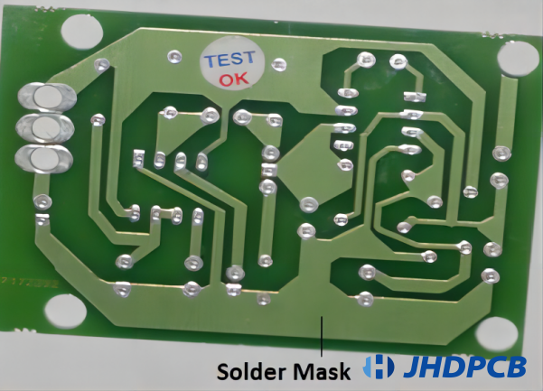
3. Solder mask
Most of you have observed the presence of a green, red, blue, or glossy coating on PCBs, which is referred to as a solder mask. Masking on PCBs is applied to prevent accidental deposition of solder on the board and to facilitate the process of component soldering. Additionally, it prevents short circuits between adjacent tracks. Novices in PCB design may use excessive solder when soldering, leading to short circuits. However, having a solder mask makes it easier to remove excess solder without melting anything, given that it is a non-conductive layer on the PCB.
4. Silkscreen
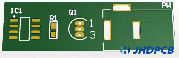
In PCB design, silkscreening is performed to display component names or values, making it easier for the user to identify individual components while soldering. This practice is highly recommended when designing PCBs and can be executed on both sides of the board, either on the component side or copper side. Silkscreening can also be utilized to indicate the company or manufacturer name. Like a solder mask, silkscreening is a non-conductive layer of the PCB.
5. Jumper
A jumper wire is an electrical conductor used to establish a connection between two specific points on a printed circuit board. Occasionally, while designing PCBs, it may become necessary to use jumper wires if traces overlap one another when attempting to establish connections.
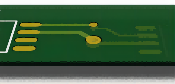
6. Pads
On printed circuit boards, pads are utilized to create connections between components and tracks via the use of solder. These small patches of copper are commonly employed to establish robust mechanical joints by soldering component leads onto the board. Because surface mount components and through-hole components vary in shape and size, different types of pads are used for each.
7. Copper traces
On printed circuit boards, copper traces are utilized to connect pads and vias. These lines are commonly green, blue, or red in color and provide electrical conductivity between pads, vias, or between two pads and/or vias. The width of a trace varies depending on the magnitude of current that will flow through it.
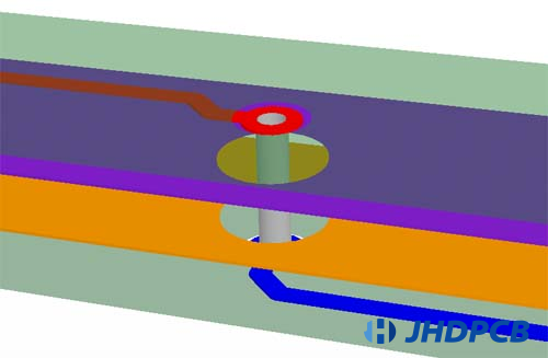
8. Via
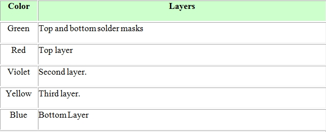
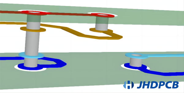
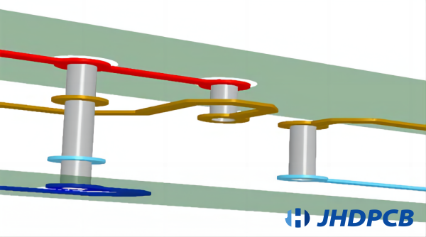
When designing a multilayer printed circuit board, it may be necessary to establish connections between the top and bottom layers, which can be accomplished through the use of vias. A via is a conductive channel that passes through the board, allowing current to flow between layers. This can be easily observed in the diagram provided, where yellow-colored pads represent the bottom layer, green-colored pads represent the top layer, and the circular yellow components depicted are vias.
In a multilayer printed circuit board, it is common practice to utilize specific colors to indicate each layer. These colors serve as visual indicators of the various layers present in the PCB.
The PCB depicted in the diagram features a top layer track that extends through the board using a through-hole via, subsequently transitioning into a bottom layer track.
9. Blind via
In the design of integrated circuits – particularly those featuring more complex circuits and utilizing multiple power planes (such as Gnd and Vcc) – it is often beneficial to make use of vias. These vias are generally situated between the top and second layers, rather than at the bottom layer, and are referred to as “blind” vias. Blind vias simplify the process of establishing direct connections to power planes beneath chips, as opposed to routing lengthy tracks. They are used in cases where connections need to be made between external and internal layers whilst minimizing via height.
To distinguish between through-hole and blind vias, one can hold a PCB up to a light source and observe whether or not light passes through the via. If light is visible, then the via is through-hole in nature, whereas a lack of visible light indicates a blind via. This technique proves to be especially useful in instances where limited space is available for component placement and routing. Should through-hole vias be utilized instead of blind vias, additional via space on both sides would be necessary.
In the figure provided, a single blind via connects the top and inner layers (indicated in red and yellow), while another connects the inner and bottom layers (indicated in blue and light blue). The version of the figure featuring all three colors represents a through-hole via connecting the top and bottom layers.
10.Buried Vias
- Buried vias are akin to blind vias in that both serve to establish connections between different layers of a printed circuit board. However, while blind vias connect either the top or bottom layer with an internal layer, buried vias exclusively connect internal layers.
As can be seen in the figure provided, the colors yellow and light blue are indicative of buried vias. One can compare all three types of vias as follows:
The first type, featuring red, yellow, light blue, and blue colors, represents a through-hole via.
The second type, composed of red and yellow colors, corresponds to a blind via.
And finally, the third type, featuring yellow and light blue colors, represents a buried via.
The primary drawback of incorporating buried vias in a printed circuit board is that it drives up the overall cost compared to using through-hole vias. Nevertheless, buried vias are advantageous as they occupy less space. As such, the selection of via type hinges on specific project requirements, with consideration given to factors such as size and cost.
11. Gerber
When it comes to the fabrication of printed circuit boards, users will typically submit a Gerber file to their chosen manufacturer. The reason for this lies in the fact that numerous PCB design software packages are currently available, meaning that there is no guarantee that a given software will be supported by all vendors. Therefore, in the event that your manufacturer lacks access to the same software package that you used to create your PCB design – let’s say, for instance, that you created your design using Eagle software – sharing a Gerber file will prove invaluable. A Gerber file provides the manufacturer with comprehensive information about your project and should not be altered in any way. In essence, a Gerber file serves as a blueprint for the PCB’s fabrication, specifying key details such as drill bit size, hole placement, track connections, and component names.
12. BOM
BOM is an acronym that stands for “bill of materials.” This document provides a compre
hensive list of all components featured on a given printed circuit board, enabling users to tally up approximate costs and streamline the ordering process. Moreover, a BOM affords users peace of mind by allowing them to double-check for any inadvertently omitted components.
13.Schematic
In electronics design, a schematic – also known as a circuit diagram – is a graphical representation of an electronic circuit using standardized symbols and notations which make up the circuit board shorthand, to depict the electrical connections between various circuit components.Some examples of PCB shorthand include “R” for resistor, “C” for capacitor, “L” for inductor, “D” for diode, “Q” for transistor, “+” for power supply voltage, “-” for ground, and many others. Schematics serve as a blueprint for the final PCB design, providing valuable insights into the functional and technical details of the circuit. Typically, schematics are created in specialized software tools such as Eagle, Altium Designer or KiCad.
Common PCB Design Software:
- Altium Designer: A comprehensive electronics design software that allows designers to create schematics, perform PCB layout, and generate manufacturing output files. It features advanced routing tools, 3D visualization, and simulation capabilities.
- Eagle PCB: A popular PCB design tool for small to mid-size businesses and individuals. It provides an intuitive interface for schematic capture and PCB layout, as well as an extensive library of pre-built components.
- KiCAD:A free open-source software suite for electronic design automation (EDA). It includes schematic capture, PCB layout, and 3D visualization tools and has a large and active community of users who provide support and resources.
- OrCAD: A PCB design and analysis tool suite that includes schematic capture, PCB layout, and simulation tools. It is widely used in the industry and has been around for many years.
- PADS PCB: A PCB design tool by Mentor Graphics that includes schematic capture, PCB layout, and routing tools. It also provides advanced simulation and analysis capabilities.
- Proteus PCB: An all-in-one electronics design software that includes schematic capture, PCB layout, simulation, and debugging tools. It is particularly useful for designing mixed analog and digital circuits.
- CircuitMaker: A free PCB design tool by Altium that provides an easy-to-use interface for schematic capture and PCB layout. It includes a vast library of pre-built components and provides collaboration features for teams.
These software tools provide designers with the ability to create schematics, place components, route traces, and generate manufacturing data for PCB fabrication.
It’s important for designers to communicate effectively using common terminology to avoid misunderstandings and errors during the design process and to select the most appropriate software tool for the project based on their specific needs and requirements.
Glossary of commonly used PCB fabrication and process terms.
Understanding PCB fabrication terminology is crucial for producing high-quality circuit boards that meet industry standards.The following are PCB manufacturing terms:
Additive Process – The process of adding conductive material to a base material, whether it be coated or uncoated, is known as deposition or addition.
Ambient – This refers to the conditions in which a system or component is exposed to contact with its external surroundings.
Annular Ring –This refers to the conductive material encircling a hole in its entirety.
Anti-Tarnish – A chemical treatment process performed after a procedure, used to prevent or impede the oxidation of copper circuits.
Array – This refers to an assemblage of components or circuits which have been organized in a grid pattern on a substrate.
Artwork – This refers to a precisely proportioned layout of electronic information utilized in the creation of an artwork or production master.
Artwork Master – This refers to a photographic representation of the printed circuit board pattern on film, which is employed in the production of the circuit board, usually at a 1:1 scale.
Aspect Ratio –This refers to the aspect ratio of a printed circuit board, which represents the relationship between its thickness and the size of the smallest hole it contains.
B-Stage –This refers to a stage in the chemical reaction of a thermosetting resin, whereupon heating the material undergoes partial softening and swelling, without complete melting or dissolving, when exposed to specific liquids.
Backup Material – This refers to a rigid and flat substance utilized as support when drilling through laminate material, with the goal of minimizing any jagged edges or unevenness.
Backplane – This refers to an extensively sized printed circuit board designed to accommodate a multitude of pins for the purpose of wire wrapping.
Barrel – This refers to the tube created by coating the interior of a drilled hole through the process of plating.
Bare Board – This refers to a printed circuit board that has not yet been fully assembled, including the absence of any electronic components.
Base Material – This refers to the non-conductive substance utilized for shaping the conductive design on a circuit board, which can have both rigid and flexible properties. It may also take the form of either a dielectric or an insulated sheet of metal.
Base Material Thickness – This refers to the thickness of the substrate material, not including any metal foil or surface coatings deposited upon it.
Bed of Nails –This refers to a testing device comprised of a frame and a receptacle containing an array of spring-loaded pins that establish electrical connectivity with a flat test object.
Blind Via – This describes a via that passes through only one surface of a printed circuit board and does not extend between the top and bottom layers.
Blister – This refers to a specific area of swelling and/or separation that occurs between any of the layers of a laminated substrate material, or between the substrate material and conductive foil, and is a type of delamination.
Blanking Die – This refers to the process of using a die punch to “blank out” or cut the completed circuit board, which is primarily utilized for single-sided panels.
Blow Holes – This describes the presence of blow holes that result from a burst of gas emanating from the solder fillet on a circuit board during the soldering process.
Board Thickness – This refers to the total thickness of the substrate material and all conductive materials deposited on it.
Book – This refers to a designated quantity of prepreg layers that are combined with inner-layer cores prior to being cured in a lamination press.
Bond Strength – This defines the interlayer peel strength of a circuit board, which denotes the force required to delaminate two adjacent layers of the board in a direction perpendicular to the board surface per unit area.
Bow – This refers to the degree of non-flatness of a circuit board, which is characterized by a somewhat cylindrical or spherical curvature that results in the four corners of the rectangular product lying on a common plane.
Border Area –The excess base material surrounding the edges of the final product being produced is referred to as the panel margin or panel border.
Buried Via – A hole that is drilled through the internal layers of a multilayer circuit board but does not penetrate the outermost layers.
Burr – A raised edge or bump that encircles a hole on the outer copper surface resulting from the drilling process.
C-Stage – A dielectric material that has been completely cured to its final state.
C-Stage Resin – A cured resin that has achieved its final level of curing.
CAM– (Computer Aided Manufacturing) – The utilization of computer systems, software programs, and procedures that involve human operators in decision-making during different stages of the manufacturing process while computers provide functions to manipulate data.
CAM Files – The data files utilized directly in the production of printed circuit boards. The file formats include: (1) Gerber data, which governs a photoplotter. (2) NC Drill data, which governs an NC Drill machine. (3) Digital drawings in formats such as Gerber, HPGL, or any other compatible format used for the manufacturing of printed circuit boards.Physical copies of prints may also be available. Computer-aided manufacturing (CAM) files represent the final outcome of PCB design. These files are provided to the PCB manufacturer, who further refines and manipulates the CAM data in their processes, such as in step-and-repeat panelization.
Card – A synonym for a printed circuit board is a circuit card.
Capacitance – The characteristic of a system comprising dielectrics and conductors that permits the retention of electrical charge when voltage is present between the conductors.
Catalyst – A substance employed to start or accelerate the reaction between a curing agent and a resin.
Caul Plates – Stable, flat, polished steel plates that are inflexible in nature and are used during the lamination or pressing of multilayer printed circuit boards.
Center to Center Spacing – The rough estimate of the distance between the central points of neighboring elements on a single layer of a printed circuit board, including surface mounts and gold fingers, is known as the pitch.
Circuit – An assembly of electrical components and devices that have been linked together to accomplish a specific electrical purpose.
Clad – A copper structure present on a printed circuit board. When designating particular text elements as “in clad,” it indicates that the text must be made of copper rather than silkscreen.
Overlay – A state in which a thin sheet or layer of metal foil has been attached to one or both sides of a substrate material.
Clearance Hole – A hole within the conductive design that is larger in size and aligned with a hole present in the base material of a printed circuit board.
Component – One of the fundamental components utilized in constructing electronic devices, such as resistors, capacitors, connectors, DIPs, etc.
Component Hole – A drilling on a printed circuit board utilized for securing and/or electrically linking component terminals, such as wires and pins.
Component Side –The layer of the printed circuit board where most of the components are placed, also referred to as the component layer or the front layer.
Conductive Pattern – The pattern or configuration of the conductive material on a substrate material, which includes conductors, pads, holes, heat dissipation structures, and passive components when they are integral to the fabrication process of the printed circuit board.
Conductor Spacing –The visible measurement between the neighboring edges (excluding center-to-center spacing) of individual patterns within a conductor layer.
Continuity – A continuous route for the passage of electric current within a circuit.
Conformal Coating – A conformal coating is a layer of protective and insulating material that conforms to the shape of the assembled printed circuit board and is applied as a final step in the manufacturing process.
Connection – A single branch of a net.
Connector – A connector or socket that can be effortlessly connected to or disconnected from its counterpart. Multi-contact connectors unite two or more conductors with others to form a single mechanical assembly.
Controlled Impedance – The process of aligning substrate material characteristics with trace dimensions and positions to generate a precise electrical impedance for a signal as it travels along a trace.
Conversion Coating – The application of an anti-oxidation treatment to unprocessed foil obtained from a supplier.
Core Thickness – The depth of the laminate substrate without any copper layers.
Crosshatching – The division of a sizable conductive area through the utilization of a void pattern within the conductive material.
CTE – (Coefficient of Thermal Expansion) – The assessment of how much a material alters in any axis for each degree of alteration in temperature.
Curing – The process of utilizing temperature and pressure to affix laminate materials together.
Database – A group of correlated data elements kept together in a non-repetitive manner to support one or multiple applications.
Date Code – The process of labeling merchandise to indicate the date of its production, following the ACI standard of WWYY (week week year year).
Datum – The precise hypothetical spot, axis, or plane that acts as the reference point for determining the position of geometric attributes of features of a component.
Delamination – The division of layers within a substrate material, between a substrate material and a conducting foil, or any other flat division present in a printed circuit board.
DES – The procedure of developing, etching, and stripping employed in the etching stage of manufacturing inner layers.
Design Rule Checking –The utilization of a computer-assisted software to conduct continuity confirmation of all conductive pathways routing in compliance with relevant design principles.
Desmear – The elimination of melted resin caused by friction and debris resulting from the drilling process, from the wall of a drilled hole.
Dewetting: This refers to a situation where a surface has been covered by molten solder and subsequently withdrawn, resulting in unevenly shaped bumps separated by thin areas of solder. The underlying material remains concealed.
Dielectric – An element possessing a significant impediment to the passage of electricity and the ability to become polarized by an electric field.
Dimensional Stability – A metric of the alteration in size of a substance resulting from various factors such as variations in temperature, humidity, chemical treatment, and stress exposure.
Dimensioned Hole – A perforation in a printed circuit board whose position is established by physical measurements or coordinate values that may not align perfectly with the designated grid.
Direct Plate – The process of depositing conductive coatings onto drilled holes to ensure electrical connectivity for electrolytic plating.
DOE – Experimental design… a structured approach to developing an interactive test plan.
Dog Bone – A deficiency in plating observed in drilled holes where the copper electroplating is thinner at the center and thicker at the edges.
Double-Sided Board – A double-sided printed circuit board is a type of circuit board that has conductive traces and features on both top and bottom surfaces.
“Double-Track” is a colloquial term used to describe a narrow design involving two traces between dual inline package (DIP) pins.
Double Treat – A coating made of brass applied to copper foil in place of oxide.
Dry-Film Resists – A type of coating material formulated for the fabrication of printed circuit boards and chemically-machined components that effectively withstands a range of electroplating and etching procedures.
Dry Film Solder Mask – A photo-imaged solder mask film that is applied to a circuit board, capable of accommodating the higher precision demanded by surface mount technology and fine line designs.
Electrod Eposition – The process of depositing a conductive substance from a solution used in plating through the use of electrical charge or current.
Electro Less Deposition –Auto-catalytic plating, also known as electroless plating, is a process of depositing conductive material from a plating solution without requiring an external electrical current or charge.
Electroplating – Electroplating involves the process of depositing a metal coating onto a conductive item. Electroplating is a process in which an object is submerged into an electrolytic solution and connected to one terminal of a direct current (DC) voltage source, while the metal to be deposited is also immersed in the same solution and connected to the other terminal.
Entry Material – A thin metal foil, typically made of aluminum, that is affixed to the top surface of a drill stack to reduce burrs created during drilling and provide cooling for the drill tip.
Etchback – Selective chemical etching involves the precise removal of non-metallic substances from hole sidewalls to expose more internal conductor surfaces and eliminate resin smear, all at a specified depth.
Etching – Chemical or chemical and electrolytic means are employed to eliminate unwanted areas of conductive or resistive matter in a process known as etching.
Fab – Fabrication.
Fabrication Drawing – A detailed illustration that assists in the production of a printed circuit board, known as a “fab drawing,” displays the precise positions of all holes to be drilled, including their sizes and allowable deviations, board dimensions, and instructions regarding materials and techniques. The illustration establishes a reference point for at least one hole location relative to the board edge, allowing proper alignment of the NC Drill file.
Fiducial Mark – A feature or set of features on a printed circuit board that are produced concurrently with the conductive pattern, and which serve as a consistent and measurable point of reference for attaching components in relation to one or more land patterns.
Fine Pitch – This is in reference to chip packages featuring lead pitches under .050, with the maximum pitch for such parts being around .031 and some having lead pitches as tiny as .020.
Finger –A card-edge connector’s gold-plated contact that is named for its distinctive shape.
First Article – A prototype or set of prototypes produced before mass production to confirm the manufacturing process’s ability to produce a product that meets defined specifications.
Flux – A chemical agent utilized during solder reflow or component attachment for activation purposes.
FPPY – The initial panel yield, which is the number of fully functional “panels” resulting from subtracting the count of faulty panels.
FR-1 – FR-1 is a paper-based material that employs a phenolic resin binder and exhibits a glass transition temperature (TG) of roughly 130°C.
FR-2 – A paper-based material that has a phenolic resin binder, which is akin to FR-1 but with a glass transition temperature (TG) of approximately 105°C.
FR-3 – A paper product resembling FR-2 but incorporating an epoxy resin binder instead of phenolic resin, predominantly utilized in Europe.
FR-4 – FR-4 is the most widely used dielectric material in PCB manufacturing, with a UL rating for a glass and epoxy composite laminate that satisfies the prescribed flammability standard.FR-4 is one of the most commonly used substrate materials for printed circuit boards, made from woven fiberglass cloth and epoxy resin, with excellent mechanical strength and good heat resistance.
G10 – G10 is a laminate material manufactured by subjecting woven epoxy-glass cloth to impregnation with epoxy resin through the application of heat and pressure. Unlike FR-4, G10 does not possess flame-retardant characteristics. It finds application in making thin circuits, for instance, those utilized in watches.
Golden Board – “Known Good Board” (KGB) can be described as a term used to refer to a circuit board that has been confirmed to be fully functional and meets all required specifications.
Ground – A standard grounding location for electrical circuits, used for the purpose of returning signals, providing shielding, or dissipating heat.
Ground Plane – A layer of conductive material, or a section thereof, utilized as a shared reference for returning electrical signals, providing shielding, or dissipating heat in an electrical circuit.
Haloing –Cracking or separation within or beneath the base material, with an observable light-toned region encircling any holes.
Hard Board – A rigid printed circuit board (PCB) is a type of circuit board that has a inflexible substrate material, such as FR4 fiberglass, which provides structural support and stability to the board.
HASL – (Hot Air Solder Leveling) – A process of covering uncovered copper with molten solder by immersing a panel into a solder bath and subsequently moving the panel quickly past streams of heated air.
HDI – (High Density Interconnect) – Multi-layer printed circuit boards (PCBs) with very fine geometries, comprising of conductive microvia interconnections, and often containing buried and/or blind vias. These PCBs are fabricated using sequential lamination techniques.
Hole Breakout – A situation where a land does not fully encircle a hole.
Hole Density – The term “hole density” refers to the number of drilled holes per unit area on a printed circuit board (PCB). It is often used as a measure of the board’s complexity and can impact manufacturing costs.
Imaging – The technique of transmitting electronic data to a photo-plotter device, which utilizes light to imprint a negative image of circuit patterns onto a panel or film substrate.
Immersion Plating – A process of chemically depositing a thin layer of metal onto certain base metals by partially replacing the base metal.
Impedance –Impedance can be defined as the total resistance to the flow of electrical current in a circuit, which is determined by the combination of resistance, capacitance, and inductance of the network. It represents the overall effect of these three elements on the current flow in the circuit.
Inclusions –Foreign materials, which can be composed of metals or non-metals, are substances that may become trapped in an insulating material, conductive layer, plating, base material, or soldered joint. These materials can negatively impact the performance and reliability of electronic components and should be avoided during manufacturing processes.
Inkjetting – The process of applying precise ink dots onto a printed circuit board (PCB). Inkjet technology melts a solid ink pellet with heat, converting it into a liquid form. The liquid ink is then dispensed through a nozzle onto the surface of the PCB and rapidly solidifies.
Inner-Layers – The inner layers of insulating material and metallic foil contained within a multilayer printed circuit board.
Insulation Resistance –Electrical resistivity is a term used to describe the specific resistance of an insulating material. It is measured under specific conditions between any combination of contacts, conductors, or grounding devices. This property of a material describes its ability to resist the flow of electric current and is often used as a measure of the material’s quality and suitability for use in different applications.
KGB– (Known Good Board) – A circuit board or assembly that has been confirmed to be defect-free, often referred to as a reference board or a golden sample.
Laminate – A manufactured item created by firmly joining multiple layers of materials together.
Laminate Thickness – The initial measurement of the thickness of a metal-coated substrate, whether it is single or double-sided, before undergoing any subsequent manufacturing steps.
Laminate Void – A void is the absence of epoxy resin in a cross-sectional area where it is expected to be present.
Land – The section of a printed circuit’s conductive pattern that is specifically allocated for the purpose of mounting or attaching components; this area is commonly referred to as a pad.
Laser Photo-Plotter –A type of plotter that employs a laser to emulate the functionality of a vector photo-plotter, utilizing specialized software to generate a raster image of individual objects contained within a CAD database. The resulting image is produced through the plotting of a sequence of dotted lines at an incredibly high resolution. When compared to a vector plotter, a laser photo-plotter offers enhanced accuracy and consistency. This is due to the laser technology which is capable of achieving higher levels of precision when creating images on a photo-sensitive material. As a result, laser photo-plotters are often preferred for high precision applications in the electronics industry.
Lead – A connector point located on a component.
Legend – A specific style of characters or symbols utilized on a printed circuit board, including but not limited to part numbers, serial numbers, component positions, and patterns.
Liquid Resist –The fluid state of photoresist material employed in the manufacturing of circuits.
LPI –(Liquid Photo-Imageable Solder Mask) –A specialized ink that is utilized to control the deposition of materials using photographic imaging techniques. This type of ink is commonly used in a variety of industries, including electronics manufacturing, to ensure precise and accurate application of materials to surfaces.This method of mask application is the most precise and yields a thinner mask compared to dry film solder masks, making it ideal for densely packed SMT. The ink may be applied through spray, curtain coat, or squeegee methods..
Mask – A substance utilized to facilitate the targeted process of etching, plating, or solder application on a PCB. This compound is commonly referred to as either solder mask, resist, or etch resist.
Measling – Small, distinct white markings or crosses visible beneath the surface of the base laminate that indicate a discontinuity in the fibers within the woven glass cloth at points where they intersect.
Metal Foil – The layer of conductive material on a printed circuit board that serves as the foundation for creating circuits.This metallic thin sheet, commonly made of copper, is provided in either roll or sheet form. It is a widely used material in various industries, and its versatility makes it a popular choice for a wide range of applications.
Micro-Sectioning – The process of preparing a sample of a material or multiple materials for metallographic analysis, typically involving the creation of a cross-sectional cut that is then encapsulated, polished, etched, and stained.
Microvia –Typically referred to as a conductive micro-hole with a diameter of 0.005 inches or less used to interconnect multiple layers of a PCB. The term may also encompass various small connection holes created by laser drilling, regardless of their specific geometries.
Mil – A unit of measurement equivalent to 0.001 inches, often employed to specify material thicknesses below 0.100 inches. This term is commonly known as a mil, or one-thousandth of an inch.
Mil Spec – A set of requirements established by the armed forces, typically referred to as military specifications or MIL-SPECs.
Millionths – A unit of measurement utilized to describe material thickness, equivalent to 100 millionths of an inch or 0.0001 inches. This term is commonly employed as a reference for specifying extremely thin materials. It is often referred to as a ten-thousandth of an inch.
Mother Board – A PCB utilized for connecting grids of pluggable electronic components.
Mounting Hole – An orifice utilized for providing mechanical reinforcement to a printed circuit board or for mechanically affixing components onto a printed circuit board.
Multi-Layer Board – A multilayer PCB (Printed Circuit Board) is a type of circuit board that comprises three or more conducting circuit planes separated by insulating materials that are joined together. It typically has a thin and uniform construction and is used extensively in various industries. The board contains both internal and external connections to each level of circuitry as required and is used in applications that require high-density wiring and increased functionality.
Nail Heading – The elevated state of copper on the interconnect layer of a multilayer resulting from inadequate drilling.
NC Drill – (Numeric Control drill machine) – A tool used to create accurate perforations in a printed circuit board based on specific coordinates that are saved in a digital file. This tool is crucial for various industries as it allows for the creation of precise and consistent holes in PCBs using the stored data. By utilizing this device, manufacturers can produce PCBs with high accuracy and repeatability.
Negative – An inverted version of a constructive image, utilized for the purpose of verifying changes made to a printed circuit board and commonly employed to depict internal layer planes. When a pessimistic image is employed for an internal layer, it would usually exhibit clearances (filled circles) and thermals (dotted rings) that either isolate holes from the plane or form thermally relieved connections, respectively.
Net – An assemblage of electrically linked terminals, also referred to as a signal.
Netlist – A list of symbols or components with their corresponding connection points that are logically interconnected in each circuit, which can be extracted from appropriately prepared electrical computer-aided engineering (CAE) schematic drawings, is known as a netlist.
Nomenclature –Symbols used for identification on the board via screen printing, inkjet printing, or laser techniques.
One Ounce Foil – Weight of 1 square foot of copper foil. (1 oz = 0.00134 inches, ½ oz = 0.0007 inches, etc.)
Open – An electrical circuit that is incomplete or interrupted, resulting in the prevention of the flow of current is known as an open circuit.
OSHA – Agency for Occupational Safety and Health.
OSP – Protection of Surfaces using Organic Materials.
Outer-Layer – The upper and lower edges of any variety of printed circuit board.
Oxide – An exclusive process utilized for copper surfaces on the internal layers of a printed wiring board to ensure the integrity of bonds.
Panel – A substance (usually FR-4, which is an epoxy-copper laminate) that is cut to a specific size for making printed circuit boards. It refers to a standard sheet size used in the manufacturing process, such as 24″ x 18″.
Panel ft (Laminate ft) –Measurement of the surface area of a laminate, considering only one side of the panel. (1 panel, 18″ x 24″ x 1 side = 3 square feet of panel).
Pattern – The arrangement of materials that can conduct electricity and those that cannot on a board or printed circuit board. Additionally, the circuitry layout on associated instruments, diagrams, and templates.
Pattern-Plate – Electrodeposition of circuitry utilizing photoresist as a shield to safeguard the base material, typically composed of copper and tin.
Pattern Plating – The specific electroplating of a conductive design.
Photo Plotter – Device utilized to produce photographic images by projecting objects onto film for the purpose of fabricating printed circuit boards.
Photoresist – A natural suspension comprising light-sensitive substances that will form chemical bonds upon being exposed to ultraviolet radiation.
Phototool –A see-through sheet that includes the circuit design, depicted through a sequence of points and lines in high definition.
Pin –A contact point on a component, whether it’s surface mount or through-hole technology.
Pin Holes – Tiny imperfections removed by chemical etching from a circuit layout.
Pink Ring – An imperfection resulting from inadequate adhesion around perforations manifested by corrosion of the oxide layer.
Pitch (density) – A technique for specifying the dimensions of circuit traces and gaps, such as using 4 & 4, which refers to 4 mil lines and 4 mil spaces.
Plasma – The generation of coronavirus within a container by stimulating specific gases in a reduced pressure environment with an electric field, employed for removing residue.
Plating – The metal that is deposited either chemically or electrochemically onto a surface.
Plated-Through Hole – An aperture in a printed wire board with metallic coating applied subsequent to drilling, utilized either as a connection location for a through-hole device or as a via.
Positive – An enhanced representation of a photomask file, where the portions that were selectively exposed by the photoplotter are depicted in black and the unexposed areas are transparent. In the case of outer layers, the color will denote the presence of copper. In positive inner layers, transparent regions will indicate the presence of copper.
Power Plane – High-current circuit characteristics intended for supporting large electrical loads on a printed wiring board.
Prepreg – A piece of substance that has been infused with a partially cured resin, also known as a B-stage resin.
Print –Provide the procedure for defining circuit designs in photoresist.
Print & Etch – An easy manufacturing process utilizing photoresist for delineating an etching design.
Pulse Plating– A plating technique that utilizes pulses instead of a continuous current.
Pumice Scrub –A procedure of removing dirt mechanically by utilizing brushes and a rough media.
Punching –Using punches to create holes for components, typically in printed circuit boards with one or two layers.
Reflow –The liquefaction of tin/lead deposited via electrodeposition, succeeded by re-solidification. The surface exhibits the semblance and tangible properties of being immersed in molten metal.
Reference Designator – Components on a printed circuit are typically named using one or two letters followed by a numerical value in accordance with convention. The letter specifies the category of component, for instance, “Q” is frequently used as a prefix for transistors. Reference designators are marked in white or yellow epoxy ink (known as the “silkscreen”) on the circuit board and are situated in close proximity to the corresponding components, but not beneath them, so that they can be seen on the assembled board.
Reference Dimension – A non-critical dimension that serves purely as informative and does not dictate inspection or other manufacturing procedures.
Resist – A material for coating that is utilized to shield or guard specific regions of a design from the effects of an etching agent, plating solution, solder, etc. during production or testing.
Rout – A design or arrangement of an electrical connection. The act of constructing such a connection. The phrase is also used to refer to the actual construction of a PCB (printed circuit board).
Scoring– A method in which cuts are made on opposite edges of a board to a depth that allows for the individual separation of boards from the panel following the assembly of components.
Screen Printing– A technique for imprinting an image onto a surface by applying appropriate materials through a stencil screen using a rubber blade.
Short – Electrical fault. An irregular connection of relatively small resistance between two points in a circuit. This results in an overly high (frequently harmful) electrical current passing between these locations. Such a connection is deemed to have taken place in a printed wiring CAD database or artwork whenever conductors from different networks make contact or approach closer than the minimum permissible spacing specified by the design rules in use.
Signal Layer – Delicate pathways engineered to transmit high-frequency signals across a printed circuit board and its constituent parts.
Silkscreen –The markings and identification labels on a printed wiring board, created using epoxy ink and referred to as such due to the application method – the ink is forced through a mesh screen using a squeegee, similar to the process of printing designs on T-shirts. The smallest permissible line width for silkscreen printing at ACI is .008. It is also known as “silkscreen legend”.
Skip Plate – Region devoid of metallic plating.
SMOBC –(Solder Mask Over Bare Copper) -A technique for manufacturing a printed circuit board that leads to the ultimate deposition of copper as the final metallization layer, without any protective metal. The uncoated regions are covered with solder resist, revealing only the terminal areas of the components. This eliminates the presence of tin-lead beneath the mask.
Solder – A low-melting-point alloy employed for the purpose of joining or sealing metals that have higher melting points.
Solder Coat – A coating of molten solder that is directly applied from a bath of melted solder onto a conductive pattern.
Solder Leveling – The procedure in which the circuit board is subjected to high temperature oil or hot air to eliminate surplus solder from the holes and pads.
Solder Mask –An approach whereby a layer of mask is applied on top of the entire circuit board except for: 1) the solderable contacts, 2) the gold-plated terminals of card-edge connectors, and 3) fiducial marks.
Solder Plate –A patterned plating of tin/lead alloy used to define the final features or circuits.
SPC – Control of a process through statistical methods.
Step-and-Repeat –The process of repeatedly exposing a single image to create a master for producing multiple images. This technique is also employed in computer numerical control (CNC) programs.
Stuff – Components are mounted and soldered onto a printed circuit board, a process that is frequently carried out by a specialized assembly company.
Sub-Panel – A collection of printed circuit boards arranged in a panel and treated as a single entity by both the board manufacturer and assembly service. Normally, a sub-panel is produced by the PCB manufacturer by eliminating a bulk of the material that isolates individual modules, thereby creating small connecting sections.
Tab Plate – A plating process that deposits nickel and gold selectively onto edge connectors.
Tabs – A segment of a conductive pattern produced through printing, which functions as a component of a contact system.
Tenting –A procedure for preparing a printed circuit board that involves applying a dry film resist to cover the conductive pattern around plated-through holes.
Terminal –An electrical connection point where two or more conductors in a circuit come together, usually including an electrical contact or terminal from a component.
TG – The temperature at which the solid base laminate’s resin begins to exhibit plastic-like characteristics due to increasing temperatures is known as the glass transition temperature. This quantity is commonly presented in units of Celsius (°C).
Thin Core – A slender laminate, typically with a thickness of less than 0.005 inches.
Through-Hole – Featuring pins that are intended to be inserted into holes and soldered onto pads on a printed circuit board. Can also be spelled as “thru-hole”.
Trace – A portion of a conductor’s path or network.
Track – Trace.
Void – A localized region completely devoid of any material. (For example, a hole lacking plating.)
Wedge Voids – A defect that involves separation between layers within a drilled hole, resulting in areas where process chemicals may be retained.
PCB Type Terminology You Should Know.
Here are the common types of PCB, classified according to material, layer count, flexibility, and usage:
Material:
FR4 PCB (Fiberglass Reinforced Plastic PCB)
FR4 PCB is currently one of the most commonly used PCB board materials. It has excellent mechanical strength, electrical performance, and corrosion resistance, with its main components being fiberglass and epoxy resin. The thickness of conventional FR4 boards is from 0.2mm to 6.0mm, and they are used in various electronic devices such as computers, mobile phones, and televisions. Due to its affordable price, good stability, and mature production process, FR4 PCB is one of the most popular PCB board materials in the manufacturing industry.
Metal Core PCB
Metal Core PCBs have a metal layer on their bottom, usually made of aluminum, copper or tungsten.A layer of insulation is applied and then covered by one or more layers of copper film. Metal Core PCBs have better heat dissipation and mechanical strength than conventional FR4 board. They are often used in circuits with high power, high-density components, or higher frequency signal transmission. For example, LED lights, power supplies, and variable frequency drives. Metal Core PCBs greatly improve the performance and reliability of circuit boards.
Ceramic PCB
Ceramic PCBs are made of ceramic materials and have features such as high hardness, good temperature stability, and high thermal conductivity. Ceramic PCBs are suitable for circuit designs that require high temperature, high frequency, and high voltage, such as radar, communication, and automotive electronics. They can work in extremely harsh operating environments and replace FR4 PCBs or metal core PCBs in some circuits that require extremely high accuracy and reliability. However, due to their high price and difficulty in production, ceramic PCBs are not commonly used.
CEM1 PCB
CEM1 PCB is a type of single-sided copper-clad laminate board, which is made of C-glass reinforced epoxy matrix and is mainly used for simple circuit designs in low-end household appliances or model controllers. It has a lower cost compared to other PCB materials and is relatively easy to manufacture due to its simpler structure. However, its mechanical strength and thermal resistance are not as good as those of higher-end PCB materials, and it has a limited ability to withstand high-speed circuits and complex designs. Therefore, it is generally only used for non-critical applications where cost is a major concern.
CEM2 PCB
CEM2 PCB is a type of double-sided copper-clad laminate board, which is made of C-glass reinforced epoxy matrix and has copper layers on both sides of the board. It is more versatile than CEM1 and can be used for more complex circuit designs due to its ability to make connections on both sides of the board and through-plated holes (PTHs) which can enhance the stability of circuit connections. CEM2 PCB is more mechanically strong and wear-resistant than CEM1 PCB, and it has better thermal conductivity, making it more suitable for electronic devices that require good heat dissipation. However, compared with higher-end PCB materials such as CEM3 and FR-4, CEM2 has a lower maximum operating frequency and dielectric constant, which means it is not suitable for high-speed, high-frequency or high-density applications. CEM2 PCB is widely used in various electronic products, such as power supplies, telecommunications equipment, and automotive electronics.
CEM3 PCB
CEM3 PCB is a type of high-performance multilayer board, which is made of C-glass reinforced epoxy matrix and has more than two layers of copper on the board. CEM3 displays outstanding thermal performance, great stiffness, exceptional insulating characteristics, and favorable chemical resistance. It is widely used in complex electronic devices requiring high speed and high capacity due to its high-frequency characteristics, low signal transmission attenuation, and controlled characteristic impedance. CEM3 PCB offers great flexibility in designing complex circuits, and it supports an almost unlimited combination of layer counts and thicknesses depending on requirements. Some typical applications of CEM3 PCB include computer motherboards, network switches, LED lighting systems, and high-frequency communication devices. CEM3 PCB is also known for its excellent fire-retardant properties, making it compliant with many industrial safety standards.
Layer count:
Single-sided PCB
A single-sided PCB is a circuit board with components and conductive traces on one side of the board only. The elements are installed on a single surface, while the conductive pathways are arranged on the opposite surface.Single-sided PCBs have limited functionality and are typically used in relatively simple electronic devices with few components.
Double-sided PCB
A dual-layered PCB is an electronic board with components installed on two sides of the board and conductive pathways on both sides.This type of PCB provides more flexibility and higher circuit density than single-sided PCBs. Double-sided PCBs may be through-hole or surface-mount (SMT) technology compatible and are suitable for more complex electronic devices.
Multi-layer PCB
A multi-layer PCB consists of multiple layers of conductive traces separated by insulating materials. These PCBs typically have more than two layers, and the conductive layers are interconnected through plated-through holes. Multi-layer PCBs provide the most flexible design options and the highest circuit density, since they can accommodate a large number of components and complex circuits in a compact space. They also provide better electrical performance in terms of signal integrity, noise reduction, and electromagnetic interference (EMI) shielding. Multi-layer PCBs are commonly used in high-performance electronic devices, including computers, telecommunications, medical equipment, and industrial control systems.
Flexibility:
Rigid PCB
A rigid PCB (Printed Circuit Board) is a type of PCB that is made of a solid substrate material, such as fiberglass or composite epoxy. Stiff printed circuit boards are frequently employed in electronic devices that demand a high degree of dependability and sturdiness, such as computers, televisions, and medical apparatus.
Flexible PCB
A flex circuit board is a PCB variant comprised of a flexible substrate, frequently manufactured using materials like polyimide or polyester. Flex PCBs are frequently deployed in electronic devices that necessitate a high degree of pliability and robustness, like wearables, mobile gadgets, and car electronics.
Rigid-flex PCB
A hybrid PCB, known as the rigid-flex PCB, blends the advantages of rigid and flexible PCBs into a single board. It contains sections of the PCB that are inflexible and others that can bend, linked by a flexible piece. Rigid-flex PCBs are typically employed in high-performance applications, such as military and aerospace equipment, where dependable, versatile, and long-lasting circuit boards are critical.
Usage:
High-frequency PCB
High-frequency PCBs are designed for applications that operate at high frequencies, typically above 1 GHz. These PCBs are made using specialized materials with specific dielectric constants and loss tangents to minimize signal attenuation and ensure reliable transmission of high-frequency signals. High-frequency PCBs are used in a variety of applications such as wireless communication devices, radar systems, and high-speed digital circuits.
High-speed PCB
High-speed PCBs are designed to carry high-speed signals with minimal degradation, distortion, and noise. These PCBs require careful signal integrity analysis, controlled impedance routing, and ground plane optimization to ensure the highest possible performance. High-speed PCBs are used in a wide range of applications such as servers, data storage devices, multimedia systems, and high-speed networking equipment.
HDI (High Density Interconnect) PCB
HDI PCBs are designed to accommodate high-density components and interconnections in a small area. These PCBs use micro-via technology to reduce the size of through-holes and increase the density of conductive traces. HDI PCBs are used in compact electronic devices such as smartphones, tablets, and wearable devices, which require high-density packaging and miniaturization.
High TG PCB
High TG PCBs are made using special materials with high glass transition temperature (TG) values. These PCBs have improved thermal stability and can withstand higher temperatures than standard FR4 boards. High TG PCBs are used in high-temperature applications such as automotive electronics, aerospace, and military equipment.
Heavy Copper PCB
Heavy copper PCBs have thick copper layers ranging from 3 oz up to 20 oz or more. These PCBs are used in applications that require high power handling capacity, high current-carrying capacity, or efficient thermal management. Thick copper PCBs are frequently deployed in power generation, automotive electronic systems, industrial machinery, and sustainable energy installations.
As the core material of PCB, the three main raw materials for the production of CCL include glass fiber cloth, epoxy resin and copper foil, and PCB relies on them to realize the functions of conduction, insulation and support. Among them, glass fiber cloth and epoxy resin are often used as prepregs.
Glossary of printed circuit board assembly terms.
PCB assembly terminology refers to the specific terms, acronyms, and phrases used in the process of assembling printed circuit boards.The following is the pcb basic terminology in the assembly process:
Package Process Abbreviations:
1. BGA: Ball Grid Array
A category of integrated circuit packaging that employs surface mounting technology. The package has a grid of solder balls on the bottom, which allows for better electrical connections and heat dissipation.
2. CSP: Chip Scale Package
A type of integrated circuit packaging that is smaller than traditional packages, allowing for higher component density on a printed circuit board.
3. DIP: Dual In-line Package
A type of through-hole packaging for integrated circuits, with two parallel rows of pins that extend from the bottom of the package.
4. LGA: Land Grid Array
A type of surface-mount packaging for integrated circuits, with pins arranged in a grid on the bottom of the package.
5. QFP: Quad Flat Package
A type of surface-mount packaging for integrated circuits, with leads on all four sides of the package.
6. SMD: Surface Mount Device
A kind of electrical element that is placed directly onto the surface of a PCB using surface-mount technology, removing the necessity for leads or holes.
7. SOIC: Small Outline Integrated Circuit
A type of surface-mount packaging for integrated circuits, with leads on two sides of the package.
8.QFN: Quad Flat No-leads
A type of surface-mount packaging for integrated circuits that has a flat body and no leads extending from the sides. Instead, the leads are arranged as pads on the bottom of the package, which can be soldered directly to the PCB.
9.THA: Through-Hole Assembly
A method of assembling electronic components where leads are inserted through holes in a printed circuit board and then soldered to the other side. This method is commonly used for larger components or high-reliability applications.
10.Mixed Assembly
A process of assembling electronic components that involves both surface-mount and through-hole components on the same printed circuit board. This method is often used when certain components require the strength and stability of through-hole mounting, while others require the density and precision of surface-mount mounting.
Electronic Component Abbreviations:
1. AE: Aerial Antenna
Aerial antenna refers to an equipment used for emitting or receiving electromagnetic waves, which are often utilized for transmitting and capturing radio or TV signals, among other purposes..An aerial antenna is a type of antenna that is designed for outdoor use, commonly used for receiving over-the-air broadcast signals.
2. B: Battery
A battery is an electrochemical device that stores energy and provides electrical power to electronic devices.
3. BR: Bridge Rectifier
A bridge rectifier is an electronic component used to convert alternating current (AC) to direct current (DC) by changing the direction of the current flow using diodes arranged in a bridge configuration.
4.C: Capacitor
A capacitor is an electronic component that stores electrical energy in an electric field. It is commonly used in electronic circuits for filtering, smoothing, and decoupling.
5. CRT: Cathode Ray Tube
A cathode ray tube is a type of vacuum tube that was used in older display devices such as televisions and computer monitors.
6. D or CR: Diode
A diode is an electronic component that allows current to flow in only one direction. It is frequently employed in electronic circuits for the purpose of rectification, voltage control, and signal manipulation.
7. F: Fuse
A fuse is an electronic component that is designed to protect electronic devices from excessive current by breaking the circuit in the event of an overload.
8. GDT: Gas Discharge Tube
A gas discharge tube is an electronic component that is used to protect electronic devices from transient voltage surges by conducting a high-voltage transient current to ground.
9. IC: Integrated Circuit
A microcircuit, composed of various elements including transistors, diodes, and capacitors, all of which are produced on a single piece of silicon, is referred to as an integrated circuit.
10. J: Wire Link
A jumper wire is a brief piece of wiring that connects two locations in an electronic circuit.
11. JFET: Junction Gate Field-Effect Transistor
A JFET is a type of transistor that is controlled by the voltage applied to a gate terminal, which modulates the flow of current through a channel between the source and drain terminals.
12. L: Inductor
An inductor is a component that stores energy by utilizing a magnetic field. In electronic circuits, it is widely used for functions including filtering, tuning, and energy retention.
13. LCD: Liquid Crystal Display
LCD, short for liquid crystal display, is a form of flat-panel display that employs liquid crystals to regulate the light flowing through it, resulting in an image appearing on the screen.
14. LDR: Light Dependent Resistor
An LDR is an electronic component that varies its resistance in response to changes in light intensity.
15. LED: Light Emitting Diode
LED, which stands for Light Emitting Diode, is an electronic device that generates light by conducting current through it in the forward direction.
16. LS: Speaker
LS, short for loudspeaker, is an electroacoustic transducer that transforms electrical signals into sound waves.
17. M: Motor
An electric motor is an equipment that transforms electrical energy into mechanical energy, leading to the generation of motion or rotational force.
18. MCB: Circuit Breaker
A circuit breaker is an electromechanical switch that automatically interrupts current flow when it exceeds a certain limit, protecting the circuit from damage due to overcurrent or short circuit.
19. Mic: Microphone
A mic, which is an abbreviation for microphone, is an electronic device that changes audio waves into electrical signals.
20. Ne: Neon Lamp
A neon lamp is a type of gas discharge lamp that emits light when a high voltage is applied to the gas inside the lamp.
21. OP: Operational Amplifier
An operational amplifier is an electronic component that amplifies signals and performs mathematical functions such as addition, subtraction, and differentiation in electronic circuits.
22. PCB: Printed Circuit Board
A printed circuit board (PCB) – or PCB acronym – is a flat board, typically composed of non-conductive materials, that has conductive pathways engraved on it to create connections between electronic components within the circuit.
23. PU: Pickup
A pickup is an electroacoustic transducer that converts mechanical vibrations into an electrical signal.It is frequently utilized in musical instruments such as electric guitars.
24. Q: Transistor
A transistor is an electronic device that regulates the flow of current in a circuit. There exist primarily two types of transistors, namely bipolar junction transistors (BJTs) and field-effect transistors (FETs).
25. R: Resistor
An electrical component known as a resistor impedes the flow of current in an electronic circuit, transforming electrical power into thermal energy.
26. RLA / RY: Relay
A relay is an electromagnetic switch that is activated by an electrical signal, allowing a small analog or digital signal to control a much larger load.
27. SCR: Silicon Controlled Rectifier
An SCR is a type of thyristor that is commonly used for power regulation and switching in electronic circuits.
28. FET: Field Effect Transistor
A field-effect transistor (FET) is a kind of transistor that utilizes an electric field to regulate the movement of electrical charges in a pathway between the source and drain terminals.
29. MOSFET: Metal Oxide Semiconductor Field Effect Transistor
A MOSFET is a type of FET that uses a metal oxide gate to control the flow of current in a channel between the source and drain terminals.
30. TFT: Thin Film Transistor (Display)
A thin-film transistor (TFT) is a form of LCD screen that utilizes small transistors, which are created using thin films, to manage each individual pixel on the display.
31. VLSI: Very Large Scale Integration
VLSI is the process of integrating millions of electronic components onto a single chip, allowing for highly complex electronic systems to be built on a small scale.
32. DSP: Digital Signal Processor
A digital signal processor (DSP) is a dedicated type of microprocessor that is designed to efficiently handle digital signals, including but not limited to audio and video data.
33. SW: Switch
A switch is an electronic component that is used to control the flow of current in a circuit by opening or closing a connection.
34. T: Transformer
An electrical appliance called a transformer is used for the purpose of exchanging energy between two circuits by means of electromagnetic induction.
35. TH: Thermistor
A thermistor is an electrical component that demonstrates changes in electrical resistance with fluctuations in temperature. In various electronic devices, it functions as a temperature sensor and for the purpose of temperature regulation.
36. TP: Test Point
A test point is a designated location on a printed circuit board where a test probe can be inserted to measure voltage or current levels at that point.
37. Tr: Transistor
A transistor is an electronic device that regulates the flow of current in a circuit. The primary categories of transistors are bipolar junction transistors (BJTs) and field-effect transistors (FETs). They are commonly used in electronic circuits for amplification, switching, voltage regulation, and signal processing. Transistors also play an important role in digital electronics, where they are used as building blocks for logic gates and microprocessors.
38. U: Integrated Circuit
See IC: Integrated Circuit.
39. V: Valve (Tube)
A valve, also known as a vacuum tube or electron tube, is an electronic component that uses a vacuum to control the flow of electrons through the device.
40. VC: Variable Capacitor
A variable capacitor is an electronic component that is used to vary the capacitance in a circuit, allowing for tuning or frequency modulation.
41. VFD: Vacuum Fluorescent Display
A VFD is a type of display that uses a vacuum to generate a plasma discharge, creating a bright and easily readable display.
42. VR: Variable Resistor
A variable resistor is an electronic component that is used to vary the resistance in a circuit, allowing for control of voltage or current levels.
43. X: Crystal, Ceramic Resonator
An electronic device known as a crystal is utilized in electronic circuits to produce constant oscillations at a specific frequency.
44. XMER: Transformer
Transformers are commonly used in electronic circuits to increase or decrease the voltage level of AC power supplies, or to isolate one part of a circuit from another. They can also be used in conjunction with other electronic components, such as diodes and transistors, to perform functions such as rectification, amplification, and voltage regulation.
45. XTAL: Crystal
A crystal is a type of electronic component that is used to generate stable oscillations at a specific frequency in electronic circuits. It is commonly used as a timing element for clocks, microprocessors, and communication systems.
46. Z: Zener Diode
A Zener diode is an electronic component that functions in the reverse breakdown region, enabling the passage of electrical current in the opposite direction when a specific threshold voltage is obtained. It is frequently utilized in electronic circuits for voltage regulation and defense against voltage surges.
List of PCB testing and quality control abbreviation.
Here are some commonly used pcb board terminology testing and quality management:
1.BST (Boundary Scan Test):
BST (Boundary Scan Test) is a method for testing integrated circuits on PCBs by detecting and diagnosing faults through scan chains. This method is useful for proving the integrity of the circuit on an electronic physical level and evaluating features, at-speed, and measurement. JTAG boundary scan technology provides access to many logic signals of a complex integrated circuit, including the device pins. The signals are represented in functional testing, which is the last type of test process in the PCOLA/SOQ/FAM defect spectrum. Boundary scan can also be used for in-system programming (ISP) and in-system configuration (ISC) of programmable devices such as FPGAs, CPLDs, and flash memories.
2.ET (Electrical Test):
ET (Electrical Test) is a method for testing the electrical performance of PCBs, typically using test fixtures and test equipment. This test method can be used to verify the continuity of electrical connections, measure resistance, capacitance, inductance, and other electrical parameters. ET can also be used to detect short circuits, open circuits, and other faults in the PCB. The test fixtures used in electrical testing are designed to provide a stable and repeatable interface between the PCB and the test equipment.
3.FT (Functional Test):
FT (Functional Test) is a method for testing the functionality of PCB components and systems, typically using automatic test equipment (ATE) or manual test equipment. The purpose of functional testing is to verify that the printed circuit board (PCB) performs its intended operation accurately. This test method can be used to verify the behavior of the PCB under different operating conditions, such as temperature, humidity, and vibration. Functional testing can also be used to verify the performance of the PCB under different loads and stress conditions.
4.ST (Solderability Test):
ST (Solderability Test) is a method for testing the quality of solder joints between PCB pads and component pins, typically using temperature and time-controlled testing equipment. The test procedure is employed to confirm the durability and dependability of the solder connections. Solderability testing can be performed before, during, or after the assembly process. It is important to ensure that the solder joints are of high quality to prevent failures due to mechanical stress, thermal stress, and other environmental factors.
5.AOI (Automated Optical Inspection):
AOI (Automated Optical Inspection) is a method for automatically inspecting PCB components and solder joint quality using optical equipment. AOI systems use cameras and image processing algorithms to detect defects such as missing components, misaligned components, and solder joint defects. This test method is fast and accurate, and can be used to inspect large volumes of PCBs quickly. AOI is particularly useful for inspecting PCBs with fine-pitch components and high-density interconnects.
6.ICT (In-Circuit Test):
ICT (In-Circuit Test) is a method for testing electronic components on PCBs by injecting test signals into the circuit to detect electrical performance of the components. This method is useful for detecting faults such as open circuits, short circuits, and component value errors. ICT is often used in conjunction with other test methods such as boundary scan and functional testing to provide comprehensive testing coverage for the PCB.
7.FCT (Functional Circuit Test):
FCT (Functional Circuit Test) is a method for testing the system functionality of PCBs by simulating actual usage conditions to detect system performance. This method is used to verify that the PCB performs its intended function correctly under different operating conditions. FCT is often performed after other test methods such as ICT and AOI to provide a complete picture of the PCB’s performance.
8.ESD (Electrostatic Discharge Test):
ESD (Electrostatic Discharge Test) is a method for testing the ability of PCB components and systems to withstand electrostatic discharge, typically using ESD testing equipment. This test method is used to verify that the PCB can withstand electrostatic discharge events that can occur during handling, assembly, and use. ESD testing is particularly important for PCBs used in sensitive applications such as aerospace, medical, and military.
9.HTT (High Temperature Test):
HTT (High Temperature Test) is a method for testing the performance and reliability of PCB systems in high temperature environments, typically using high temperature testing equipment. This test method is used to verify that the PCB can operate reliably at high temperatures without degrading or failing. High-temperature testing (HTT) holds significant importance for printed circuit boards (PCBs) that are implemented in high-temperature settings like industrial, aerospace, and automotive sectors.
10.LTT (Low Temperature Test):
LTT (Low Temperature Test) is a method for testing the performance and reliability of PCB systems in low temperature environments, typically using low temperature testing equipment. This test method is used to verify that the PCB can operate reliably at low temperatures without degrading or failing. LTT is particularly important for PCBs used in low temperature applications such as aerospace, scientific research, and industrial.
11.RT (Reliability Test):
RT (Reliability Test) is a method for testing the reliability and stability of PCB systems under different conditions, typically using environmental testing equipment and accelerated life testing equipment. This test method is used to verify that the PCB can withstand environmental factors such as temperature, humidity, and vibration, and that it can operate reliably over its expected lifetime. RT is often used in conjunction with other test methods such as HTT and LTT to provide a complete picture of the PCB’s performance under different conditions.
12.VT (Vibration Test):
VT (Vibration Test) is a method for testing the performance and reliability of PCB systems in vibration environments, typically using vibration testing equipment. This test method is used to verify that the PCB can withstand vibration events that can occur during transportation, operation, and other activities. Vibration testing (VT) holds significant importance for printed circuit boards (PCBs) that are implemented in applications like industrial, aerospace, and automotive sectors.
13.ST (Shock Test):
ST (Shock Test) is a method for testing the performance and reliability of PCB systems in shock environments, typically using shock testing equipment. This test method is used to verify that the PCB can withstand shock events that can occur during transportation, handling, and other activities. ST is particularly important for PCBs used in applications such as military, aerospace, and industrial.
14.TCT (Thermal Cycling Test):
TCT (Thermal Cycling Test) is a method for testing the performance and reliability of PCB systems under temperature change environments, typically using thermal cycling testing equipment. This test method is used to verify that the PCB can withstand temperature cycling events that can occur during operation and environmental changes. TCT is particularly important for PCBs used in applications such as automotive, aerospace, and industrial.
15.EOT (Environmental Test):
EOT (Environmental Test) is a method for testing the performance and reliability of PCB systems under different environmental conditions, including temperature, humidity, pressure, and climate. This test method is used to verify that the PCB can operate reliably under a wide range of environmental conditions. EOT is particularly important for PCBs used in applications such as aerospace, military, and industrial.
16.ALT (Accelerated Life Test):
ALT (Accelerated Life Test) is a method for testing the performance and reliability of PCB systems under simulated long-term usage conditions in a short period, typically using accelerated life testing equipment. This test method is used to verify that the PCB can operate reliably over its expected lifetime without degrading or failing. ALT is particularly important for PCBs used in applications such as medical devices, aerospace, and industrial.
17.LT (Linearity Test):
LT (Linearity Test) is a method for testing the linearity and accuracy of sensors used in PCB systems, typically using linearity testing equipment. This test method is used to verify that the sensors can accurately measure and report data over their full range of operation. LT is particularly important for PCBs used in applications such as medical devices, automotive, and scientific research.
18.AT (Analog Test):
AT (Analog Test) is a method for testing analog circuits in PCB systems, typically using signal generators and oscilloscopes. This test method is used to verify the performance and accuracy of analog circuits such as amplifiers, filters, and oscillators. AT is particularly important for PCBs used in applications such as audio equipment, medical devices, and scientific research.
19.AXI (Automated X-ray Inspection)
AXI (Automated X-ray Inspection) is a method for inspecting the quality of solder joints and internal components in PCBs using X-rays and detection equipment. AXI is similar to XI but is automated and can provide faster and more accurate inspection results. AXI is particularly useful for inspecting complex PCBs with high-density components or hidden solder joints.Automated X-ray inspection (AXI) is capable of validating the positioning and alignment of electronic components on the printed circuit board (PCB).
20.RoHS (Restriction of Hazardous Substances):
RoHS is a regulatory directive that restricts the use of specific hazardous substances during the manufacturing of electronic devices to protect human health and the environment. PCB manufacturers have to ensure that their boards comply with these regulations before they can be sold in regions that enforce them.
21.REACH (Registration, Evaluation, Authorization and Restriction of Chemicals)
REACH (Registration, Evaluation, Authorization and Restriction of Chemicals) is a chemical control legislation that has been introduced by the European Union to assure the secure handling of chemicals and safeguard the well-being of humans and the environment. The REACH regulation mandates manufacturers and importers to register the chemicals they manufacture or import and assess their safety for use.If a chemical is deemed harmful, the REACH regulation can restrict or prohibit its use. The regulation also requires manufacturers to provide information on the chemicals used in their products so that consumers and users can make informed choices and take necessary safety measures.
22.IEC (International Electrotechnical Commission)
IEC (International Electrotechnical Commission) is an international organization that establishes standards for electrical and electronic technologies. In PCB quality control, IEC standards cover various aspects of PCB design, production, and testing to ensure that the performance and quality of PCBs meet international standards. IEC standards play a crucial role in PCB quality control, helping manufacturers improve the quality and reliability of their PCBs, reduce defects and failures, and ultimately provide better products to their customers.
Importance
In the manufacturing of printed circuit boards (PCBs), testing and quality control play a vital role in guaranteeing that the end product attains the desired criteria and performance benchmarks.The importance of PCB testing and quality control can be summarized as follows:
- Ensuring product reliability: PCBs are the backbone of electronic devices, and their reliability is critical to the performance of these devices. Testing and quality control can identify and eliminate defects that could compromise the reliability of the PCB.
- Reducing costs: PCB defects can result in costly rework, repairs, and even product recalls. By incorporating testing and quality control in the PCB manufacturing process, defects can be recognized at an earlier stage, thereby reducing the expenses associated with rectifying them later on.
- Meeting regulatory requirements: Many industries have regulatory requirements that PCB manufacturers must comply with. Through the implementation of testing and quality control measures, PCBs can be verified to meet the necessary standards, thereby avoiding the imposition of expensive penalties or legal complications.
- Improving customer satisfaction: PCBs that meet the required specifications and performance standards are more likely to perform well and satisfy customers. Testing and quality control can ensure that the final product meets these requirements, improving customer satisfaction.
In summary, testing and quality control are crucial in PCB manufacturing to ensure that the final product meets the required specifications, performance standards, and regulatory requirements. By identifying and eliminating defects early in the manufacturing process, manufacturers can reduce costs, improve product reliability, and satisfy customers.
Glossary of PCB standards and certifications.
Some commonly recognized PCB standards and certifications include:
IPC:
The IPC is a membership-based organization that sets the standards for electronics manufacturing in North America and beyond. They offer many different standards related to PCB design, fabrication, and assembly, including IPC-A-600 and IPC-A-610.

UL:
Underwriters Laboratories is an independent safety science company that provides third-party testing and certification services for a variety of electronic products and components, including PCB materials, laminates, and coatings. The UL certification emblem provides confidence to buyers by attesting that a product complies with specific safety regulations.
ISO:
The International Organization for Standardization (ISO) is a non-state organization comprising of representatives from national standard-setting entities. ISO formulates and releases worldwide standards across various industries, encompassing electronics as well.The ISO 9000 series of standards is particularly relevant to PCB manufacturing, as it provides guidance on quality management systems.
IEC:
The International Electrotechnical Commission (IEC) is a worldwide entity responsible for generating and issuing standards related to electronic and electrical technologies. Many IEC standards are used in PCB manufacturing, such as those related to printed boards, connectors, and other components.
RoHS:
The Restriction of Hazardous Substances Directive (RoHS), enacted by the European Union, prohibits the application of six dangerous components in electronic items distributed within the EU. The six restricted substances are cadmium, hexavalent chromium, lead, mercury, polybrominated biphenyls (PBBs), and polybrominated diphenyl ethers (PBDEs).
WEEE:
The Waste Electrical and Electronic Equipment Directive is a European Union directive that aims to reduce the amount of electronic waste produced and promote sustainable disposal and recycling practices. PCBs fall under this directive, and manufacturers must comply with WEEE regulations when producing and disposing of electronic products.
REACH:
The Registration, Evaluation, Authorization and Restriction of Chemicals (REACH) is a European Union legislation that pertains to the production and employment of chemical compositions, encompassing those deployed in the production of PCBs.REACH requires manufacturers to register and evaluate the risks of chemicals and obtain authorization before they can be used in products
QS certification:
Quality System certification is a type of certification that verifies that a company’s quality management system (QMS) meets certain standards, such as ISO 9001. QS certification is important for PCB manufacturers because it demonstrates that they have established and implemented a robust quality management system that meets industry best practices.
Importance
The importance of PCB standards and certification lies in ensuring that electronic products are safe, reliable, and of high quality. By adhering to industry standards and obtaining certifications, PCB manufacturers can demonstrate that their products meet certain requirements and have been tested for compliance with safety and environmental regulations.
Standards and certifications also help to promote consistency and compatibility between different products and components, which is important for interoperability and overall system performance. By using standardized materials and processes, manufacturers can reduce the risk of errors, defects, and failures in their products, ultimately leading to better customer satisfaction and brand reputation.
Moreover, complying with standards and obtaining certifications can be a legal requirement in some regions, especially in the European Union. Failure to comply may lead to financial sanctions, punitive measures, and even barred products from certain markets.Therefore, it is essential for PCB manufacturers to stay up-to-date with the latest standards and regulations and ensure that their products meet the required criteria.
PCB Terms are a collection of specific acronyms and phrases used in the printed circuit board industry to describe various testing, inspection, and evaluation methods related to PCB design, manufacturing, and quality control.
In conclusion, understanding the terminology, abbreviations, and standards in the PCB industry is crucial, especially during the PCB design, manufacturing, and testing processes. As a professional PCB manufacturer, JHDPCB has abundant experience and expertise to provide high-quality PCB solutions and related services. We are committed to providing personalized PCB design, fabrication, and testing services to our clients, ensuring that each project complies with industry standards and meets customer requirements.